WO2013179901A1 - 受光素子、半導体エピタキシャルウエハ、検出装置および受光素子の製造方法 - Google Patents
受光素子、半導体エピタキシャルウエハ、検出装置および受光素子の製造方法 Download PDFInfo
- Publication number
- WO2013179901A1 WO2013179901A1 PCT/JP2013/063668 JP2013063668W WO2013179901A1 WO 2013179901 A1 WO2013179901 A1 WO 2013179901A1 JP 2013063668 W JP2013063668 W JP 2013063668W WO 2013179901 A1 WO2013179901 A1 WO 2013179901A1
- Authority
- WO
- WIPO (PCT)
- Prior art keywords
- layer
- light receiving
- gasb
- receiving element
- inp substrate
- Prior art date
- Legal status (The legal status is an assumption and is not a legal conclusion. Google has not performed a legal analysis and makes no representation as to the accuracy of the status listed.)
- Ceased
Links
Images







Classifications
-
- H—ELECTRICITY
- H10—SEMICONDUCTOR DEVICES; ELECTRIC SOLID-STATE DEVICES NOT OTHERWISE PROVIDED FOR
- H10F—INORGANIC SEMICONDUCTOR DEVICES SENSITIVE TO INFRARED RADIATION, LIGHT, ELECTROMAGNETIC RADIATION OF SHORTER WAVELENGTH OR CORPUSCULAR RADIATION
- H10F71/00—Manufacture or treatment of devices covered by this subclass
-
- B—PERFORMING OPERATIONS; TRANSPORTING
- B82—NANOTECHNOLOGY
- B82Y—SPECIFIC USES OR APPLICATIONS OF NANOSTRUCTURES; MEASUREMENT OR ANALYSIS OF NANOSTRUCTURES; MANUFACTURE OR TREATMENT OF NANOSTRUCTURES
- B82Y20/00—Nanooptics, e.g. quantum optics or photonic crystals
-
- H—ELECTRICITY
- H10—SEMICONDUCTOR DEVICES; ELECTRIC SOLID-STATE DEVICES NOT OTHERWISE PROVIDED FOR
- H10F—INORGANIC SEMICONDUCTOR DEVICES SENSITIVE TO INFRARED RADIATION, LIGHT, ELECTROMAGNETIC RADIATION OF SHORTER WAVELENGTH OR CORPUSCULAR RADIATION
- H10F30/00—Individual radiation-sensitive semiconductor devices in which radiation controls the flow of current through the devices, e.g. photodetectors
- H10F30/20—Individual radiation-sensitive semiconductor devices in which radiation controls the flow of current through the devices, e.g. photodetectors the devices having potential barriers, e.g. phototransistors
- H10F30/21—Individual radiation-sensitive semiconductor devices in which radiation controls the flow of current through the devices, e.g. photodetectors the devices having potential barriers, e.g. phototransistors the devices being sensitive to infrared, visible or ultraviolet radiation
- H10F30/22—Individual radiation-sensitive semiconductor devices in which radiation controls the flow of current through the devices, e.g. photodetectors the devices having potential barriers, e.g. phototransistors the devices being sensitive to infrared, visible or ultraviolet radiation the devices having only one potential barrier, e.g. photodiodes
- H10F30/221—Individual radiation-sensitive semiconductor devices in which radiation controls the flow of current through the devices, e.g. photodetectors the devices having potential barriers, e.g. phototransistors the devices being sensitive to infrared, visible or ultraviolet radiation the devices having only one potential barrier, e.g. photodiodes the potential barrier being a PN homojunction
-
- H—ELECTRICITY
- H10—SEMICONDUCTOR DEVICES; ELECTRIC SOLID-STATE DEVICES NOT OTHERWISE PROVIDED FOR
- H10F—INORGANIC SEMICONDUCTOR DEVICES SENSITIVE TO INFRARED RADIATION, LIGHT, ELECTROMAGNETIC RADIATION OF SHORTER WAVELENGTH OR CORPUSCULAR RADIATION
- H10F30/00—Individual radiation-sensitive semiconductor devices in which radiation controls the flow of current through the devices, e.g. photodetectors
- H10F30/20—Individual radiation-sensitive semiconductor devices in which radiation controls the flow of current through the devices, e.g. photodetectors the devices having potential barriers, e.g. phototransistors
- H10F30/21—Individual radiation-sensitive semiconductor devices in which radiation controls the flow of current through the devices, e.g. photodetectors the devices having potential barriers, e.g. phototransistors the devices being sensitive to infrared, visible or ultraviolet radiation
- H10F30/22—Individual radiation-sensitive semiconductor devices in which radiation controls the flow of current through the devices, e.g. photodetectors the devices having potential barriers, e.g. phototransistors the devices being sensitive to infrared, visible or ultraviolet radiation the devices having only one potential barrier, e.g. photodiodes
- H10F30/223—Individual radiation-sensitive semiconductor devices in which radiation controls the flow of current through the devices, e.g. photodetectors the devices having potential barriers, e.g. phototransistors the devices being sensitive to infrared, visible or ultraviolet radiation the devices having only one potential barrier, e.g. photodiodes the potential barrier being a PIN barrier
-
- H—ELECTRICITY
- H10—SEMICONDUCTOR DEVICES; ELECTRIC SOLID-STATE DEVICES NOT OTHERWISE PROVIDED FOR
- H10F—INORGANIC SEMICONDUCTOR DEVICES SENSITIVE TO INFRARED RADIATION, LIGHT, ELECTROMAGNETIC RADIATION OF SHORTER WAVELENGTH OR CORPUSCULAR RADIATION
- H10F39/00—Integrated devices, or assemblies of multiple devices, comprising at least one element covered by group H10F30/00, e.g. radiation detectors comprising photodiode arrays
- H10F39/011—Manufacture or treatment of image sensors covered by group H10F39/12
- H10F39/018—Manufacture or treatment of image sensors covered by group H10F39/12 of hybrid image sensors
-
- H—ELECTRICITY
- H10—SEMICONDUCTOR DEVICES; ELECTRIC SOLID-STATE DEVICES NOT OTHERWISE PROVIDED FOR
- H10F—INORGANIC SEMICONDUCTOR DEVICES SENSITIVE TO INFRARED RADIATION, LIGHT, ELECTROMAGNETIC RADIATION OF SHORTER WAVELENGTH OR CORPUSCULAR RADIATION
- H10F39/00—Integrated devices, or assemblies of multiple devices, comprising at least one element covered by group H10F30/00, e.g. radiation detectors comprising photodiode arrays
- H10F39/011—Manufacture or treatment of image sensors covered by group H10F39/12
- H10F39/021—Manufacture or treatment of image sensors covered by group H10F39/12 of image sensors having active layers comprising only Group III-V materials, e.g. GaAs, AlGaAs or InP
-
- H—ELECTRICITY
- H10—SEMICONDUCTOR DEVICES; ELECTRIC SOLID-STATE DEVICES NOT OTHERWISE PROVIDED FOR
- H10F—INORGANIC SEMICONDUCTOR DEVICES SENSITIVE TO INFRARED RADIATION, LIGHT, ELECTROMAGNETIC RADIATION OF SHORTER WAVELENGTH OR CORPUSCULAR RADIATION
- H10F39/00—Integrated devices, or assemblies of multiple devices, comprising at least one element covered by group H10F30/00, e.g. radiation detectors comprising photodiode arrays
- H10F39/10—Integrated devices
- H10F39/107—Integrated devices having multiple elements covered by H10F30/00 in a repetitive configuration, e.g. radiation detectors comprising photodiode arrays
-
- H—ELECTRICITY
- H10—SEMICONDUCTOR DEVICES; ELECTRIC SOLID-STATE DEVICES NOT OTHERWISE PROVIDED FOR
- H10F—INORGANIC SEMICONDUCTOR DEVICES SENSITIVE TO INFRARED RADIATION, LIGHT, ELECTROMAGNETIC RADIATION OF SHORTER WAVELENGTH OR CORPUSCULAR RADIATION
- H10F39/00—Integrated devices, or assemblies of multiple devices, comprising at least one element covered by group H10F30/00, e.g. radiation detectors comprising photodiode arrays
- H10F39/80—Constructional details of image sensors
- H10F39/809—Constructional details of image sensors of hybrid image sensors
-
- H—ELECTRICITY
- H10—SEMICONDUCTOR DEVICES; ELECTRIC SOLID-STATE DEVICES NOT OTHERWISE PROVIDED FOR
- H10F—INORGANIC SEMICONDUCTOR DEVICES SENSITIVE TO INFRARED RADIATION, LIGHT, ELECTROMAGNETIC RADIATION OF SHORTER WAVELENGTH OR CORPUSCULAR RADIATION
- H10F77/00—Constructional details of devices covered by this subclass
- H10F77/10—Semiconductor bodies
- H10F77/12—Active materials
- H10F77/124—Active materials comprising only Group III-V materials, e.g. GaAs
- H10F77/1248—Active materials comprising only Group III-V materials, e.g. GaAs having three or more elements, e.g. GaAlAs, InGaAs or InGaAsP
-
- H—ELECTRICITY
- H10—SEMICONDUCTOR DEVICES; ELECTRIC SOLID-STATE DEVICES NOT OTHERWISE PROVIDED FOR
- H10F—INORGANIC SEMICONDUCTOR DEVICES SENSITIVE TO INFRARED RADIATION, LIGHT, ELECTROMAGNETIC RADIATION OF SHORTER WAVELENGTH OR CORPUSCULAR RADIATION
- H10F77/00—Constructional details of devices covered by this subclass
- H10F77/10—Semiconductor bodies
- H10F77/14—Shape of semiconductor bodies; Shapes, relative sizes or dispositions of semiconductor regions within semiconductor bodies
- H10F77/146—Superlattices; Multiple quantum well structures
-
- H—ELECTRICITY
- H10—SEMICONDUCTOR DEVICES; ELECTRIC SOLID-STATE DEVICES NOT OTHERWISE PROVIDED FOR
- H10P—GENERIC PROCESSES OR APPARATUS FOR THE MANUFACTURE OR TREATMENT OF DEVICES COVERED BY CLASS H10
- H10P14/00—Formation of materials, e.g. in the shape of layers or pillars
- H10P14/20—Formation of materials, e.g. in the shape of layers or pillars of semiconductor materials
- H10P14/29—Formation of materials, e.g. in the shape of layers or pillars of semiconductor materials characterised by the substrates
- H10P14/2901—Materials
- H10P14/2907—Materials being Group IIIA-VA materials
- H10P14/2909—Phosphides
-
- H—ELECTRICITY
- H10—SEMICONDUCTOR DEVICES; ELECTRIC SOLID-STATE DEVICES NOT OTHERWISE PROVIDED FOR
- H10P—GENERIC PROCESSES OR APPARATUS FOR THE MANUFACTURE OR TREATMENT OF DEVICES COVERED BY CLASS H10
- H10P14/00—Formation of materials, e.g. in the shape of layers or pillars
- H10P14/20—Formation of materials, e.g. in the shape of layers or pillars of semiconductor materials
- H10P14/32—Formation of materials, e.g. in the shape of layers or pillars of semiconductor materials characterised by intermediate layers between substrates and deposited layers
- H10P14/3202—Materials thereof
- H10P14/3214—Materials thereof being Group IIIA-VA semiconductors
- H10P14/3221—Arsenides
-
- H—ELECTRICITY
- H10—SEMICONDUCTOR DEVICES; ELECTRIC SOLID-STATE DEVICES NOT OTHERWISE PROVIDED FOR
- H10P—GENERIC PROCESSES OR APPARATUS FOR THE MANUFACTURE OR TREATMENT OF DEVICES COVERED BY CLASS H10
- H10P14/00—Formation of materials, e.g. in the shape of layers or pillars
- H10P14/20—Formation of materials, e.g. in the shape of layers or pillars of semiconductor materials
- H10P14/32—Formation of materials, e.g. in the shape of layers or pillars of semiconductor materials characterised by intermediate layers between substrates and deposited layers
- H10P14/3202—Materials thereof
- H10P14/3214—Materials thereof being Group IIIA-VA semiconductors
- H10P14/3222—Antimonides
-
- H—ELECTRICITY
- H10—SEMICONDUCTOR DEVICES; ELECTRIC SOLID-STATE DEVICES NOT OTHERWISE PROVIDED FOR
- H10P—GENERIC PROCESSES OR APPARATUS FOR THE MANUFACTURE OR TREATMENT OF DEVICES COVERED BY CLASS H10
- H10P14/00—Formation of materials, e.g. in the shape of layers or pillars
- H10P14/20—Formation of materials, e.g. in the shape of layers or pillars of semiconductor materials
- H10P14/32—Formation of materials, e.g. in the shape of layers or pillars of semiconductor materials characterised by intermediate layers between substrates and deposited layers
- H10P14/3242—Structure
- H10P14/3244—Layer structure
- H10P14/3251—Layer structure consisting of three or more layers
- H10P14/3252—Alternating layers, e.g. superlattice
-
- H—ELECTRICITY
- H10—SEMICONDUCTOR DEVICES; ELECTRIC SOLID-STATE DEVICES NOT OTHERWISE PROVIDED FOR
- H10P—GENERIC PROCESSES OR APPARATUS FOR THE MANUFACTURE OR TREATMENT OF DEVICES COVERED BY CLASS H10
- H10P14/00—Formation of materials, e.g. in the shape of layers or pillars
- H10P14/20—Formation of materials, e.g. in the shape of layers or pillars of semiconductor materials
- H10P14/34—Deposited materials, e.g. layers
- H10P14/3402—Deposited materials, e.g. layers characterised by the chemical composition
- H10P14/3414—Deposited materials, e.g. layers characterised by the chemical composition being group IIIA-VIA materials
- H10P14/3421—Arsenides
-
- H—ELECTRICITY
- H10—SEMICONDUCTOR DEVICES; ELECTRIC SOLID-STATE DEVICES NOT OTHERWISE PROVIDED FOR
- H10P—GENERIC PROCESSES OR APPARATUS FOR THE MANUFACTURE OR TREATMENT OF DEVICES COVERED BY CLASS H10
- H10P14/00—Formation of materials, e.g. in the shape of layers or pillars
- H10P14/20—Formation of materials, e.g. in the shape of layers or pillars of semiconductor materials
- H10P14/34—Deposited materials, e.g. layers
- H10P14/3402—Deposited materials, e.g. layers characterised by the chemical composition
- H10P14/3414—Deposited materials, e.g. layers characterised by the chemical composition being group IIIA-VIA materials
- H10P14/3422—Antimonides
Definitions
- the present invention relates to a light receiving element, a semiconductor epitaxial wafer, a detection apparatus, and a method for manufacturing the light receiving element that receive light in the near infrared region to the mid infrared region.
- Near-infrared to mid-infrared light corresponds to an absorption spectrum region related to living organisms such as animals and plants and the environment, and light detectors in these wavelength regions have been developed.
- the light receiving layer of the light receiving element those using III-V group compound semiconductors are mainly used.
- an example of a detector incorporating a light receiving element array having sensitivity up to a wavelength of 2.6 ⁇ m by using Extended-InGaAs for the light receiving layer has been announced (Non-patent Document 1).
- InAsP that lattice matches with the InGaAs light receiving layer is used for the window layer.
- Non-patent Document 2 a light-receiving element having a light-receiving layer with a type 2 (InAs / GaSb) multiple quantum well structure using a GaSb substrate has been proposed (Non-patent Document 2). According to this light receiving element, it is shown that the sensitivity is close to a wavelength of 12 ⁇ m. Also, an nBn (n-type layer / barrier layer / n-type layer) structure in which a type 2 (InAs / GaSb) multiple quantum well structure using a GaSb substrate is used as a light-receiving layer, and a barrier layer is disposed in the middle of the light-receiving layer. A light receiving element has been proposed (Non-Patent Document 3). Compared with a pin structure light receiving element, nBn structure light receiving elements use hole diffusion for light detection, so that mesa etching for pixel separation is shallow, and noise current flowing through the side wall of the mesa structure can be reduced. There are advantages
- the near-infrared InGaAs photodetector (image sensor) of Non-Patent Document 1 described above uses InGaAs having a composition that does not lattice match with the InP substrate as a light receiving layer, so that dark current increases and noise increases. Further, it is difficult for the detectable wavelength to exceed 2.6 ⁇ m.
- the GaSb substrate is expensive, has a large variation in quality, and has a problem in terms of mass productivity.
- a particularly essential problem is that GaSb has absorption due to free carriers in the mid-infrared region, so that the sensitivity is lowered at the backside incidence of the substrate, which is inevitable in an arrayed pixel.
- the light receiving element of Non-Patent Document 3 has a problem similar to that of Non-Patent Document 2 described above, and encounters difficulty in terms of mass productivity.
- the present invention provides a light receiving element, a semiconductor epitaxial wafer used therefor, a detection device, and a light receiving element that have high light receiving sensitivity in the near infrared region to mid infrared region, and that can stably obtain high quality while maintaining economy.
- An object is to provide a manufacturing method.
- the light receiving element of the present invention is formed of a III-V group compound semiconductor.
- This light-receiving element is an InP substrate transparent to light having a wavelength of 3 ⁇ m to 12 ⁇ m, an intermediate layer epitaxially grown on the InP substrate, a buffer layer located in contact with the intermediate layer, and epitaxially grown on the buffer layer, with a cutoff wavelength.
- / ao is the range of the formal lattice matching condition
- the buffer layer is epitaxially grown on the intermediate layer while the values of
- / ao exceed the range of formal lattice matching conditions.
- the buffer layer is composed of a GaSb layer.
- the lattice constant is changed by changing the composition of the element. Therefore, when the epitaxial layer is grown, the composition of the epitaxial layer is usually changed finely so as to match the lattice constant of the lower layer. As a result, a stack of III-V compound semiconductors having a low lattice defect density is formed, and the dark current, which is one of the most important indices in the light receiving element, can be reduced. In order to obtain a certain level of characteristics, it is necessary to reduce the lattice defect density not only in the light receiving element but also in other semiconductor elements.
- the lattice mismatch degree expressed by the lattice constant s 1 of the lower layer and the lattice constant s 2 of the upper layer epitaxially grown thereon is as small as possible:
- / (s 2 or s 1 ) A low value, for example, (0.002 to 0.003) or less is desirable in the InGaAs / InP system.
- the degree of lattice mismatch is 0.005 or less.
- the range in which the degree of lattice mismatch is 0.005 or less can be regarded as the range of the above-mentioned formal lattice matching conditions. That is, exceeding the range of the formal lattice matching condition means that the degree of lattice mismatch exceeds 0.005.
- the limit value of the degree of lattice mismatch actually depends on the material system, the GaSb / InP system targeted by the present invention has a good crystallinity even if the degree of lattice mismatch is large.
- a stack of group compound semiconductors can be formed. Whether the upper layer is epitaxially grown with respect to the lower layer cannot be determined under the conventional lattice matching conditions that only incorporate the lattice constant.
- the present invention is an invention based on demonstration data in which such an example appears.
- the buffer layer is epitaxially grown without saying that it is lattice-matched to the intermediate layer.
- the term “lattice-matching” is close to the lattice constant of both the grown layer and the grown layer. In some cases it is implied to be in range, and the term epitaxial growth was used to avoid such misunderstandings. In other words, a case where growth is performed while maintaining “lattice matching” or “substantially lattice matching” at a low lattice defect density even though the lattice constants of both the growth layer and the layer to be grown are greatly different. .
- an InP substrate known for good crystallinity is used, and an intermediate layer is epitaxially grown on the InP substrate, and the lattice is formed on the intermediate layer on both the intermediate layer and the InP substrate.
- a buffer layer that does not meet the matching conditions is epitaxially grown.
- the target multiple quantum well structure can be epitaxially grown on the buffer layer. From the viewpoint of lattice constant, the multiple quantum well structure and the buffer layer are within the range of lattice matching conditions.
- the meaning of using the InP substrate is as follows. That is, since the band gap of InP is 1.35 eV, the light receiving layer having a cutoff wavelength of 3 ⁇ m does not absorb light in the wavelength range to be received.
- a band gap of 1.35 eV corresponds to a short wavelength of less than 1 ⁇ m. For this reason, in the light receiving element including the two-dimensionally arranged pixels in which the back surface incidence of the substrate is inevitable, the target light is not absorbed at all by the substrate, so that high light receiving sensitivity can be maintained.
- a substrate with a larger lattice constant than InP is suitable for realizing a long wavelength (small transition energy) of a cutoff wavelength of 3 ⁇ m even if the transition energy of electrons in light reception is reduced by using a type 2 multiple quantum well structure.
- a substrate having a larger lattice constant than the InP substrate absorbs near-infrared to mid-infrared light due to various factors including a large lattice constant. Since the substrate is thick, the absorption of the target light by the substrate causes a significant decrease in sensitivity.
- a buffer layer composed of a GaSb layer is disposed on an InP substrate / intermediate layer, and a light-receiving layer having a multiple quantum well structure with a cutoff wavelength of 3 ⁇ m or more is disposed. Can be obtained.
- the intermediate layer inserted between the InP substrate and the GaSb buffer layer is selected from a material that flattens the surface.
- the InP substrate has good crystallinity, but the flatness of the surface is not so good after the removal of the oxide film by heating and the like, and an intermediate layer with good flatness is epitaxially grown. As a result, it is possible to obtain a surface with even greater flatness.
- the GaSb buffer layer By epitaxially growing the GaSb buffer layer on the intermediate layer having excellent flatness, it is possible to obtain good crystallinity in the light-receiving layer of the type 2 multiple quantum well structure thereon. As a result, a lower dark current can be realized.
- the InP substrate As an advantage of using an InP substrate / intermediate layer instead of a GaSb substrate, as described above, the InP substrate has a stable and excellent crystallinity, and the intermediate layer has excellent flatness. Even if inheritance to the upper layer occurs, significant deterioration in crystallinity or flatness is suppressed. For this reason, it is possible to obtain a light-receiving layer having a multiple quantum well structure which is stable and has good crystallinity and excellent flatness, and dark current can be reduced.
- the stable and good crystallinity and flatness in the InP substrate / intermediate layer described above provide uniform light receiving element characteristics and improved yield. Furthermore, since a large-diameter substrate can be obtained as compared with other III-V compound semiconductor substrates, it is excellent in mass productivity.
- the lattice constant of the multiple quantum well structure is determined from the periodicity of the XRD (Xray Diffraction) pattern when MQW is formed by repetition of a pair of a layer and b layer.
- the lattice constant of the buffer layer is an average value over the entire thickness of the buffer layer having a predetermined thickness grown on the InP substrate, but is almost the same as the lattice constant specific to the material described in the handbook or the like.
- the buffer layer is composed of a GaSb layer.
- it may be composed of a layer (hereinafter referred to as GaSb equivalent layer) having the same crystal characteristics as the GaSb layer in the relationship of InP substrate / intermediate layer.
- the crystal characteristics are the same as those of the GaSb layer (hereinafter referred to as GaSb equivalent layer) means that Sb is included and the lattice constant is substantially the same as that of the GaSb layer.
- the intermediate layer deviates from the lattice matching condition but means that it is epitaxially grown in the above-mentioned meaning. And it means that the light receiving layer can be formed by lattice matching with the GaSb equivalent layer.
- the intermediate layer is a group III-V compound semiconductor in the range of lattice matching conditions with InP, and the lattice constant is much higher than those of InP substrate / intermediate layer.
- the thickness of the buffer layer is not particularly limited, but is preferably 0.2 ⁇ m or more. If the thickness of the buffer layer is not 0.2 ⁇ m or more, the following problem occurs.
- the ground electrode when the ground electrode is provided in the buffer layer, it is necessary to stop etching in the buffer layer when the epitaxial layer is etched from the upper layer to the predetermined thickness of the buffer layer. If the thickness of the buffer layer is 0.2 ⁇ m or more, it will not be within the variation range of etching stop. Also, the thicker one can be made to be 1 ⁇ m or more, preferably 1.5 ⁇ m or more, or 2 ⁇ m or more, since the thicker within the predetermined range, the better the crystallinity of the surface layer.
- the thickness of the buffer layer of 0.2 ⁇ m or more is critical in terms of the relationship between the critical thickness in the intermediate layer (as viewed by the lattice constant equivalent to InP) / GaSb buffer layer.
- the film thickness is far exceeded.
- the critical film thickness is estimated to be about 4 nm (0.004 ⁇ m). Therefore, the thickness of the buffer layer can be said to be several tens of times the critical thickness.
- the GaSb buffer layer has a thickness of at least 50 times the critical film thickness. It may be 100 times or more. This is considered to be related to the specificity of the Sb element such as the surfactant effect.
- the above InP substrate / intermediate layer / GaSb layer or GaSb equivalent buffer layer can be regarded as a substitute for the GaSb substrate.
- GaSb absorbs the target light of the light receiving layer because absorption by free carriers exists in the mid-infrared region. Since the substrate is thick, the absorption of the target light by the GaSb substrate causes a significant reduction in sensitivity. Since the InP substrate does not absorb light having a wavelength of 3 ⁇ m or more as described above, good sensitivity can be maintained. Further, the InP substrate has stable and good crystallinity as compared with the GaSb substrate, and the characteristics of the light receiving element can be made uniform and the yield can be improved. Further, the InP substrate has a larger diameter than the GaSb substrate, and is excellent in mass productivity. Furthermore, since it is very inexpensive, it is possible to provide a high-quality light-receiving element that is excellent in economic efficiency.
- the flatness of the epitaxial layer stacked thereon can be improved by the good flatness of the intermediate layer itself.
- the Rms roughness of the surface of the intermediate layer itself can be 3/5 or less of the Rms roughness of the surface of the InP substrate.
- the GaSb buffer layer whose surface flatness is not good and whose flatness is desired to be improved can be improved by being laminated in contact with the intermediate layer. Even in this case, when the two values are compared with relative values, for example, the Rms roughness of the surface of the intermediate layer is about 1/5 or less than the Rms roughness of the surface of the GaSb buffer layer.
- the oxide layer When epitaxially growing on an InP substrate, it is usual to remove the oxide layer by heat treatment. At this time, the surface of the InP substrate becomes fresh, but the flatness is slightly deteriorated.
- a group III-V compound semiconductor having excellent flatness is selected. Since the surface of this intermediate layer is excellent in flatness, good flatness can be obtained also for the GaSb buffer layer epitaxially grown thereon. This good flatness is inherited by the type 2 multiple quantum well structure light-receiving layer, so that a multi-quantum well structure light-receiving layer with excellent flatness can be obtained, and a reduced dark current can be realized. it can.
- the intermediate layer is preferably an InGaAs layer or a GaAsSb layer.
- An intermediate layer having excellent flatness can be formed using an existing method with accumulated technology. This good flatness is inherited by the GaSb buffer layer and the light-receiving layer of the type 2 multiple quantum well structure.
- the lattice constant of the InGaAs intermediate layer or GaAsSb intermediate layer can be made the same as that of InP by adjusting the composition.
- the thickness of the intermediate layer is preferably 50 nm or more. By setting the thickness of the intermediate layer to 50 nm or more, the flatness of the surface deteriorated when the oxide film or the like of the InP substrate is removed by heating can be reliably repaired, and the flatness of the intermediate layer itself can be exhibited. .
- An InP substrate transparent to light having a wavelength of 3 ⁇ m to 12 ⁇ m is preferably an InP substrate to which sulfur (S) is not added.
- An InP substrate containing sulfur (S) has a transmittance that decreases from a wavelength of 3 ⁇ m or more, and approaches almost zero at a wavelength of 5 ⁇ m, and becomes zero at a wavelength of 5 ⁇ m or more. For this reason, an InP substrate that does not contain sulfur must be used.
- the InP substrate transparent to light having a wavelength of 3 ⁇ m to 12 ⁇ m, it is particularly preferable to use an Fe-containing InP substrate or a non-doped InP substrate.
- the Fe-containing InP substrate or the non-doped InP substrate the InP substrate becomes transparent to light having a wavelength of 3 ⁇ m to 12 ⁇ m, and the sensitivity of the light receiving element of the present invention that receives light in this wavelength region as a light receiving object can be increased.
- a pn junction can be provided in the light receiving layer. With the above configuration, it is possible to provide an infrared light receiving element having a pin structure and high light receiving sensitivity.
- the light receiving layer has an insertion layer made of a group III-V compound semiconductor lattice-matched to the light receiving layer, and the bottom of the conduction band of the insertion layer is higher than the bottom of the conduction band of the light receiving layer It can be. Accordingly, an infrared light receiving element having an nBn (n-type layer / barrier layer / n-type layer) structure having high light receiving sensitivity can be provided. Further, the leakage current can be reduced while ensuring the independence of the pixels.
- the multi-quantum well structure in the light-receiving layer of the light-receiving element is any one of ⁇ (InAs / GaSb), (InAs / InGaSb), (InAsSb / GaSb) and (InAsSb / InGaSb) ⁇ that is a type 2 multiple quantum well structure. be able to.
- the light receiving element can obtain a light receiving layer having sensitivity in the near infrared to mid infrared (wavelength 3 ⁇ m to 12 ⁇ m).
- the lattice constant of InAs is 6.0586
- the lattice constant of GaSb is 6.095 ⁇
- the lattice constant of In 0.2 Ga 0.8 Sb is 6.172 ⁇
- the lattice constant of InAs 0.92 Sb 0.08 is 6.092 ⁇ .
- the InP substrate can have a structure in which light is incident from the back surface of the InP substrate.
- two-dimensionally arranged light receiving elements pixels
- ROIC readout circuit
- a device can be obtained. Rather, a hybrid detection device that is small and easy to use cannot be obtained unless the micro bump connection method is used.
- the InP substrate does not absorb near-infrared to mid-infrared light, a light receiving element having high sensitivity in the wavelength range can be obtained.
- the structure in which light is incident from the substrate side corresponds to an anti-reflection film (AR (Anti-reflection) film, etc.) provided on the back surface of the substrate, and two-dimensionally arranged pixels (light receiving elements) themselves. Since the backside incidence of the substrate is also planned, it corresponds to this structure.
- AR Anti-reflection film
- the detection device of the present invention includes any one of the light receiving elements described above and a readout circuit (ROIC: Read Out IC), and the pixel electrode in the light receiving element and the readout electrode in the readout circuit are connected via a bump. It is characterized by. As a result, a compact and miniaturized detection device having high light receiving sensitivity in the near infrared to mid infrared can be obtained.
- ROIC Read Out IC
- the semiconductor epitaxial wafer of the present invention is formed of a III-V group compound semiconductor.
- This semiconductor epitaxial wafer is an InP substrate transparent to light having a wavelength of 3 ⁇ m to 12 ⁇ m, an intermediate layer epitaxially grown on the InP substrate, a GaSb buffer layer located in contact with the intermediate layer, and an epitaxially grown type on the GaSb buffer layer. 2 light receiving layers having a multiple quantum well structure.
- the buffer layer having the lattice constant a 2 , the intermediate layer having the lattice constant a 1 , and the InP substrate having the lattice constant ao the value of
- the GaSb buffer layer is epitaxially grown on the intermediate layer while the values of
- / ao exceed the range of formal lattice matching conditions. It is characterized by.
- the description in the light receiving element is applied as it is.
- the technical meaning of configuring the buffer layer with a GaSb layer is also as described above.
- the technical meaning of forming the GaSb equivalent layer is also as described above.
- a buffer layer having a lattice constant that is not lattice-matched with InP is formed by using an InP substrate known to have good crystallinity and an intermediate layer as a GaSb layer. The property can be made relatively good.
- An epitaxial layer lattice-matched to the buffer layer can be grown on the semiconductor epitaxial wafer. In other words, a substrate having a lattice constant different from that of InP can be realized using an InP substrate / intermediate layer.
- the intermediate layer is preferably an InGaAs layer or a GaAsSb layer.
- the intermediate layer having excellent flatness, the flatness of the GaSb buffer layer and the type 2 multiple quantum well structure can be improved.
- an InP substrate transparent to light having a wavelength of 3 ⁇ m to 12 ⁇ m can be an Fe-containing InP substrate or a non-doped InP substrate. Accordingly, since the substrate having a large thickness does not absorb light in the wavelength range of 3 ⁇ m to 12 ⁇ m, the sensitivity of the light receiving element according to the present invention for receiving light in this wavelength region can be increased.
- the multiple quantum well structure is a type 2 multiple quantum well structure, ⁇ (InAs / GaSb), (InAs / InGaSb), (InAsSb / GaSb) and (InAsSb / InGaSb) ⁇ can do.
- a semiconductor epitaxial wafer for producing a light receiving element having high sensitivity in the near infrared to mid infrared (wavelength 3 ⁇ m to 12 ⁇ m).
- the method for manufacturing a light receiving element of the present invention is a method for manufacturing a light receiving element in which a III-V compound semiconductor is laminated.
- the manufacturing method includes a step of preparing an InP substrate transparent to light having a wavelength of 3 ⁇ m to 12 ⁇ m, a step of epitaxially growing an intermediate layer on the InP substrate, a step of epitaxially growing a GaSb buffer layer on the intermediate layer, and a GaSb buffer layer And a step of forming a light receiving layer including a type 2 multiple quantum well structure having a cutoff wavelength of 3 ⁇ m or more, wherein the multiple quantum well structure is a type 2 multiple quantum well structure ⁇ (InAs / GaSb), (InAs / InGaSb), (InAsSb / GaSb) and (InAsSb / InGaSb) ⁇ .
- a light receiving element having a light receiving sensitivity as high as 3 ⁇ m or more can be obtained for the above reason.
- the InP substrate can be stably obtained with a large diameter with good crystallinity, and a light receiving element with high quality and excellent economic efficiency can be provided.
- the buffer layer may be formed of a GaSb equivalent layer as described above.
- an InGaAs layer or a GaAsSb layer is preferably grown as an intermediate layer.
- a GaSb buffer layer and a type 2 multiple quantum well structure excellent in flatness can be obtained.
- the light receiving element and the like of the present invention has high light receiving sensitivity in the near infrared region to mid infrared region, and can stably obtain high quality while maintaining economic efficiency.
- an InP substrate is used as the substrate, there is no absorption with respect to light in the above-mentioned wavelength range, and good sensitivity can be obtained.
- high mass productivity can be obtained using a large-diameter InP substrate.
- FIG. 1A It is a figure which shows the light receiving element in Embodiment 1 of this invention, and shows a light receiving element provided with the pixel arranged in two dimensions. It is a figure which shows the light receiving element in Embodiment 1 of this invention, and shows the light receiving element of a single pixel. It is a figure which shows the transmittance
- Embodiment 3 of the present invention is shown and is an epitaxial wafer.
- Embodiment 3 of the present invention is shown and is a light receiving element. It is a figure which shows the uneven
- 1 InP substrate 2 GaSb buffer layer, 3 light-receiving layer, 5 n-type contact layer, 6 n-type region, 9 light-receiving element bump, 10 light-receiving element, 11 pixel electrode, 12 ground electrode, 12e wiring electrode, 15 pn junction, 21 n + type MQW, 22 n type MQW, 23 barrier layer, 24 n + type MQW, 35 antireflection film, 36 selective diffusion mask pattern, 43 protective film, 50 hybrid detector, 55 p type contact layer, 70 readout circuit , 71 readout electrode, 72 ground electrode, 73 insulating film, 79 bump, 101 Fe-doped InP (100) substrate, P pixel.
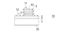
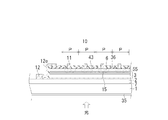
- FIG. 1A and 1B are diagrams showing a light receiving element 10 according to Embodiment 1 of the present invention.
- FIG. 1A shows a light receiving element in which pixels are two-dimensionally arranged
- FIG. 1B shows a single pixel light receiving element. It is. Both are the light receiving elements of the present invention, but the description of the light receiving element having the two-dimensionally arranged pixels includes the description of the single pixel light receiving element. The element will be described.
- the light receiving element 10 has the following group III-V semiconductor stacked structure.
- the type 2 (InAs / GaSb) MQW is the light-receiving layer 3. It has a cut-off wavelength of 3 ⁇ m or more, and has light receiving sensitivity to light in the near infrared to mid infrared (for example, wavelength 3 ⁇ m to 12 ⁇ m).
- This MQW is preferably formed, for example, as a single (InAs / GaSb) pair, about 100 to 300 pairs.
- the thickness of InAs and GaSb can be in the range of 1.5 nm to 7 nm, for example, (InAs thickness 3.6 nm / GaSb thickness 2.1 nm).
- a p-type impurity such as Be.
- InAs is preferably doped with an n-type impurity such as Si so that several tens of pairs of the MQWs on the contact layer 5 side of the entire MQW are formed as an n-type layer.
- Both intermediate layers are not doped with impurities to be i (intrinsic) type.
- a pin photodiode By forming the conductive type region in the MQW, a pin photodiode can be obtained. The independence of each pixel P is ensured by the groove of the mesa structure. A pn junction or a pin junction is formed in the MQW 3 by the impurity doping or undoping described above.
- the electrode 11 of the pixel P is preferably formed of an AuGeNi alloy or the like so as to make ohmic contact with the n-type contact layer 5.
- the ground electrode 12 is preferably formed of a Ti / Pt / Au alloy or the like so as to make ohmic contact with the p-type GaSb buffer layer 2. At this time, the buffer layer preferably has a carrier concentration of 1E18 cm ⁇ 3 or more.
- An AR (Anti-reflection) film 35 covers the back surface of the InP substrate 1 in order to prevent reflection of incident light. AR on the back side of the InP substrate 1
- the structure in which the film 35 is disposed may be referred to as a structure for entering from the substrate side. Further, since the two-dimensional array of pixels P itself is a micro-bump connection method used for connection with a readout circuit, substrate side incidence is inevitable, and it can be said that the structure is incident from the above substrate side.
- / a 1 0.038 (3.8%).
- the GaSb buffer layer 2 has a relatively good crystallinity and is epitaxially grown on the InGaAs intermediate layer 7. The reason for this is not clear at this time. Based on the past research results, it is considered that such good crystallinity is related to the thickness of the GaSb buffer layer and the specificity of the Sb element such as the surfactant effect. It is done. In general, the greater the degree of lattice mismatch, the more misfit dislocations increase unless the film thickness of the layer to be grown is reduced, and an epitaxial film with good crystallinity cannot be obtained.
- the critical film thickness is determined by the Matthews and Blakeslee equation (for example, A. Braun et.al. Journal of Crystal Growth 241 (2002) 231-234) according to the mechanical equilibrium theory or the People and Bean equation according to the energy equilibrium theory. Desired.
- a diagram showing the relationship between the critical film thickness and the degree of lattice mismatch based on these equations is shown in “Masayoshi Umeno, Tetsuo Soga: Crystal Growth Handbook (Kematsu Keisho, Kyoritsu Shuppan, 1995) p. 699”. Has been.
- InP / GaSb has a lattice mismatch of 0.038 as described above. According to the above-mentioned crystal growth handbook, in this case, it is about 4 nm (0.004 ⁇ m) according to the People and Bean equation and about 1 nm (0.001 ⁇ m) according to the Matthews and Blakeslee equation.
- the thickness of the GaSb buffer layer 2 is preferably 0.2 ⁇ m or more. Therefore, in the present embodiment, the thickness of the GaSb buffer layer 2 is several tens of times the critical film thickness. Even based on approximately 4 nm according to the People and Bean equation for calculating the critical film thickness, the thickness is 50 times or more. The thickness may be 100 times or more.
- the reason why the InGaAs intermediate layer 7 is disposed is as follows. That is, the InP substrate 1 has good crystallinity and excellent surface flatness. However, when heat treatment is performed in the film formation chamber in order to remove the oxide film or the like, the surface oxide film is removed and the flatness of the surface deteriorates to increase the roughness. It has been confirmed that a GaSb buffer layer can be directly epitaxially grown thereon. However, the surface of the InGaAs intermediate layer 7 with good flatness can be obtained by epitaxially growing the InGaAs intermediate layer 7 on the InP substrate 1 subjected to the heat treatment for removing the oxide film.
- the surface roughness of the GaSb buffer layer 2 can be reduced and a GaSb buffer layer with good flatness can be obtained.
- a type 2 (InAs / GaSb) MQW is grown on the GaSb buffer layer 2 as a light-receiving layer, a multi-quantum well structure with good flatness can be obtained.
- several hundreds of single layers having a thickness of about 1.5 nm to 5 nm are stacked. Therefore, the flatness of the surface is very important in obtaining a multi-quantum well structure with good crystallinity. Flatness becomes more important as the thickness of a single layer in a multiple quantum well structure is thinner.
- the intended multiple quantum well structure cannot be formed unless the flatness is good.
- Standards for measuring flatness include Rms roughness, surface unevenness profile by an atomic force microscope, and the like. Regardless of the standard, a correlation with the crystallinity is recognized, but the numerical quantification is lacking, but the surface unevenness profile has a good correlation with the crystallinity or dark current.
- the GaSb buffer layer 2 grown on the InGaAs intermediate layer 7 exhibits a mirror surface and is flat without unevenness.
- the XRD main diffraction peak FWHM (full width at half maximum) of the GaSb buffer layer 2 is preferably 300 seconds or less.
- the carrier concentration in the p-type GaSb buffer layer 2 is set to 1E18 cm ⁇ 3 or more in order to reliably realize the ohmic contact.
- the InP substrate 1 has a band gap energy of 1.35 eV. This band gap corresponds to a wavelength of less than 1 ⁇ m. For this reason, the light receiving layer 3 does not absorb the light to be received.
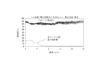
- FIG. 2 is a diagram showing the results of measuring the transmittance (room temperature) of an InP substrate having a thickness of 350 ⁇ m with a Fourier transform infrared spectrophotometer (FT-IR).
- FT-IR Fourier transform infrared spectrophotometer
- the Fe-doped (high resistance) InP substrate is transparent in the wavelength range of 2 ⁇ m to 12 ⁇ m and has no absorption band.
- the transmittance of the sulfur-doped InP substrate also shows the transmittance of the sulfur-doped InP substrate, but the transmittance is almost zero at a wavelength of 5 ⁇ m or more.
- the low transmittance at a wavelength of less than 5 ⁇ m is due to the effect of rough back polishing. Since the transmittance is zero at a wavelength of 5 ⁇ m or more, the sulfur-containing InP substrate cannot be used as a substrate of an infrared light receiving element targeted by the present invention.
- a Type 2 MQW having a cutoff wavelength of 3 ⁇ m or more it is common to use a III-V group compound semiconductor having a lattice constant larger than that of InP as the material constituting the MQW layer.
- a cut-off wavelength of 3 ⁇ m or more cannot be realized even if the transition energy difference of electrons during light reception is reduced by using Type 2 MQW. Since the InGaAs intermediate layer 7 in FIGS. 1A and 1B is lattice matched to the InP substrate, the band gap is not so small as to absorb the light received by the type 2 MQW. It can be considered that the InGaAs intermediate layer 7 is equivalent to the InP substrate 1 for light in the near-infrared to mid-infrared region. When realizing a cutoff wavelength of 3 ⁇ m or more with a type 2 MQW, for example, a GaSb substrate is usually used.
- a group III-V compound semiconductor having a large lattice constant such as GaSb often has an absorption band in the near-infrared to mid-infrared wavelength region.
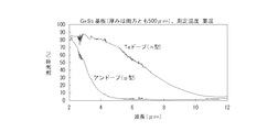
- GaSb has absorption by free carriers in the mid-infrared region as shown in FIG.
- FIG. 3 is a graph showing the results of measuring the transmittance (room temperature) of a GaSb substrate having a thickness of 500 ⁇ m by FT-IR. According to FIG. 3, the undoped GaSb substrate has a transmittance of almost zero at a wavelength of 5 ⁇ m or more.
- the Te-doped GaSb substrate which has a slightly higher transmittance than the undoped GaSb substrate, gradually decreases in transmittance from about 70% near the wavelength of 5 ⁇ m to about 50% near the wavelength of 6.5 ⁇ m, and the wavelength of 8 ⁇ m. It has fallen to 25% or less by the above. It is difficult to use a GaSb substrate exhibiting such a transmittance as a light-receiving element for the infrared region. For example, after manufacturing an epitaxial wafer, it is necessary to delete the GaSb substrate or greatly reduce the thickness, which leads to an increase in man-hours and a deterioration in quality.
- the GaSb buffer layer 2 having good crystallinity can be grown on the InP substrate 1 / InGaAs intermediate layer 7 having no absorption band in the near-infrared to the mid-infrared, and a cut is formed on the GaSb buffer layer 2 Type 2 (InAs / GaSb) MQW having an off wavelength of 3 ⁇ m or more is formed as a light-receiving layer.
- the InGaAs intermediate layer 7 and the thick InP substrate 1 do not absorb the target light.
- the sensitivity to the light to be received can be improved.
- an InP substrate having good crystallinity can be obtained stably.
- the light-receiving layer made of (InAs / GaSb) MQW having good crystallinity. 3 can be obtained at any part and at any opportunity. As a result, elements with uniform characteristics can be manufactured with high yield. Furthermore, since the InP substrate can be obtained with a larger diameter than the GaSb substrate, it is excellent in mass productivity. Furthermore, since the InP substrate is less expensive than the GaSb substrate, the light receiving element 10 and thus the detection device 50 that are excellent in economic efficiency can be provided.
- FIG. 4 is a diagram showing a hybrid detection apparatus in which the light receiving element 10 of FIG. 1 and a readout circuit 70 formed on silicon (Si) are connected.
- the read circuit 70 is a CMOS (Complimentary Metal Oxide Semiconductor).
- the pixel electrode 11 that is conductively connected to the n-type contact layer 5 is conductively connected to the readout electrode 71 with the bumps 9 and 79 interposed therebetween.
- the ground electrode 12 conductively connected to the p-type buffer layer 2 has the wiring electrode 12e transmitted along the protective film 43 so as to be aligned with the height of the pixel electrode 11, and a CMOS ground electrode 72 and bumps interposed therebetween. Conductive connection. According to the connection of the micro bump connection system with the bumps interposed as described above, a compact and downsized detection device can be obtained even if the pixel pitch is reduced and the pixels are high density.
- FIG. 5 is a plan view showing the semiconductor epitaxial wafer 1a in a process in the middle of manufacturing the light receiving element 10 of FIG.
- the GaSb buffer layer 2 is grown on the InP substrate 1 / InGaAs intermediate layer.
- the GaSb buffer layer 2 has a thickness of 1 ⁇ m or more, has a mirror surface, and is flat without unevenness.
- the FWHM of the main peak by XRD is 300 seconds or less.
- / a 1 about 0.038 (3.8%).
- Such good crystallinity is considered to be derived from the fact that the GaSb buffer layer is thick and is a layer containing Sb.
- FIG. 5 is a diagram of the stage where the GaSb buffer layer 2 is formed.
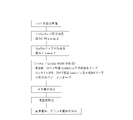
- FIG. 6 is a flowchart showing a method for manufacturing the light receiving element 10 of FIG.
- an InP substrate is prepared, and the oxide film is removed by heating while irradiating a molecular beam of arsenic (As), and then an InGaAs intermediate layer 7 is epitaxially grown.
- the composition of the InGaAs intermediate layer 7 is adjusted so that its lattice constant is the same as that of the InP substrate.
- the InGaAs intermediate layer 7 is epitaxially grown to a thickness of 0.05 ⁇ m or more, for example, about 0.15 ⁇ m.
- a GaSb buffer layer 2 is grown on the InGaAs intermediate layer 7 to a thickness of 1 ⁇ m or more.
- the growth method is not particularly limited, and MBE (Molecular Beam Epitaxy) method, MOVPE (Metal Organic Vapor Phase Epitaxy) method and the like can be used.
- MBE Molecular Beam Epitaxy
- MOVPE Metal Organic Vapor Phase Epitaxy
- the MQW is preferably about 150 pairs or more as a whole.
- p-type impurity Be is doped into about 50 MQW GaSb near the InP substrate 1 during MQW growth.
- the MQW formed thereafter is an intrinsic semiconductor (i-type: intrinsic) as undoped.
- n-type impurity Si is doped into the final InAs of about 50 MQW pairs.
- the pin junction is also a kind of pn junction.
- a mesa structure in which a trench is inserted between the pixels P is formed by etching. Etching is performed by wet etching with phosphoric acid + hydrogen peroxide water + water, or dry etching with hydrogen iodide or silicon chloride gas. As a result, each pixel P can prevent crosstalk and the like independently of surrounding pixels.
- the surface is covered with a protective film (passivation film) 43 that protects the surface of the mesa structure.
- the protective film (passivation film) 43 an SiO 2 film or the like is preferably used.
- the pixel electrode 11 and the ground electrode 12 are formed by photolithography.
- the light receiving element 10 includes the light receiving layer 3 of type 2 (InAs / GaSb) MQW having a cutoff wavelength of 3 ⁇ m or more on the GaSb buffer layer 2 on the InP substrate 1, so that even in the case of substrate back-side incidence, Since the InP substrate 1 having a large thickness does not absorb light of the target wavelength, the light receiving sensitivity can be increased.
- the InP substrate and InGaAs intermediate layer 7 having excellent crystallinity as the base of the GaSb buffer layer 2, the reliable reason is unknown, but the GaSb buffer layer 2 having excellent crystallinity can be obtained. .
- the light receiving layer 3 of type 2 (InAs / GaSb) MQW having a low lattice defect density can be obtained, and the dark current of the light receiving element can be reduced. Furthermore, since the InP substrate 1 is less expensive than the GaSb substrate, it is possible to provide a light receiving element and a detection device that are excellent in economy.
- FIG. 7 is a cross-sectional view showing the light receiving element 10 according to the second embodiment of the present invention.
- the pixel P includes an n-type region 6 selectively diffused from the opening of the SiN selective diffusion mask pattern 36 and a pn junction 15 positioned at the tip of the n-type region 6 as main parts.
- the pn junction 15 reaches the light receiving layer 3. Further, as described above, a pi junction may be used.
- Each pixel P is separated from surrounding pixels by a region that is not selectively diffused.
- the structure of the III-V compound semiconductor stack is as follows: ⁇ InP substrate 1 / InGaAs intermediate layer 7 / p-type GaSb buffer layer 2 / type 2 (InAs / GaSb) MQW light-receiving layer 3 / p-type contact layer 55> .
- the region in contact with the pixel electrode 11 is the n-type region 6 in which n-type impurities are selectively diffused.
- Each pixel P is separated by a region that is not selectively diffused, and the crystal layer remains as it is. For this reason, since the side walls of the pixels are not exposed unlike the mesa structure, the crystal is hardly damaged. As a result, it is easy to realize a low dark current.
- the description of the first embodiment is applied as it is.
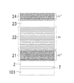
- FIG. 8A is a cross-sectional view showing the epitaxial wafer in the third embodiment of the present invention
- FIG. 8B is a cross-sectional view showing the light receiving element 10 in the third embodiment of the present invention.
- the semiconductor epitaxial wafer in FIG. 8A has the following laminated structure.
- InAs is doped with n-type impurity silicon (Si) and GaSb is not doped.
- the n-type MQW 22 of (InAs / GaSb) positioned on the n + -type MQW 21 is, for example, 100 pairs and has an n-type carrier concentration of 1E16 cm ⁇ 3 .
- the n-type carrier concentration 1E16 cm ⁇ 3 in the n-type MQW 22 is a concentration realized without intentionally introducing n-type impurities.
- AlGaSb, AlAsSb, or the like having a wide band gap and having a conduction band bottom that is higher than the bottom of the upper and lower MQW conduction bands can be used.
- a single layer is usually used, but MQW may be used.
- MQW may be used.
- the contact layer in which the pixel electrode 11 is to be arranged is, for example, 20 pairs, and is an n + type MQW 24 having a carrier concentration of 2e18 cm ⁇ 3 or more.
- InAs is doped with n-type impurity silicon (Si) and GaSb is not doped.
- the pixel P is separated from the peripheral portion by mesa etching only to the contact layer of the n + -type MQW 24 or to a part of the barrier layer.
- the pixel electrode 11 is formed of a Ti / Pt / Au alloy or the like so as to make ohmic contact with the n type contact layer of the n + type MQW 24.
- the ground electrode 12 is preferably made of Ti / Pt / Au alloy or the like so as to make ohmic contact with the n + type MQW 21 positioned in contact with the buffer layer 2.
- both the pixel electrode 11 and the ground electrode 12 are n-side electrodes.
- light reception is detected by capturing holes that diffuse and reach the pixel electrode among the electron-hole pairs generated by light reception. Since the movement of the holes to the pixel electrode is due to diffusion, the mesa structure groove for pixel separation can be shallowed. As a result, the noise current flowing through the side wall of the mesa structure can be kept low.
- the surface is covered with an AR film, a protective film, or the like, as in the first embodiment.
- the pixel electrode 11 and a readout electrode of a readout circuit are conductively connected through a bump.
- the ground electrodes are also conductively connected.
- the advantages of providing the GaSb buffer layer 2 on the InP substrate 1 / InGaAs intermediate layer 7 are the same as those in the first and second embodiments.
- the semiconductor epitaxial wafer 1a shown in FIG. 5 (before the formation of the light receiving layer 3) was produced and verified.
- the method for producing the semiconductor epitaxial wafer of the example of the present invention is as follows. ⁇ Test body>: The InP substrate 1 was loaded into the MBE deposition chamber, and the oxide film was removed by heating while irradiating the As molecular beam. On top of that, an InGaAs intermediate layer 7 having a composition matched to the lattice constant of InP was epitaxially grown to a thickness of 0.15 ⁇ m by MBE, and then a GaSb buffer layer was also grown by MBE. A GaSb buffer layer was grown to a thickness of 2 ⁇ m at a substrate temperature of 400 ° C.
- the growth rate was 1.1 ⁇ m / hour (about 1 ML / second).
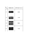
- the surface roughness (root mean roughness (Rms roughness)) measurement and the cross-sectional profile of the semiconductor epitaxial wafer produced by the above method were analyzed. In either case, an atomic force microscope was used and the measurement was performed in accordance with JIS B0601, JIS B0601, and the like. In order to investigate the action of the InGaAs intermediate layer 7, measurement was also performed on the next test piece at an intermediate stage.
- S1 Stage of InP substrate 1 immediately before growing InGaAs intermediate layer 7, that is, after heating for removing the oxide film
- S2 Stage of growing InGaAs intermediate layer 7 on InP substrate 1
- S3 Stage in which the GaSb buffer layer 2 was grown on the InGaAs intermediate layer 7
- R1 Stage in which the GaSb buffer layer 2 was grown directly on the InP substrate 1 as a test specimen for reference
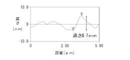
- FIG. 9 is a diagram showing a concavo-convex profile of the surface of the GaSb buffer layer of the test body (S3). That is, the surface flatness of the GaSb buffer layer 7 of InP substrate 1 / InGaAs intermediate layer 7 / GaSb buffer layer 2 is shown.
- FIG. 10 is a diagram showing a surface roughness profile when a GaSb buffer layer is grown directly on the InP substrate 1 in the test sample (R1) of the reference example. Comparing FIG. 9 and FIG. 10, the surface profile in FIG. 9 in which the InGaAs intermediate layer 7 is disposed is clearly smaller in surface irregularities than the surface profile in FIG. 10, and is excellent in flatness.
- FIG. 11A and FIG. 11B are diagrams showing a surface profile in the middle of producing the test body (S3) shown in FIG.
- FIG. 11A is a surface profile of the test body (S1) InP substrate 1 after the heat treatment to remove the oxide film.
- FIG. 11B is a surface profile of the InGaAs intermediate layer 7 epitaxially grown on the InP substrate 1.
- the height (unevenness) scale in FIG. 11A is less sensitive than half the height scale in FIG. 11B.
- the height of the unevenness is almost the same as or slightly higher than the height of the unevenness in FIG. 11B, but the height of the unevenness is larger in FIG. 11A.
- the InGaAs intermediate layer is epitaxially grown on the InP substrate 1
- the unevenness of the InGaAs intermediate layer 7 is leveled, and the flatness is clearly improved. Therefore, it is possible to obtain a GaSb buffer layer with better flatness by growing the GaSb buffer layer on the InP substrate 1 / InGaAs intermediate layer 2 than growing the GaSb buffer layer 2 directly on the InP substrate 1. .
- the crystallinity of the tens to hundreds of multiple quantum well structures formed on the GaSb buffer layer 2 is strongly influenced by the flatness of the underlying layer. As described above, flatness is more important as the thickness of a single layer in a multiple quantum well structure is thinner. By using the InGaAs intermediate layer 7, improved crystallinity can be obtained in the type 2 multiple quantum well structure constituting the light receiving layer, and a low dark current can be realized.
- the root mean square roughness becomes half or less.
- the root mean square roughness of the GaSb buffer layer is smaller when the GaSb buffer layer is grown on the InP substrate 1 / InGaAs intermediate layer 7 than when the GaSb buffer layer is directly grown on the InP substrate 1.
- the mean square roughness seems to be averaged more than the raw unevenness profile in the cross-sectional profile, the difference in the mean square roughness numerical value is alleviated.
- a type 2 MQW light-receiving layer having a large lattice constant is grown in contact with the GaSb buffer layer 2 having good flatness despite the large lattice constant. can do.
- This light receiving layer has a cutoff wavelength of 3 ⁇ m or more, and the InP substrate does not absorb light in the wavelength region.
- a GaSb substrate when used, it has an absorption band due to free carriers in the wavelength range. Since the substrate is thick, this absorption causes a serious reduction in sensitivity.
- the problem of absorption by the substrate can be avoided, and high sensitivity at a wavelength of 3 ⁇ m or more can be maintained.
- the light receiving element or the like of the present invention high light receiving sensitivity can be maintained in the near infrared region to the mid infrared region.
- an InP substrate having stable quality, large diameter, and economy is used for the substrate, a high-quality light receiving element or the like can be provided at low cost.
Landscapes
- Engineering & Computer Science (AREA)
- Chemical & Material Sciences (AREA)
- Nanotechnology (AREA)
- Physics & Mathematics (AREA)
- Life Sciences & Earth Sciences (AREA)
- Biophysics (AREA)
- Optics & Photonics (AREA)
- Crystallography & Structural Chemistry (AREA)
- Light Receiving Elements (AREA)
- Manufacturing & Machinery (AREA)
- Solid State Image Pick-Up Elements (AREA)
Abstract
近赤外域~中赤外域にわたって高い受光感度を持ち、経済性を維持しながら安定して高品質が得られる、受光素子等を提供する。波長3μm~12μmの光に透明なInP基板と、InP基板上にエピタキシャル成長した中間層と、その中間層に接して位置するGaSbバッファ層と、GaSbバッファ層上にエピタキシャル成長したタイプ2の多重量子井戸構造である受光層とを備え、GaSbバッファ層が形式的な格子整合条件の範囲を超えながら、中間層にエピタキシャル成長していることを特徴とする。
Description
本発明は、近赤外域~中赤外域の光を受光対象とする、受光素子、半導体エピタキシャルウエハ、検出装置および受光素子の製造方法に関するものである。
近赤外域~中赤外域の光は、動植物などの生体や環境に関連した吸収スペクトル域に対応するため、これら波長域の光の検出器の開発が行われている。受光素子の受光層にはIII-V族化合物半導体を用いたものが主流となっている。たとえば受光層にExtended-InGaAsを用いることで波長2.6μmまで感度を有する受光素子アレイを組み込んだ検出器の例が発表されている(非特許文献1)。その受光素子アレイでは、窓層にはInGaAs受光層に格子整合するInAsPを用いている。
また、GaSb基板を用いたタイプ2の(InAs/GaSb)の多重量子井戸構造を受光層とする受光素子の提案がなされている(非特許文献2)。この受光素子によれば、波長12μmの近くにまで感度を持つことが示されている。
また、GaSb基板を用いたタイプ2の(InAs/GaSb)の多重量子井戸構造を受光層として、その受光層の中間にバリア層を配置したnBn(n型層/バリア層/n型層)構造の受光素子が提案されている(非特許文献3)。nBn構造の受光素子はpin構造の受光素子と比較して、光の検出に正孔の拡散を用いるため画素分離のためのメサエッチングが浅くて済み、メサ構造の側壁を流れるノイズ電流を小さくできる利点がある。
また、GaSb基板を用いたタイプ2の(InAs/GaSb)の多重量子井戸構造を受光層として、その受光層の中間にバリア層を配置したnBn(n型層/バリア層/n型層)構造の受光素子が提案されている(非特許文献3)。nBn構造の受光素子はpin構造の受光素子と比較して、光の検出に正孔の拡散を用いるため画素分離のためのメサエッチングが浅くて済み、メサ構造の側壁を流れるノイズ電流を小さくできる利点がある。
高橋秀夫ら「近赤外用InGaAs光検出器」,OPTRONICS(1997),No.3, pp.107-113
Binh-Minh Nguyen, Darin Hoffman, Yajun Wei, Pierre-Yves Delaunay,Andrew Hood, and Manijeh Razeghi, "Very high quantum efficiency in type-II InAs/GaSb superlattice photodiode with cutoff of 12 μm" Appl. Phys. Lett., Vol.90, 231108
H.S.Kim, E.Plis, J.B.Rodriguez, G.D.Bishop, Y.D.Sharma, L.R.Dawson,S.Krishna, J.Bundas, R.Cook, D.Burrows, R.Dennis, K.Patnaude, A.Reisinger andM.Sundaram, "Mid-IR focal plane array based on type-II InAs/GaSb strain layersuperlattice detector with nBn design" Appl. Phys.Lett., Vol.92, 183502
しかし、上記の非特許文献1の近赤外用InGaAs光検出器(イメージセンサ)では、InP基板に格子整合しない組成のInGaAsを受光層としているため、暗電流が大きくなりノイズが大きい。また検出可能な波長は、2.6μmを超えることは難しい。
非特許文献2の受光素子については、GaSb基板は高価であり、品質にも大きなばらつきがみられ、量産性という点で問題がある。とくに本質的な問題は、GaSbは中赤外域に自由キャリアによる吸収があるため、アレイ化した画素において必然となる基板裏面入射において感度の低下を生じる。
非特許文献3の受光素子については、上記の非特許文献2と同様の問題があり、量産性という点で、困難に遭遇する。
非特許文献2の受光素子については、GaSb基板は高価であり、品質にも大きなばらつきがみられ、量産性という点で問題がある。とくに本質的な問題は、GaSbは中赤外域に自由キャリアによる吸収があるため、アレイ化した画素において必然となる基板裏面入射において感度の低下を生じる。
非特許文献3の受光素子については、上記の非特許文献2と同様の問題があり、量産性という点で、困難に遭遇する。
本発明は、近赤外域~中赤外域にわたって高い受光感度を持ち、経済性を維持しながら安定して高品質が得られる、受光素子、そこで用いられる半導体エピタキシャルウエハ、検出装置、および受光素子の製造方法を提供することを目的とする。
本発明の受光素子は、III-V族化合物半導体により形成される。この受光素子は、波長3μm~12μmの光に透明なInP基板と、InP基板上にエピタキシャル成長した中間層と、その中間層に接して位置するバッファ層と、バッファ層上にエピタキシャル成長し、カットオフ波長3μm以上のタイプ2の多重量子井戸構造である受光層とを備える。そして、格子定数a2を持つバッファ層、格子定数a1を持つ中間層、および格子定数aoを持つInP基板において、|a1-ao|/ao、の値が形式的な格子整合条件の範囲内にあり、|a2-a1|/a1、および|a2-ao|/ao、の値が形式的な格子整合条件の範囲を超えながら、当該バッファ層が前記中間層上にエピタキシャル成長しており、そのバッファ層が、GaSb層から構成されていることを特徴とする。
III-V族化合物半導体では、元素の組成を変えることにより格子定数が変化するので、エピタキシャル層を成長するとき下層の格子定数に整合するようにエピタキシャル層の組成をきめ細かく変えるのが普通である。これによって、格子欠陥密度の小さいIII-V族化合物半導体の積層体が形成され、受光素子において最重要視される指標の1つである暗電流を低くすることができる。受光素子に限らず他の半導体素子でも格子欠陥密度を低くすることは一定レベルの特性を得るために必要である。このようなIII-V族化合物半導体に特有の、またはIII-V族に限らず化合物半導体に特有の事情を反映して、低い格子欠陥密度を重視することを考える。その場合、一般に、下層の格子定数s1とその上にエピタキシャル成長される上層の格子定数s2で表される格子不整合度:|s1-s2|/(s2またはs1)はできるだけ低い値、たとえば、InGaAs/InP系では(0.002乃至0.003)以下が望ましい。また、一般に、格子整合は上記の格子不整合度が0.005以下ということが知られている。これらを考え合わせて、格子不整合度が0.005以下という範囲を、上述の形式的な格子整合条件の範囲とみることができる。すなわち、形式的な格子整合条件の範囲を超える、とは、格子不整合度が0.005を超えるということである。
しかしながら、実際には、格子不整合度の限界値は、材料系に依存するため、本発明が対象とするGaSb/InP系では、格子不整合度が大きくても結晶性の良好なIII-V族化合物半導体の積層体を形成することができる。これまでの形式的に格子定数のみを取り入れた格子整合条件では、下層に対して上層がエピタキシャル成長するか否かは決めることができない。本発明は、まさにこのような例が現れた実証データに基づく発明である。
ここで、バッファ層が中間層に格子整合している、と述べずに、エピタキシャル成長している、としたのは、格子整合という用語には、成長層および被成長層の両方の格子定数が近い範囲にあることを暗黙に意味する場合もあり、そのような誤解を避けるためにエピタキシャル成長の語を用いた。換言すれば、成長層および被成長層の両方の格子定数が大きく相違するにもかかわらず、低い格子欠陥密度で、“格子整合”または“ほぼ格子整合”を保ちながら成長する場合をエピタキシャル成長と呼ぶ。
上記の構成によれば、良好な結晶性で知られるInP基板を用い、そのInP基板上に中間層をエピタキシャル成長し、その中間層上に、中間層に対してもInP基板に対しても、格子整合条件に適合しないバッファ層をエピタキシャル成長する。そして、目的とする多重量子井戸構造を、そのバッファ層上にエピタキシャル成長することができる。格子定数の見地から、多重量子井戸構造とバッファ層とは、格子整合条件の範囲内にある。
InP基板を使用する意味は次のとおりである。すなわち、InPのバンドギャップは1.35eVなので、カットオフ波長3μmの受光層が受光対象とする波長域の光は吸収しない。バンドギャップ1.35eVは波長1μm弱の短い波長に対応する。このため、基板裏面入射が必然となる二次元配列された画素を備える受光素子において、基板に対象光がまったく吸収されないので、高い受光感度を保持できる。カットオフ波長が3μm以上の多重量子井戸構造には、たとえタイプ2の多重量子井戸構造であっても、InP(格子定数5.869Å)よりも格子定数が大きいIII-V族化合物半導体の基板を用いるのが普通である。タイプ2の多重量子井戸構造を用いて受光における電子の遷移エネルギを小さくしても、カットオフ波長3μmという長い波長(小さい遷移エネルギ)を実現するには、InPよりも格子定数の大きい基板が適していると思われがちである。しかし、InP基板よりも格子定数の大きい基板は、大きな格子定数も含む種々の要因により近赤外~中赤外の光を吸収する。基板は厚みが厚いため、基板による対象光の吸収は、大きな感度低下の要因となる。
しかしながら、実際には、格子不整合度の限界値は、材料系に依存するため、本発明が対象とするGaSb/InP系では、格子不整合度が大きくても結晶性の良好なIII-V族化合物半導体の積層体を形成することができる。これまでの形式的に格子定数のみを取り入れた格子整合条件では、下層に対して上層がエピタキシャル成長するか否かは決めることができない。本発明は、まさにこのような例が現れた実証データに基づく発明である。
ここで、バッファ層が中間層に格子整合している、と述べずに、エピタキシャル成長している、としたのは、格子整合という用語には、成長層および被成長層の両方の格子定数が近い範囲にあることを暗黙に意味する場合もあり、そのような誤解を避けるためにエピタキシャル成長の語を用いた。換言すれば、成長層および被成長層の両方の格子定数が大きく相違するにもかかわらず、低い格子欠陥密度で、“格子整合”または“ほぼ格子整合”を保ちながら成長する場合をエピタキシャル成長と呼ぶ。
上記の構成によれば、良好な結晶性で知られるInP基板を用い、そのInP基板上に中間層をエピタキシャル成長し、その中間層上に、中間層に対してもInP基板に対しても、格子整合条件に適合しないバッファ層をエピタキシャル成長する。そして、目的とする多重量子井戸構造を、そのバッファ層上にエピタキシャル成長することができる。格子定数の見地から、多重量子井戸構造とバッファ層とは、格子整合条件の範囲内にある。
InP基板を使用する意味は次のとおりである。すなわち、InPのバンドギャップは1.35eVなので、カットオフ波長3μmの受光層が受光対象とする波長域の光は吸収しない。バンドギャップ1.35eVは波長1μm弱の短い波長に対応する。このため、基板裏面入射が必然となる二次元配列された画素を備える受光素子において、基板に対象光がまったく吸収されないので、高い受光感度を保持できる。カットオフ波長が3μm以上の多重量子井戸構造には、たとえタイプ2の多重量子井戸構造であっても、InP(格子定数5.869Å)よりも格子定数が大きいIII-V族化合物半導体の基板を用いるのが普通である。タイプ2の多重量子井戸構造を用いて受光における電子の遷移エネルギを小さくしても、カットオフ波長3μmという長い波長(小さい遷移エネルギ)を実現するには、InPよりも格子定数の大きい基板が適していると思われがちである。しかし、InP基板よりも格子定数の大きい基板は、大きな格子定数も含む種々の要因により近赤外~中赤外の光を吸収する。基板は厚みが厚いため、基板による対象光の吸収は、大きな感度低下の要因となる。
上記のようにInP基板/中間層上にGaSb層からなるバッファ層を配置し、カットオフ波長3μm以上の多重量子井戸構造の受光層を配置することによって、近赤外~中赤外において高い感度を持つ受光素子を得ることができる。InP基板とGaSbバッファ層との間に挿入される中間層は、表面を平坦にする材料が選択される。上記のように、InP基板は結晶性が良好であるが、表面の平坦性は、加熱による酸化膜の除去などを行った後は、それほど良好ではなく、平坦性の良好な中間層をエピタキシャル成長させることで、より一層平坦性に優れた表面を得ることができる。その平坦性に優れた中間層上にGaSbバッファ層をエピタキシャル成長させることで、その上のタイプ2の多重量子井戸構造の受光層において良好な結晶性を得ることが可能になる。その結果、一層低い暗電流を実現することができる。
GaSb基板ではなく、InP基板/中間層を用いる利点として、上記のようにInP基板は結晶性が安定して良好なものを得られ、かつ中間層は優れた平坦性を有するので、格子欠陥密度の上層への継承が生じても、大幅な結晶性の劣化もしくは平坦性の劣化は抑制される。このため安定して結晶性の良い、かつ平坦性に優れた多重量子井戸構造の受光層を得ることができ、暗電流を低くすることができる。また上記のInP基板/中間層における、安定した良好な、結晶性および平坦性は、受光素子特性の均一化、および歩留まり向上をもたらす。さらに他のIII-V族化合物半導体の基板に比べて大口径の基板を得ることができるので、量産性にも優れる。
GaSb基板ではなく、InP基板/中間層を用いる利点として、上記のようにInP基板は結晶性が安定して良好なものを得られ、かつ中間層は優れた平坦性を有するので、格子欠陥密度の上層への継承が生じても、大幅な結晶性の劣化もしくは平坦性の劣化は抑制される。このため安定して結晶性の良い、かつ平坦性に優れた多重量子井戸構造の受光層を得ることができ、暗電流を低くすることができる。また上記のInP基板/中間層における、安定した良好な、結晶性および平坦性は、受光素子特性の均一化、および歩留まり向上をもたらす。さらに他のIII-V族化合物半導体の基板に比べて大口径の基板を得ることができるので、量産性にも優れる。
なお、多重量子井戸構造の格子定数は、a層とb層との対の繰り返しでMQWが構成される場合、XRD(Xray Diffraction)パターンの周期性から決定される。バッファ層の格子定数については、InP基板上に成長した所定厚みのバッファ層の厚み全体にわたる平均値であるが、ハンドブック等に記載される材料固有の格子定数とほとんど同じである。
上記のバッファ層は、GaSb層から構成される。または、InP基板/中間層、との関係において結晶特性がGaSb層と同じである層(以下、GaSb同等層)、から構成されてもよい。ここで、InP基板/中間層との関係において結晶特性がGaSb層(以下、GaSb同等層)と同じである、とは、Sbを含み、格子定数がGaSb層とほぼ同じであり、InP基板/中間層とは格子整合条件を逸脱しているが、上述の意味でエピタキシャル成長していることをいう。そして、当該GaSb同等層に格子整合して受光層を形成できることをいう。
基板はInP(格子定数a1=5.869Å)、また、中間層はInPと格子整合条件の範囲内にあるIII-V族化合物半導体として、これらInP基板/中間層、よりも格子定数が非常に大きいGaSb(格子定数a2=6.095Å)層、または、GaSb同等層、を介在させて、長波長側に受光感度を持つ、受光層をエピタキシャル成長することができる。バッファ層の厚みは、とくに限定しないが、厚み0.2μm以上とするのがよい。バッファ層の厚みが0.2μm以上ないと、つぎの問題を生じる。すなわち、バッファ層にグランド電極を設けるとき、エピタキシャル層を上層からバッファ層の所定厚みまでエッチングする際、バッファ層内でエッチング停止をする必要がある。バッファ層の厚みが0.2μm以上ないとエッチング停止のばらつき範囲に収まらなくなる。また、厚いほうは、所定範囲内で厚いほうが表層の結晶性を良好にできるので、1μm以上、好ましくは1.5μm以上または2μm以上とするのがよい。
実施の形態において詳しく説明するが、上記のバッファ層の厚み0.2μm以上は、上記中間層(InPと同等の格子定数とみて)/GaSbバッファ層における臨界膜厚との関係でいえば、臨界膜厚をはるかに大きく超えている。格子不整合度が0.038のとき、臨界膜厚は厚く見積もって4nm(0.004μm)程度である。したがって、バッファ層の膜厚は臨界膜厚の数十倍以上ということができる。GaSbバッファ層は、少なくとも臨界膜厚の50倍以上の厚みを有する。100倍以上であってもよい。これはSb元素がもつサーファクタント効果などの特異性も関係していると考えられる。
上記のInP基板/中間層/GaSb層またはGaSb同等層のバッファ層は、格子整合の立場からはGaSb基板の代わりをしているとみることができる。GaSb基板を用いた場合、しかしながら、GaSbは、中赤外域に自由キャリアによる吸収が存在するので、この受光層の対象光を吸収する。基板は厚みが厚いため、GaSb基板による対象光の吸収は大きな感度低下を生じる。InP基板は、上述のように波長3μm以上の光を吸収しないので、良好な感度を保持することができる。
また、InP基板はGaSb基板に比べて、安定して結晶性が良好であり、受光素子の特性の均一化および歩留まり向上を得ることができる。また、InP基板はGaSb基板に比べて大口径が可能であり、量産性の点でも優れている。さらに非常に安価なので、経済性に優れた高品質の受光素子を提供することができる。
基板はInP(格子定数a1=5.869Å)、また、中間層はInPと格子整合条件の範囲内にあるIII-V族化合物半導体として、これらInP基板/中間層、よりも格子定数が非常に大きいGaSb(格子定数a2=6.095Å)層、または、GaSb同等層、を介在させて、長波長側に受光感度を持つ、受光層をエピタキシャル成長することができる。バッファ層の厚みは、とくに限定しないが、厚み0.2μm以上とするのがよい。バッファ層の厚みが0.2μm以上ないと、つぎの問題を生じる。すなわち、バッファ層にグランド電極を設けるとき、エピタキシャル層を上層からバッファ層の所定厚みまでエッチングする際、バッファ層内でエッチング停止をする必要がある。バッファ層の厚みが0.2μm以上ないとエッチング停止のばらつき範囲に収まらなくなる。また、厚いほうは、所定範囲内で厚いほうが表層の結晶性を良好にできるので、1μm以上、好ましくは1.5μm以上または2μm以上とするのがよい。
実施の形態において詳しく説明するが、上記のバッファ層の厚み0.2μm以上は、上記中間層(InPと同等の格子定数とみて)/GaSbバッファ層における臨界膜厚との関係でいえば、臨界膜厚をはるかに大きく超えている。格子不整合度が0.038のとき、臨界膜厚は厚く見積もって4nm(0.004μm)程度である。したがって、バッファ層の膜厚は臨界膜厚の数十倍以上ということができる。GaSbバッファ層は、少なくとも臨界膜厚の50倍以上の厚みを有する。100倍以上であってもよい。これはSb元素がもつサーファクタント効果などの特異性も関係していると考えられる。
上記のInP基板/中間層/GaSb層またはGaSb同等層のバッファ層は、格子整合の立場からはGaSb基板の代わりをしているとみることができる。GaSb基板を用いた場合、しかしながら、GaSbは、中赤外域に自由キャリアによる吸収が存在するので、この受光層の対象光を吸収する。基板は厚みが厚いため、GaSb基板による対象光の吸収は大きな感度低下を生じる。InP基板は、上述のように波長3μm以上の光を吸収しないので、良好な感度を保持することができる。
また、InP基板はGaSb基板に比べて、安定して結晶性が良好であり、受光素子の特性の均一化および歩留まり向上を得ることができる。また、InP基板はGaSb基板に比べて大口径が可能であり、量産性の点でも優れている。さらに非常に安価なので、経済性に優れた高品質の受光素子を提供することができる。
上述のように、中間層を設けることによって、中間層自体の良好な平坦性によって、その上に積層されるエピタキシャル層の平坦性を改善することができる。たとえば、中間層自身の表面のRmsラフネスは、InP基板の表面のRmsラフネスの3/5以下とすることができる。また、表面の平坦性が良好ではなく平坦性の改善が望まれるGaSbバッファ層については、この中間層に接して積層されることで、平坦性が改善される。その場合においても両者を相対値で比較すると、たとえば、中間層の表面のRmsラフネスは、GaSbバッファ層の表面のRmsラフネスに比べて、1/5以下程度になる。
InP基板にエピタキシャル成長する場合、熱処理を行って酸化層を除去するのが通例である。このとき、InP基板の表面はフレッシュになるが平坦性は少し劣化する。中間層の材料は、平坦性の優れたIII-V族化合物半導体を選択する。この中間層の表面は平坦性に優れるため、この上にエピタキシャル成長したGaSbバッファ層についても良好な平坦性を得ることができる。この良好な平坦性は、タイプ2の多重量子井戸構造の受光層に引き継がれて、平坦性に優れた多重量子井戸構造の受光層を得ることができ、低減された暗電流を実現することができる。
InP基板にエピタキシャル成長する場合、熱処理を行って酸化層を除去するのが通例である。このとき、InP基板の表面はフレッシュになるが平坦性は少し劣化する。中間層の材料は、平坦性の優れたIII-V族化合物半導体を選択する。この中間層の表面は平坦性に優れるため、この上にエピタキシャル成長したGaSbバッファ層についても良好な平坦性を得ることができる。この良好な平坦性は、タイプ2の多重量子井戸構造の受光層に引き継がれて、平坦性に優れた多重量子井戸構造の受光層を得ることができ、低減された暗電流を実現することができる。
中間層は、InGaAs層またはGaAsSb層とするのがよい。
技術蓄積がある既存の方法を用いて、平坦性に優れた中間層を形成することができる。
この良好な平坦性は、GaSbバッファ層およびタイプ2の多重量子井戸構造の受光層へと引き継がれる。InGaAs中間層またはGaAsSb中間層の格子定数は、組成を調整してInPと同じに揃えることができる。
技術蓄積がある既存の方法を用いて、平坦性に優れた中間層を形成することができる。
この良好な平坦性は、GaSbバッファ層およびタイプ2の多重量子井戸構造の受光層へと引き継がれる。InGaAs中間層またはGaAsSb中間層の格子定数は、組成を調整してInPと同じに揃えることができる。
中間層の厚みを50nm以上とするのがよい。
中間層の厚みを50nm以上とすることで、InP基板の酸化膜等を加熱によって除去するときに劣化した表面の平坦性を確実に修復して、中間層自身の平坦性を発揮することができる。
中間層の厚みを50nm以上とすることで、InP基板の酸化膜等を加熱によって除去するときに劣化した表面の平坦性を確実に修復して、中間層自身の平坦性を発揮することができる。
波長3μm~12μmの光に透明なInP基板を、硫黄(S)を添加していないInP基板とするのがよい。
硫黄(S)を含むInP基板は、波長3μm以上から透過率が減少して波長5μmで透過率がほとんどゼロに近づき、波長5μm以上でゼロになる。このため、InP基板には硫黄を含有しないものを用いなければならない。
硫黄(S)を含むInP基板は、波長3μm以上から透過率が減少して波長5μmで透過率がほとんどゼロに近づき、波長5μm以上でゼロになる。このため、InP基板には硫黄を含有しないものを用いなければならない。
波長3μm~12μmの光に透明なInP基板としては、とくに、Fe含有InP基板またはノンドープInP基板とするのがよい。
Fe含有InP基板またはノンドープInP基板を用いることで、InP基板は波長3μm~12μmの光に透明になり、この波長域の光を受光対象にする本発明の受光素子の感度を高めることができる。
Fe含有InP基板またはノンドープInP基板を用いることで、InP基板は波長3μm~12μmの光に透明になり、この波長域の光を受光対象にする本発明の受光素子の感度を高めることができる。
受光層内にpn接合を有するようにできる。
上記の構成によって、高い受光感度を持つpin構造の赤外域の受光素子を提供することができる。
上記の構成によって、高い受光感度を持つpin構造の赤外域の受光素子を提供することができる。
または、受光層に、その受光層に格子整合しているIII-V族化合物半導体からなる挿入層を有し、該挿入層の伝導帯の底を、該受光層の伝導帯の底より高いものとすることができる。
これによって、高い受光感度を持つnBn(n型層/バリア層/n型層)構造の赤外域の受光素子を提供することができる。また、画素の独立性を確保しながらリーク電流を小さくすることができる。
これによって、高い受光感度を持つnBn(n型層/バリア層/n型層)構造の赤外域の受光素子を提供することができる。また、画素の独立性を確保しながらリーク電流を小さくすることができる。
受光素子の受光層における多重量子井戸構造を、タイプ2の多重量子井戸構造である{(InAs/GaSb)、(InAs/InGaSb)、(InAsSb/GaSb)および(InAsSb/InGaSb)}のいずれかとすることができる。
これによって、受光素子は、近赤外~中赤外(波長3μm~12μm)に感度をもつ受光層を得ることができる。なお、InAsの格子定数6.058Å、GaSbの格子定数6.095Å、In0.2Ga0.8Sbの格子定数6.172Å、InAs0.92Sb0.08の格子定数6.092Åである。
これによって、受光素子は、近赤外~中赤外(波長3μm~12μm)に感度をもつ受光層を得ることができる。なお、InAsの格子定数6.058Å、GaSbの格子定数6.095Å、In0.2Ga0.8Sbの格子定数6.172Å、InAs0.92Sb0.08の格子定数6.092Åである。
InP基板の裏面から光が入射される構造を有することができる。
InP基板の裏面を入射面とすることで、二次元配列された受光素子(画素)をマイクロバンプ接続方式で読み出し回路(ROIC)の読み出し電極とコンパクトな構造で接続して小型化されたハイブリッド検出装置を得ることができる。というよりは、マイクロバンプ接続方式によらなければ、小型で使いやすいハイブリッド検出装置を得ることができない。その上で、InP基板が近赤外~中赤外の光を吸収しないので、当該波長域に高い感度をもつ受光素子を得ることができる。
ここで、基板の側から光が入射される構造とは、基板裏面に設けた反射防止膜(AR(Anti-reflection)膜などが該当する。また、二次元配列された画素(受光素子)自体も基板裏面入射を予定しているので、当該構造に該当する。
InP基板の裏面を入射面とすることで、二次元配列された受光素子(画素)をマイクロバンプ接続方式で読み出し回路(ROIC)の読み出し電極とコンパクトな構造で接続して小型化されたハイブリッド検出装置を得ることができる。というよりは、マイクロバンプ接続方式によらなければ、小型で使いやすいハイブリッド検出装置を得ることができない。その上で、InP基板が近赤外~中赤外の光を吸収しないので、当該波長域に高い感度をもつ受光素子を得ることができる。
ここで、基板の側から光が入射される構造とは、基板裏面に設けた反射防止膜(AR(Anti-reflection)膜などが該当する。また、二次元配列された画素(受光素子)自体も基板裏面入射を予定しているので、当該構造に該当する。
本発明の検出装置は、上記のいずれかの受光素子と、読み出し回路(ROIC:Read Out IC)とを備え、受光素子における画素電極と、読み出し回路における読み出し電極とがバンプを介在させて接続されていることを特徴とする。
これによって、近赤外~中赤外に高い受光感度をもち、コンパクトで小型化された検出装置を得ることができる。
これによって、近赤外~中赤外に高い受光感度をもち、コンパクトで小型化された検出装置を得ることができる。
本発明の半導体エピタキシャルウエハは、III-V族化合物半導体により形成されている。この半導体エピタキシャルウエハは、波長3μm~12μmの光に透明なInP基板と、InP基板上にエピタキシャル成長した中間層と、中間層に接して位置するGaSbバッファ層と、GaSbバッファ層上にエピタキシャル成長した、タイプ2の多重量子井戸構造の受光層とを備える。そして、格子定数a2を持つバッファ層、格子定数a1を持つ中間層および格子定数aoを持つInP基板において、|a1-ao|/ao、の値が形式的な格子整合条件の範囲内にあり、|a2-a1|/a1、および|a2-ao|/ao、の値が形式的な格子整合条件の範囲を超えながら、当該GaSbバッファ層が中間層上にエピタキシャル成長していることを特徴とする。
III-V族化合物半導体におけるエピタキシャル成長、および形式的な格子整合条件などについては、上記受光素子での説明がそのまま当てはまる。また、バッファ層をGaSb層で構成することの技術的意味についても、上述のとおりである。そして、GaSb同等層で形成することの技術的意味についても、上述のとおりである。
上記の構成によって、良好な結晶性で知られるInP基板、および中間層を用いて、InPと格子整合しないとされる格子定数をもつバッファ層をGaSb層などで形成することでそのバッファ層の結晶性を比較的良好なものとできる。この半導体エピタキシャルウエハ上に当該バッファ層に格子整合するエピタキシャル層を成長させることができる。いわば、InP基板/中間層を用いながら、InPと格子定数が異なる基板を実現することができる。
上記の構成によって、良好な結晶性で知られるInP基板、および中間層を用いて、InPと格子整合しないとされる格子定数をもつバッファ層をGaSb層などで形成することでそのバッファ層の結晶性を比較的良好なものとできる。この半導体エピタキシャルウエハ上に当該バッファ層に格子整合するエピタキシャル層を成長させることができる。いわば、InP基板/中間層を用いながら、InPと格子定数が異なる基板を実現することができる。
上記の半導体エピタキシャルウエハにおいて、中間層は、InGaAs層またはGaAsSb層とするのがよい。
平坦性に優れた中間層を形成することで、GaSbバッファ層およびタイプ2の多重量子井戸構造の平坦性を良好にすることができる。
平坦性に優れた中間層を形成することで、GaSbバッファ層およびタイプ2の多重量子井戸構造の平坦性を良好にすることができる。
上記のエピタキシャルウエハにおいて、波長3μm~12μmの光に透明なInP基板を、Fe含有InP基板またはノンドープInP基板とすることができる。
これによって、厚みが大きい基板が、波長3μm~12μmの範囲の光を吸収しないので、この波長域を受光対象とする本発明に係る受光素子の感度を高めることができる。
これによって、厚みが大きい基板が、波長3μm~12μmの範囲の光を吸収しないので、この波長域を受光対象とする本発明に係る受光素子の感度を高めることができる。
上記の半導体エピタキシャルウエハにおいて、多重量子井戸構造を、タイプ2の多重量子井戸構造である{(InAs/GaSb)、(InAs/InGaSb)、(InAsSb/GaSb)および(InAsSb/InGaSb)}のいずれかとすることができる。
これによって、近赤外~中赤外(波長3μm~12μm)に高い感度をもつ受光素子を作製するための半導体エピタキシャルウエハを提供することができる。
これによって、近赤外~中赤外(波長3μm~12μm)に高い感度をもつ受光素子を作製するための半導体エピタキシャルウエハを提供することができる。
本発明の受光素子の製造方法は、III-V族化合物半導体が積層された受光素子を製造する方法である。この製造方法は、波長3μm~12μmの光に透明なInP基板を準備する工程と、InP基板上に中間層をエピタキシャル成長する工程と、中間層上にGaSbバッファ層をエピタキシャル成長する工程と、GaSbバッファ層上に、カットオフ波長3μm以上のタイプ2の多重量子井戸構造を含む受光層を形成する工程とを備え、多重量子井戸構造を、タイプ2の多重量子井戸構造である{(InAs/GaSb)、(InAs/InGaSb)、(InAsSb/GaSb)および(InAsSb/InGaSb)}のいずれかとすることを特徴とする。
上記の方法によれば、InP基板/中間層に、常識的には格子整合しないと判断される材料であるGaSb層などを用いることで、多重量子井戸構造をエピタキシャル成長できるほど結晶性の良いバッファ層とすることができる。この結果、上記の理由により波長3μm以上に高い受光感度をもつ受光素子を得ることができる。また、InP基板は安定して結晶性が良好な大口径のもの得ることができ、高品質で経済性に優れた受光素子を提供することができる。なお、バッファ層はGaSb同等層で形成してもよいことは上記のとおりである。
受光素子の製造方法において、中間層として、InGaAs層、またはGaAsSb層を成長させるのがよい。
これによって平坦性に優れた、GaSbバッファ層およびタイプ2の多重量子井戸構造を得ることができる。
これによって平坦性に優れた、GaSbバッファ層およびタイプ2の多重量子井戸構造を得ることができる。
本発明の受光素子等によれば、近赤外域~中赤外域にわたって高い受光感度を持ち、経済性を維持しながら安定して高品質が得られる。とくに基板にInP基板を用いるので、上記の波長域の光に対して吸収がなく、良好な感度を得ることができる。また、大口径のInP基板を用いて高い量産性を得ることができる。
1 InP基板、2 GaSbバッファ層、3 受光層、5 n型コンタクト層、6 n型領域、9 受光素子のバンプ、10 受光素子、11 画素電極、12 グランド電極、12e 配線電極、15 pn接合、21 n+型MQW、22 n型MQW、23 バリア層、24 n+型MQW、35 反射防止膜、36 選択拡散マスクパターン、43 保護膜、50 ハイブリッド検出装置、55 p型コンタクト層、70 読み出し回路、71 読み出し電極、72 グランド電極、73 絶縁膜、79 バンプ、101 FeドープInP(100)基板、P 画素。
(実施の形態1)
図1Aおよび図1Bは、本発明の実施の形態1における受光素子10を示す図であり、図1Aは画素が二次元配列された受光素子、図1Bは単一画素の受光素子、を示す図である。どちらも本発明の受光素子であるが、二次元配列された画素をもつ受光素子の説明は、単一画素の受光素子の説明を包含するので、以下では、二次元配列された画素をもつ受光素子について説明する。
図1Aによれば、受光素子10は次のIII-V族半導体積層構造を備える。
<InP基板1/InGaAs中間層7/p型GaSbバッファ層2/タイプ2の(InAs/GaSb)多重量子井戸構造(MQW)/n型コンタクト層5>
このうち、タイプ2の(InAs/GaSb)MQWが、受光層3である。カットオフ波長3μm以上であり、近赤外~中赤外(たとえば波長3μm~12μm)の光に受光感度をもつ。このMQWは、たとえば単一の(InAs/GaSb)を1ペアとして、100~300ペア程度形成されるのがよい。InAsおよびGaSbの厚みは、1.5nm~7nmの範囲、たとえば(InAs厚み3.6nm/GaSb厚み2.1nm)とすることができる。全体のMQWのうち、InP基板1の側の数十ペアのGaSbにはp型不純物たとえばBeをドープするのがよい。また、全体のMQWのうちコンタクト層5の側の数十ペアをn型層とするためにInAsにSiなどのn型不純物をドープするのがよい。両方の中間の層は、i(intrinsic)型とするために不純物をドープしない。このようなMQWの中の導電型領域の形成によって、pinフォトダイオードを得ることができる。各画素Pの独立性は、メサ構造の溝によって確保される。
pn接合またはpin接合は、上記の不純物ドープまたはアンドープにより、MQW3内に形成される。
画素Pの電極11は、n型コンタクト層5にオーミック接触するようにAuGeNi合金等で形成するのがよい。またグランド電極12は、p型GaSbバッファ層2にオーミック接触するようにTi/Pt/Au合金等で形成するのがよい。この際、バッファ層には1E18cm-3以上のキャリア濃度を有するのが望ましい。
光は、InP基板1の裏面から入射される。入射光の反射を防止するためにAR(Anti-reflection)膜35がInP基板1の裏面を被覆する。このInP基板1の裏面にAR
膜35を配置する構造は、基板側から入射するための構造といってよい。また画素Pの二次元配列自体、読み出し回路との接続に用いられるマイクロバンプ接続方式のため、基板側入射は必然であり、上記の基板側から入射するための構造といってよい。
図1Aおよび図1Bは、本発明の実施の形態1における受光素子10を示す図であり、図1Aは画素が二次元配列された受光素子、図1Bは単一画素の受光素子、を示す図である。どちらも本発明の受光素子であるが、二次元配列された画素をもつ受光素子の説明は、単一画素の受光素子の説明を包含するので、以下では、二次元配列された画素をもつ受光素子について説明する。
図1Aによれば、受光素子10は次のIII-V族半導体積層構造を備える。
<InP基板1/InGaAs中間層7/p型GaSbバッファ層2/タイプ2の(InAs/GaSb)多重量子井戸構造(MQW)/n型コンタクト層5>
このうち、タイプ2の(InAs/GaSb)MQWが、受光層3である。カットオフ波長3μm以上であり、近赤外~中赤外(たとえば波長3μm~12μm)の光に受光感度をもつ。このMQWは、たとえば単一の(InAs/GaSb)を1ペアとして、100~300ペア程度形成されるのがよい。InAsおよびGaSbの厚みは、1.5nm~7nmの範囲、たとえば(InAs厚み3.6nm/GaSb厚み2.1nm)とすることができる。全体のMQWのうち、InP基板1の側の数十ペアのGaSbにはp型不純物たとえばBeをドープするのがよい。また、全体のMQWのうちコンタクト層5の側の数十ペアをn型層とするためにInAsにSiなどのn型不純物をドープするのがよい。両方の中間の層は、i(intrinsic)型とするために不純物をドープしない。このようなMQWの中の導電型領域の形成によって、pinフォトダイオードを得ることができる。各画素Pの独立性は、メサ構造の溝によって確保される。
pn接合またはpin接合は、上記の不純物ドープまたはアンドープにより、MQW3内に形成される。
画素Pの電極11は、n型コンタクト層5にオーミック接触するようにAuGeNi合金等で形成するのがよい。またグランド電極12は、p型GaSbバッファ層2にオーミック接触するようにTi/Pt/Au合金等で形成するのがよい。この際、バッファ層には1E18cm-3以上のキャリア濃度を有するのが望ましい。
光は、InP基板1の裏面から入射される。入射光の反射を防止するためにAR(Anti-reflection)膜35がInP基板1の裏面を被覆する。このInP基板1の裏面にAR
膜35を配置する構造は、基板側から入射するための構造といってよい。また画素Pの二次元配列自体、読み出し回路との接続に用いられるマイクロバンプ接続方式のため、基板側入射は必然であり、上記の基板側から入射するための構造といってよい。
本実施の形態における特徴は、次の点にある。
(1)InP基板1の格子定数ao=5.869Åであり、InGaAs中間層7の格子定数a1は、組成を調整してInP基板の格子定数aoと同じに揃えてある。これに対して、GaSbの格子定数a2=6.095Åと、非常に大きい。InGaAs中間層7とInPとの格子不整合度をとると、|a2-a1|/a1=0.038(3.8%)である。下層と上層の格子定数の相違が、非常に大きいにもかかわらず、GaSbバッファ層2は、比較的良好な結晶性を有して、InGaAs中間層7上にエピタキシャル成長している。この理由は、現時点で、明らかでない。これまでの研究結果等を総合して推測すると、このような良好な結晶性はGaSbバッファ層の厚みが厚いこと、および、Sb元素がもつサーファクタント効果などの特異性も関係している、と考えられる。
一般に、格子不整合度が大きいほど、成長する層の膜厚は薄くしないとミスフィット転位が増大して結晶性のよいエピタキシャル膜は得られない。このため結晶成長の分野では、臨界膜厚という概念を設けて、その臨界膜厚の厚み以上では、結晶性の良好なエピタキシャル膜は得られないという考え方が一般的となっている。その臨界膜厚は、力学的平衡理論によるMatthews and Blakesleeの式(例えば、A.Braun et.al. Journal of Crystal Growth 241(2002)231-234)、またはエネルギー平衡理論によるPeople and Beanの式によって求められる。これらの式に基づいて臨界膜厚と、格子不整合度との関係を示した図が、「梅野正義、蘇我哲夫:結晶成長ハンドブック(小松啓編,共立出版,1995)p.699」に示されている。InP/GaSbにおいては、上記のように格子不整合度0.038である。上記結晶成長ハンドブックの図によれば、この場合、People and Beanの式によれば約4nm(0.004μm)であり、Matthews and Blakesleeの式によれば約1nm(0.001μm)である。
上記したように、GaSbバッファ層2の厚みは0.2μm以上とするのがよい。したがって、本実施の形態では、GaSbバッファ層2の厚みは、臨界膜厚の数十倍以上あることになる。臨界膜厚を厚く算定するPeople and Beanの式による約4nmに基づいても、50倍以上の厚みを有する。100倍以上の厚みでもよい。
(2)InGaAs中間層7を配置したのは、次の理由による。すなわちInP基板1は、良好な結晶性を有し、表面の平坦性も優れている。しかし、酸化膜等を除去するために成膜室に入れて加熱処理を行うと、表面の酸化膜が除去されるとともに、表面の平坦性が劣化して粗度が大きくなる。この上に、直接、GaSbバッファ層をエピタキシャル成長することが可能であることは確認してある。しかし、InGaAs中間層7を、酸化膜を除去の加熱処理をしたInP基板1にエピタキシャル成長することで、平坦性の良好なInGaAs中間層7の表面を得ることができる。このInGaAs中間層7に、GaSbバッファ層2をエピタキシャル成長することで、GaSbバッファ層2の表面の粗度を小さくして、平坦性の良好なGaSbバッファ層を得ることができる。このGaSbバッファ層2上に、受光層としてタイプ2の(InAs/GaSb)MQWを成長すると、やはり良好な平坦性の多重量子井戸構造を得ることができる。上述のように、厚み1.5nm~5nm程度の単一層を数百積層するので、表面の平坦性は、良好な結晶性の多重量子井戸構造を得る上で、非常に重要である。多重量子井戸構造内の単一層の厚みが薄いほど、平坦性は重要となる。上述のように、単一層の厚み1.5nmの場合には、平坦性が良好でなければ、意図したとおりの多重量子井戸構造を形成することができない。
平坦性を測る基準には、Rmsラフネス、原子間力顕微鏡等による表面の凹凸プロファイル等がある。どの基準をとっても、結晶性との相関は認められるが、数値的な定量性には欠けるが、表面の凹凸プロファイルが結晶性、もしくは暗電流と良い相関があることが認められた。
InGaAs中間層7上に成長したGaSbバッファ層2は、鏡面を呈して、凹凸がなく平坦である。GaSbバッファ層2についてのXRDの主回折ピークのFWHM(半値全幅)は、300秒以下とするのがよい。p型GaSbバッファ層2におけるキャリア濃度は上記オーミック接触を確実に実現するために、1E18cm-3以上とする。
(3)InP基板1は、バンドギャップエネルギが1.35eVである。このバンドギャップは波長1μm弱に対応する。このため、受光層3が受光対象とする光を吸収しない。
図2は、厚み350μmのInP基板の透過率(室温)を、フーリエ変換赤外分光光度計(FT-IR)で測定した結果を示す図である。Feドープ(高抵抗)InP基板は波長2μm~12μmの波長域で透明であり、吸収帯がない。なお、図2は、硫黄ドープInP基板の透過率も記載するが、波長5μm以上ではほとんど透過率はゼロである。波長5μm未満において透過率が低いのは裏面粗研磨の影響である。波長5μm以上で透過率がゼロであるため、硫黄含有InP基板は、本発明が対象とする赤外域の受光素子の基板には使用することはできない。
カットオフ波長3μm以上のタイプ2のMQWを形成する場合、MQWの層を構成する材料には、InPよりも格子定数の大きいIII-V族化合物半導体を用いるのが普通である。InPに格子整合するIII-V族化合物半導体を用いたのでは、たとえタイプ2のMQWによって受光の際の電子の遷移エネルギ差を小さくしたとしても、カットオフ波長3μm以上を実現することはできない。図1Aおよび図1BにおけるInGaAs中間層7は、InP基板に格子整合するので、バンドギャップは、タイプ2のMQWが受光する光を吸収するほど小さくない。近赤外~中赤外域の光に対して、InGaAs中間層7は、InP基板1と同等であるとみてよい。
カットオフ波長3μm以上を、タイプ2のMQWで実現する場合、たとえばGaSb基板を用いるのが普通である。GaSbのような格子定数の大きいIII-V族化合物半導体は、近赤外~中赤外の波長域に吸収帯を持つ場合が多い。たとえば、GaSbは、図3に示すように中赤外域に自由キャリアによる吸収を持つ。図3は、厚み500μmのGaSb基板の透過率(室温)をFT-IRで測定した結果を示す図である。図3によれば、アンドープGaSb基板は、波長5μm以上で透過率はほとんどゼロである。また、アンドープGaSb基板よりも少し透過率が高いTeドープGaSb基板についても、透過率は、波長5μm付近の70%程度から徐々に低下し、波長6.5μm付近で50%程度になり、波長8μm以上で25%以下に低下している。このような透過率を示すGaSb基板を赤外域を対象とする受光素子用いることは難しい。たとえば、エピタキシャルウエハを製造したあと、GaSb基板を削除するか、大幅に減厚する必要があり、工数の増大および品質劣化を招く。
しかし、上記によれば、近赤外~中赤外に吸収帯を持たないInP基板1/InGaAs中間層7、に結晶性の良いGaSbバッファ層2を成長でき、そのGaSbバッファ層2上にカットオフ波長3μm以上のタイプ2の(InAs/GaSb)MQWを受光層として形成している。この結果、InGaAs中間層7、および厚みが大きいInP基板1が、対象とする光を吸収することはない。この結果、受光対象の光に対する感度を向上させることができる。
(4)GaSb基板に比べて、良好な結晶性のInP基板を安定して得ることができる。
このため、InP基板1/InGaAs中間層7/GaSbバッファ層2/(InAs/GaSb)MQWからなる受光層3、とエピタキシャル成長しても、良好な結晶性の(InAs/GaSb)MQWからなる受光層3を、どの部分でも、またどの機会にも得ることができる。この結果、特性が均一な素子を、歩留まり良く製造することができる。
さらにInP基板はGaSb基板に比べて、大口径のものを得られるので量産性に優れている。さらに、InP基板はGaSb基板に比べて安価であるので、経済性に優れた受光素子10、ひいては検出装置50を提供することができる。
(1)InP基板1の格子定数ao=5.869Åであり、InGaAs中間層7の格子定数a1は、組成を調整してInP基板の格子定数aoと同じに揃えてある。これに対して、GaSbの格子定数a2=6.095Åと、非常に大きい。InGaAs中間層7とInPとの格子不整合度をとると、|a2-a1|/a1=0.038(3.8%)である。下層と上層の格子定数の相違が、非常に大きいにもかかわらず、GaSbバッファ層2は、比較的良好な結晶性を有して、InGaAs中間層7上にエピタキシャル成長している。この理由は、現時点で、明らかでない。これまでの研究結果等を総合して推測すると、このような良好な結晶性はGaSbバッファ層の厚みが厚いこと、および、Sb元素がもつサーファクタント効果などの特異性も関係している、と考えられる。
一般に、格子不整合度が大きいほど、成長する層の膜厚は薄くしないとミスフィット転位が増大して結晶性のよいエピタキシャル膜は得られない。このため結晶成長の分野では、臨界膜厚という概念を設けて、その臨界膜厚の厚み以上では、結晶性の良好なエピタキシャル膜は得られないという考え方が一般的となっている。その臨界膜厚は、力学的平衡理論によるMatthews and Blakesleeの式(例えば、A.Braun et.al. Journal of Crystal Growth 241(2002)231-234)、またはエネルギー平衡理論によるPeople and Beanの式によって求められる。これらの式に基づいて臨界膜厚と、格子不整合度との関係を示した図が、「梅野正義、蘇我哲夫:結晶成長ハンドブック(小松啓編,共立出版,1995)p.699」に示されている。InP/GaSbにおいては、上記のように格子不整合度0.038である。上記結晶成長ハンドブックの図によれば、この場合、People and Beanの式によれば約4nm(0.004μm)であり、Matthews and Blakesleeの式によれば約1nm(0.001μm)である。
上記したように、GaSbバッファ層2の厚みは0.2μm以上とするのがよい。したがって、本実施の形態では、GaSbバッファ層2の厚みは、臨界膜厚の数十倍以上あることになる。臨界膜厚を厚く算定するPeople and Beanの式による約4nmに基づいても、50倍以上の厚みを有する。100倍以上の厚みでもよい。
(2)InGaAs中間層7を配置したのは、次の理由による。すなわちInP基板1は、良好な結晶性を有し、表面の平坦性も優れている。しかし、酸化膜等を除去するために成膜室に入れて加熱処理を行うと、表面の酸化膜が除去されるとともに、表面の平坦性が劣化して粗度が大きくなる。この上に、直接、GaSbバッファ層をエピタキシャル成長することが可能であることは確認してある。しかし、InGaAs中間層7を、酸化膜を除去の加熱処理をしたInP基板1にエピタキシャル成長することで、平坦性の良好なInGaAs中間層7の表面を得ることができる。このInGaAs中間層7に、GaSbバッファ層2をエピタキシャル成長することで、GaSbバッファ層2の表面の粗度を小さくして、平坦性の良好なGaSbバッファ層を得ることができる。このGaSbバッファ層2上に、受光層としてタイプ2の(InAs/GaSb)MQWを成長すると、やはり良好な平坦性の多重量子井戸構造を得ることができる。上述のように、厚み1.5nm~5nm程度の単一層を数百積層するので、表面の平坦性は、良好な結晶性の多重量子井戸構造を得る上で、非常に重要である。多重量子井戸構造内の単一層の厚みが薄いほど、平坦性は重要となる。上述のように、単一層の厚み1.5nmの場合には、平坦性が良好でなければ、意図したとおりの多重量子井戸構造を形成することができない。
平坦性を測る基準には、Rmsラフネス、原子間力顕微鏡等による表面の凹凸プロファイル等がある。どの基準をとっても、結晶性との相関は認められるが、数値的な定量性には欠けるが、表面の凹凸プロファイルが結晶性、もしくは暗電流と良い相関があることが認められた。
InGaAs中間層7上に成長したGaSbバッファ層2は、鏡面を呈して、凹凸がなく平坦である。GaSbバッファ層2についてのXRDの主回折ピークのFWHM(半値全幅)は、300秒以下とするのがよい。p型GaSbバッファ層2におけるキャリア濃度は上記オーミック接触を確実に実現するために、1E18cm-3以上とする。
(3)InP基板1は、バンドギャップエネルギが1.35eVである。このバンドギャップは波長1μm弱に対応する。このため、受光層3が受光対象とする光を吸収しない。
図2は、厚み350μmのInP基板の透過率(室温)を、フーリエ変換赤外分光光度計(FT-IR)で測定した結果を示す図である。Feドープ(高抵抗)InP基板は波長2μm~12μmの波長域で透明であり、吸収帯がない。なお、図2は、硫黄ドープInP基板の透過率も記載するが、波長5μm以上ではほとんど透過率はゼロである。波長5μm未満において透過率が低いのは裏面粗研磨の影響である。波長5μm以上で透過率がゼロであるため、硫黄含有InP基板は、本発明が対象とする赤外域の受光素子の基板には使用することはできない。
カットオフ波長3μm以上のタイプ2のMQWを形成する場合、MQWの層を構成する材料には、InPよりも格子定数の大きいIII-V族化合物半導体を用いるのが普通である。InPに格子整合するIII-V族化合物半導体を用いたのでは、たとえタイプ2のMQWによって受光の際の電子の遷移エネルギ差を小さくしたとしても、カットオフ波長3μm以上を実現することはできない。図1Aおよび図1BにおけるInGaAs中間層7は、InP基板に格子整合するので、バンドギャップは、タイプ2のMQWが受光する光を吸収するほど小さくない。近赤外~中赤外域の光に対して、InGaAs中間層7は、InP基板1と同等であるとみてよい。
カットオフ波長3μm以上を、タイプ2のMQWで実現する場合、たとえばGaSb基板を用いるのが普通である。GaSbのような格子定数の大きいIII-V族化合物半導体は、近赤外~中赤外の波長域に吸収帯を持つ場合が多い。たとえば、GaSbは、図3に示すように中赤外域に自由キャリアによる吸収を持つ。図3は、厚み500μmのGaSb基板の透過率(室温)をFT-IRで測定した結果を示す図である。図3によれば、アンドープGaSb基板は、波長5μm以上で透過率はほとんどゼロである。また、アンドープGaSb基板よりも少し透過率が高いTeドープGaSb基板についても、透過率は、波長5μm付近の70%程度から徐々に低下し、波長6.5μm付近で50%程度になり、波長8μm以上で25%以下に低下している。このような透過率を示すGaSb基板を赤外域を対象とする受光素子用いることは難しい。たとえば、エピタキシャルウエハを製造したあと、GaSb基板を削除するか、大幅に減厚する必要があり、工数の増大および品質劣化を招く。
しかし、上記によれば、近赤外~中赤外に吸収帯を持たないInP基板1/InGaAs中間層7、に結晶性の良いGaSbバッファ層2を成長でき、そのGaSbバッファ層2上にカットオフ波長3μm以上のタイプ2の(InAs/GaSb)MQWを受光層として形成している。この結果、InGaAs中間層7、および厚みが大きいInP基板1が、対象とする光を吸収することはない。この結果、受光対象の光に対する感度を向上させることができる。
(4)GaSb基板に比べて、良好な結晶性のInP基板を安定して得ることができる。
このため、InP基板1/InGaAs中間層7/GaSbバッファ層2/(InAs/GaSb)MQWからなる受光層3、とエピタキシャル成長しても、良好な結晶性の(InAs/GaSb)MQWからなる受光層3を、どの部分でも、またどの機会にも得ることができる。この結果、特性が均一な素子を、歩留まり良く製造することができる。
さらにInP基板はGaSb基板に比べて、大口径のものを得られるので量産性に優れている。さらに、InP基板はGaSb基板に比べて安価であるので、経済性に優れた受光素子10、ひいては検出装置50を提供することができる。
図4は、図1の受光素子10と、シリコン(Si)に形成された読み出し回路70とを接続したハイブリッド検出装置を示す図である。読み出し回路70はCMOS(Complimentary Metal Oxide Semiconductor)である。n型コンタクト層5に導電接続する画素電極11は、読み出し電極71と、それぞれのバンプ9,79を介在させて導電接続されている。またp型バッファ層2に導電接続するグランド電極12は、配線電極12eを保護膜43に沿って伝わらせて画素電極11の高さに揃えて、CMOSのグランド電極72と、バンプを介在させて導電接続させている。
上記のようなバンプを介在させたマイクロバンプ接続方式の接続によれば、画素ピッチを小さくして高密度の画素としても、コンパクトな小型化した検出装置を得ることができる。
上記のようなバンプを介在させたマイクロバンプ接続方式の接続によれば、画素ピッチを小さくして高密度の画素としても、コンパクトな小型化した検出装置を得ることができる。
図5は、図1の受光素子10を作製する途中の工程における半導体エピタキシャルウエハ1aを示す平面図である。受光素子10の仕様によるが、30μmピッチで約8万個の画素が縦横に配列された、8.5mm×10mmのチップ(受光素子)の場合、2インチ径のInP基板から、約11個、取得することができる。4インチ径のInP基板からは約52個を取得することができる。上記のように、GaSb基板を用いるよりも大口径のInP基板を用いることで高い量産性を得ることができる。
図5に示す半導体エピタキシャルウエハ1aは、InP基板1/InGaAs中間層7上にGaSbバッファ層2が成長された状態である。GaSbバッファ層2は、厚み1μm以上であり、鏡面を呈しており、凹凸がなく平坦である。かつ、XRDによる主ピークのFWHMは300秒以下である。しかしながら、|a2-a1|/a1=約0.038(3.8%)である。このような良好な結晶性は、GaSbバッファ層の厚みが厚いこと、およびSbを含む層であることに由来すると考えられる。
受光素子10は、受光層3、コンタクト層5、メサ構造、電極11,12を形成されて、チップの輪郭が次第に明確になった状態で、半導体エピタキシャルウエハ1aから個片化される。図5は、GaSbバッファ層2を形成した段階の図である。
図5に示す半導体エピタキシャルウエハ1aは、InP基板1/InGaAs中間層7上にGaSbバッファ層2が成長された状態である。GaSbバッファ層2は、厚み1μm以上であり、鏡面を呈しており、凹凸がなく平坦である。かつ、XRDによる主ピークのFWHMは300秒以下である。しかしながら、|a2-a1|/a1=約0.038(3.8%)である。このような良好な結晶性は、GaSbバッファ層の厚みが厚いこと、およびSbを含む層であることに由来すると考えられる。
受光素子10は、受光層3、コンタクト層5、メサ構造、電極11,12を形成されて、チップの輪郭が次第に明確になった状態で、半導体エピタキシャルウエハ1aから個片化される。図5は、GaSbバッファ層2を形成した段階の図である。
図6は、図1の受光素子10の製造方法を示すフローチャートである。まず、InP基板を準備して、砒素(As)の分子線照射をしながら加熱して酸化膜を除去したあと、InGaAs中間層7をエピタキシャル成長する。InGaAs中間層7は、その格子定数がInP基板の格子定数と同じになるように組成調整をする。InGaAs中間層7は、厚み0.05μm以上、たとえば0.15μm程度にエピタキシャル成長する。そのInGaAs中間層7上にGaSbバッファ層2を厚み1μm以上に成長する。成長法は、とくに限定しないが、MBE(Molecular Beam Epitaxy)法、MOVPE(Metal Organic Vapor Phase Epitaxy)法などを用いることができる。GaSbバッファ層2成長後、タイプ2の(InAs/GaSb)MQWの受光層3を成長する。タイプ2の遷移(受光)は、InAsとGaSbとの界面を挟んで行われるので、界面の数が多いほうが長波長側の受光感度を高くする。このため、長波長側の感度を重視する場合、MQWは全体で150ペア程度以上とするのがよい。受光層3すなわち上記のMQW内にpn接合を形成するために、MQW成長中に、InP基板1に近い側のMQW50ペア程度のGaSbにp型不純物Beをドープする。そのあとに形成するMQWは、アンドープとして真性半導体(i型:intrinsic)とする。その後、最終のMQW50ペア程度のInAsにn型不純物Siをドープする。これによって、pin型またはnip型フォトダイオードを得ることができる。pin接合もpn接合の中の一種である。また、構造によっては受光層内にはpi接合しかない場合もあるが、電極が接触する領域まで考えれば、pin接合となる。
これも受光層内に位置するpn接合と解釈することができる。
次いで、エッチングによって、画素Pの間にトレンチを入れたメサ構造を形成する。エッチングは、リン酸+過酸化水素水+水によるウエットエッチング、もしくはヨウ化水素や塩化シリコンガスによるドライエッチングで行う。これによって、各画素Pは周りの画素から独立して、クロストークなどを防ぐことができる。次いで、図1に示すように、メサ構造の表面を保護する保護膜(パッシベーション膜)43によって表面を被覆する。保護膜(パッシベーション膜)43には、SiO2膜などを用いるのがよい。
このあと、フォトリソグラフィによって画素電極11およびグランド電極12を形成する。
これも受光層内に位置するpn接合と解釈することができる。
次いで、エッチングによって、画素Pの間にトレンチを入れたメサ構造を形成する。エッチングは、リン酸+過酸化水素水+水によるウエットエッチング、もしくはヨウ化水素や塩化シリコンガスによるドライエッチングで行う。これによって、各画素Pは周りの画素から独立して、クロストークなどを防ぐことができる。次いで、図1に示すように、メサ構造の表面を保護する保護膜(パッシベーション膜)43によって表面を被覆する。保護膜(パッシベーション膜)43には、SiO2膜などを用いるのがよい。
このあと、フォトリソグラフィによって画素電極11およびグランド電極12を形成する。
上記の受光素子10は、InP基板1上のGaSbバッファ層2上に、カットオフ波長3μm以上のタイプ2の(InAs/GaSb)MQWの受光層3を備えることで、基板裏面入射の場合でも、厚みの大きいInP基板1が対象波長の光を吸収しないので、受光感度を高めることができる。
また、結晶性に優れたInP基板およびInGaAs中間層7を、GaSbバッファ層2の下地に用いることで、確実な理由は不明であるが、結晶性に優れたGaSbバッファ層2を得ることができる。この結果、格子欠陥密度の小さい、タイプ2の(InAs/GaSb)MQWの受光層3を得ることができ、受光素子の暗電流を低くすることができる。
さらに、InP基板1はGaSb基板に比べて安価であるので、経済性に優れた受光素子および検出装置を提供することができる。
また、結晶性に優れたInP基板およびInGaAs中間層7を、GaSbバッファ層2の下地に用いることで、確実な理由は不明であるが、結晶性に優れたGaSbバッファ層2を得ることができる。この結果、格子欠陥密度の小さい、タイプ2の(InAs/GaSb)MQWの受光層3を得ることができ、受光素子の暗電流を低くすることができる。
さらに、InP基板1はGaSb基板に比べて安価であるので、経済性に優れた受光素子および検出装置を提供することができる。
(実施の形態2)
図7は、本発明の実施の形態2における受光素子10を示す断面図である。この受光素子10では、画素Pは、SiN選択拡散マスクパターン36の開口部から選択拡散されたn型領域6およびそのn型領域6の先端に位置するpn接合15を、主要部分として備える。pn接合15は、受光層3の中に届いている。また上述のように、pi接合であってもよい。各画素Pは、周りの画素と選択拡散されていない領域によって隔てられている。
III-V族化合物半導体の積層体の構成は、<InP基板1/InGaAs中間層7/p型GaSbバッファ層2/タイプ2の(InAs/GaSb)MQWの受光層3/p型コンタクト層55>、である。本実施の形態では、画素電極11が接触する領域はn型不純物が選択拡散されたn型領域6である。各画素Pは、選択拡散されていない領域で隔てられ、結晶層はそのままの状態を保つ。このため、メサ構造のように画素の側壁が露出されることがないので、結晶が損傷されにくい。この結果、低い暗電流を実現しやすい。
その他の構成および作用については、実施の形態1の説明がそのまま当てはまる。
図7は、本発明の実施の形態2における受光素子10を示す断面図である。この受光素子10では、画素Pは、SiN選択拡散マスクパターン36の開口部から選択拡散されたn型領域6およびそのn型領域6の先端に位置するpn接合15を、主要部分として備える。pn接合15は、受光層3の中に届いている。また上述のように、pi接合であってもよい。各画素Pは、周りの画素と選択拡散されていない領域によって隔てられている。
III-V族化合物半導体の積層体の構成は、<InP基板1/InGaAs中間層7/p型GaSbバッファ層2/タイプ2の(InAs/GaSb)MQWの受光層3/p型コンタクト層55>、である。本実施の形態では、画素電極11が接触する領域はn型不純物が選択拡散されたn型領域6である。各画素Pは、選択拡散されていない領域で隔てられ、結晶層はそのままの状態を保つ。このため、メサ構造のように画素の側壁が露出されることがないので、結晶が損傷されにくい。この結果、低い暗電流を実現しやすい。
その他の構成および作用については、実施の形態1の説明がそのまま当てはまる。
(実施の形態3)
図8Aは、本発明の実施の形態3におけるエピタキシャルウエハ、また図8Bは本発明の実施の形態3における受光素子10、を示す断面図である。図8Aの半導体エピタキシャルウエハは、次の積層構造を有する。
<FeドープInP(100)基板101/InGaAs中間層7/TeドープGaSbバッファ層2/(InAs/GaSb)のn+型MQW21からなる受光層/(InAs/GaSb)のn型MQW22からなる受光層/上下のMQWよりも、伝導帯の底が高いバリア層23/(InAs/GaSb)のn+型MQW24からなるコンタクト層>
受光層を形成するn+型MQW21,n型MQW22のうち、バッファ層2に接する側の数十ペア、たとえば60ペアのn+型MQW21はn型であり、n型キャリア濃度2e18cm-3以上とする。この場合、InAsにn型不純物のシリコン(Si)をドープしてGaSbにはドープしない。n+型MQW21の上に位置する(InAs/GaSb)のn型MQW22は、たとえば100ペアであり、n型キャリア濃度1E16cm-3とする。このn型MQW22におけるn型キャリア濃度1E16cm-3は、意図してn型不純物を導入することなく、実現される濃度である。
バリア層23は、広いバンドギャップを持ち、伝導帯の底が、上下のMQWの伝導帯の底より高いAlGaSb、AlAsSbなどを用いることができる。単層を用いるのが普通であるが、MQWでもよい。単層の場合、厚み100nm程度のAl0.2Ga0.8Sbとするのがよい。
画素電極11が配置されることになるコンタクト層は、たとえば20ペアであり、キャリア濃度2e18cm-3以上のn+型MQW24である。この場合も、InAsにn型不純物のシリコン(Si)をドープしてGaSbにはドープしない。
図8Aは、本発明の実施の形態3におけるエピタキシャルウエハ、また図8Bは本発明の実施の形態3における受光素子10、を示す断面図である。図8Aの半導体エピタキシャルウエハは、次の積層構造を有する。
<FeドープInP(100)基板101/InGaAs中間層7/TeドープGaSbバッファ層2/(InAs/GaSb)のn+型MQW21からなる受光層/(InAs/GaSb)のn型MQW22からなる受光層/上下のMQWよりも、伝導帯の底が高いバリア層23/(InAs/GaSb)のn+型MQW24からなるコンタクト層>
受光層を形成するn+型MQW21,n型MQW22のうち、バッファ層2に接する側の数十ペア、たとえば60ペアのn+型MQW21はn型であり、n型キャリア濃度2e18cm-3以上とする。この場合、InAsにn型不純物のシリコン(Si)をドープしてGaSbにはドープしない。n+型MQW21の上に位置する(InAs/GaSb)のn型MQW22は、たとえば100ペアであり、n型キャリア濃度1E16cm-3とする。このn型MQW22におけるn型キャリア濃度1E16cm-3は、意図してn型不純物を導入することなく、実現される濃度である。
バリア層23は、広いバンドギャップを持ち、伝導帯の底が、上下のMQWの伝導帯の底より高いAlGaSb、AlAsSbなどを用いることができる。単層を用いるのが普通であるが、MQWでもよい。単層の場合、厚み100nm程度のAl0.2Ga0.8Sbとするのがよい。
画素電極11が配置されることになるコンタクト層は、たとえば20ペアであり、キャリア濃度2e18cm-3以上のn+型MQW24である。この場合も、InAsにn型不純物のシリコン(Si)をドープしてGaSbにはドープしない。
図8Bに示す受光素子10において、画素Pは、n+型MQW24のコンタクト層のみ、またはバリア層の一部に至るまで、をメサエッチングすることで、周縁部から分離する。図示していないが、画素がアレイ化されている場合は、n+型MQW24のコンタクト層のみをメサエッチングすることで、隣の画素から分離する。画素電極11は、n+型MQW24のn型コンタクト層にオーミック接触するようにTi/Pt/Au合金等で形成する。またグランド電極12は、バッファ層2に接して位置するn+型MQW21にオーミック接触するように、Ti/Pt/Au合金等を用いるのがよい。本実施の形態では、画素電極11およびグランド電極12ともに、n側電極である。
本実施の形態における受光素子10では、受光によって生成する電子-正孔対のうち、拡散して画素電極に到達する正孔を捕捉することで、受光を検出する。正孔の画素電極への移動は拡散によるため、画素分離をするメサ構造の溝を浅くすることができる。この結果、メサ構造の側壁を流れるノイズ電流を低く抑えることができる。
検出装置を構成するには、実施の形態1と同様に、AR膜、保護膜等で表面を被覆する。そして、バンプを介在させて、画素電極11と、読み出し回路(ROIC:Read-out IC)の読み出し電極とを導電接続させる。グランド電極同士も導電接続する。
本実施の形態において、InP基板1/InGaAs中間層7上にGaSbバッファ層2を設ける利点等は、実施の形態1、2と共通する。
本実施の形態における受光素子10では、受光によって生成する電子-正孔対のうち、拡散して画素電極に到達する正孔を捕捉することで、受光を検出する。正孔の画素電極への移動は拡散によるため、画素分離をするメサ構造の溝を浅くすることができる。この結果、メサ構造の側壁を流れるノイズ電流を低く抑えることができる。
検出装置を構成するには、実施の形態1と同様に、AR膜、保護膜等で表面を被覆する。そして、バンプを介在させて、画素電極11と、読み出し回路(ROIC:Read-out IC)の読み出し電極とを導電接続させる。グランド電極同士も導電接続する。
本実施の形態において、InP基板1/InGaAs中間層7上にGaSbバッファ層2を設ける利点等は、実施の形態1、2と共通する。
図5に示す半導体エピタキシャルウエハ1a(受光層3を形成する前段階)を作製して検証を行った。本発明例の半導体エピタキシャルウエハの作製方法は、次のとおりである。
<試験体>:
MBE法の成膜室にInP基板1を装入して、As分子線を照射しながら加熱して酸化膜を除去した。その上に、MBE法によって、InPの格子定数に合わせた組成のInGaAs中間層7を厚み0.15μmにエピタキシャル成長し、次いで、同じくMBE法によってGaSbバッファ層を成長した。V/III比は3.9とし、基板温度400℃で、厚み2μmにGaSbバッファ層を成長した。成長速度は、1.1μm/時間(約1ML/秒)とした。上記の方法で作製した半導体エピタキシャルウエハに対して、表面粗度(二乗平均粗さ(Rmsラフネス))の測定、および断面プロファイルを解析した。いずれも原子間力顕微鏡を用い、JISB0651、JISB0601などに準じて行った。
InGaAs中間層7の作用を調べるため、途中の段階の次の試験体についても測定を行った。
(S1):InGaAs中間層7を成長させる直前の、すなわち酸化膜除去の加熱を行った後のInP基板1の段階
(S2):InP基板1上にInGaAs中間層7を成長した段階
(S3):InGaAs中間層7上にGaSbバッファ層2を成長した段階
(R1):参考用の試験体として、InP基板1上に、直接、GaSbバッファ層2を成長した段階
<試験体>:
MBE法の成膜室にInP基板1を装入して、As分子線を照射しながら加熱して酸化膜を除去した。その上に、MBE法によって、InPの格子定数に合わせた組成のInGaAs中間層7を厚み0.15μmにエピタキシャル成長し、次いで、同じくMBE法によってGaSbバッファ層を成長した。V/III比は3.9とし、基板温度400℃で、厚み2μmにGaSbバッファ層を成長した。成長速度は、1.1μm/時間(約1ML/秒)とした。上記の方法で作製した半導体エピタキシャルウエハに対して、表面粗度(二乗平均粗さ(Rmsラフネス))の測定、および断面プロファイルを解析した。いずれも原子間力顕微鏡を用い、JISB0651、JISB0601などに準じて行った。
InGaAs中間層7の作用を調べるため、途中の段階の次の試験体についても測定を行った。
(S1):InGaAs中間層7を成長させる直前の、すなわち酸化膜除去の加熱を行った後のInP基板1の段階
(S2):InP基板1上にInGaAs中間層7を成長した段階
(S3):InGaAs中間層7上にGaSbバッファ層2を成長した段階
(R1):参考用の試験体として、InP基板1上に、直接、GaSbバッファ層2を成長した段階
<断面プロファイル>:
図9は、試験体(S3)のGaSbバッファ層の表面の凹凸プロファイルを示す図である。すなわち、InP基板1/InGaAs中間層7/GaSbバッファ層2、のGaSbバッファ層7の表面の平坦性を示す。また、図10は、参考例の試験体(R1)における、InP基板1に、直接、GaSbバッファ層を成長した場合の表面の凹凸プロファイルを示す図である。図9と図10とを比較すると、InGaAs中間層7を配置した図9における表面プロファイルが、図10の表面プロファイルよりも、明らかに表面の凹凸の大きさが小さく、平坦性に優れている。これより、InGaAs中間層7の作用として、その上にエピタキシャル成長するGaSbバッファ層2の平坦性を向上させることを挙げることができる。
図11Aおよび図11Bは、図9に示す試験体(S3)を作製する途中の表面プロファイルを示す図である。図11Aは、酸化膜を除去するために加熱処理した後の、試験体(S1)InP基板1の表面プロファイルである。また、図11Bは、InP基板1上にエピタキシャル成長させたInGaAs中間層7の表面プロファイルである。図11Aの高さ(凹凸)スケールは、図11Bの高さスケールの半分以下に感度を落としている。図11Aに示す測定の感度が低いにも拘わらず、その凹凸の高さは、図11Bの凹凸の高さとほぼ同等か、少しであるが図11Aのほうが凹凸の高さが大きい。InP基板1上にInGaAs中間層をエピタキシャル成長させた後、InGaAs中間層7の凹凸は均されて、明らかに、平坦性が向上している。
したがって、InP基板1上に直接GaSbバッファ層2を成長させるよりも、InP基板1/InGaAs中間層2の上にGaSbバッファ層を成長させるほうが、平坦性の良好なGaSbバッファ層を得ることができる。GaSbバッファ層2上に形成される、数十~数百ペアの多重量子井戸構造の結晶性は、下地の平坦性の影響を強く受ける。上記したように、多重量子井戸構造中の単一層の厚みが薄いほど平坦性は重要である。InGaAs中間層7を用いることで、受光層を構成するタイプ2の多重量子井戸構造において改善された良好な結晶性を得ることができ、低い暗電流を実現することができる。
<二乗平均粗さ(Rmsラフネス)>:
結果を図12に示す。二乗平均粗さは、図9、図10、図11Aおよび図11Bに示す断面プロファイルの凹凸プロファイルと、ほぼ同様の傾向を示す。InP基板1に対して、InGaAs中間層7を成長させることで、二乗平均粗さは、半分以下になる。この結果、InP基板1に、直接、GaSbバッファ層を成長する場合よりも、InP基板1/InGaAs中間層7上にGaSbバッファ層を成長するほうが、そのGaSbバッファ層の二乗平均粗さは、小さくなる。ただし、二乗平均粗さは、断面プロファイルにおける生の凹凸プロファイルよりも、平均化されるためと思われるが、二乗平均粗さの数値の相違は緩和される。
図9は、試験体(S3)のGaSbバッファ層の表面の凹凸プロファイルを示す図である。すなわち、InP基板1/InGaAs中間層7/GaSbバッファ層2、のGaSbバッファ層7の表面の平坦性を示す。また、図10は、参考例の試験体(R1)における、InP基板1に、直接、GaSbバッファ層を成長した場合の表面の凹凸プロファイルを示す図である。図9と図10とを比較すると、InGaAs中間層7を配置した図9における表面プロファイルが、図10の表面プロファイルよりも、明らかに表面の凹凸の大きさが小さく、平坦性に優れている。これより、InGaAs中間層7の作用として、その上にエピタキシャル成長するGaSbバッファ層2の平坦性を向上させることを挙げることができる。
図11Aおよび図11Bは、図9に示す試験体(S3)を作製する途中の表面プロファイルを示す図である。図11Aは、酸化膜を除去するために加熱処理した後の、試験体(S1)InP基板1の表面プロファイルである。また、図11Bは、InP基板1上にエピタキシャル成長させたInGaAs中間層7の表面プロファイルである。図11Aの高さ(凹凸)スケールは、図11Bの高さスケールの半分以下に感度を落としている。図11Aに示す測定の感度が低いにも拘わらず、その凹凸の高さは、図11Bの凹凸の高さとほぼ同等か、少しであるが図11Aのほうが凹凸の高さが大きい。InP基板1上にInGaAs中間層をエピタキシャル成長させた後、InGaAs中間層7の凹凸は均されて、明らかに、平坦性が向上している。
したがって、InP基板1上に直接GaSbバッファ層2を成長させるよりも、InP基板1/InGaAs中間層2の上にGaSbバッファ層を成長させるほうが、平坦性の良好なGaSbバッファ層を得ることができる。GaSbバッファ層2上に形成される、数十~数百ペアの多重量子井戸構造の結晶性は、下地の平坦性の影響を強く受ける。上記したように、多重量子井戸構造中の単一層の厚みが薄いほど平坦性は重要である。InGaAs中間層7を用いることで、受光層を構成するタイプ2の多重量子井戸構造において改善された良好な結晶性を得ることができ、低い暗電流を実現することができる。
<二乗平均粗さ(Rmsラフネス)>:
結果を図12に示す。二乗平均粗さは、図9、図10、図11Aおよび図11Bに示す断面プロファイルの凹凸プロファイルと、ほぼ同様の傾向を示す。InP基板1に対して、InGaAs中間層7を成長させることで、二乗平均粗さは、半分以下になる。この結果、InP基板1に、直接、GaSbバッファ層を成長する場合よりも、InP基板1/InGaAs中間層7上にGaSbバッファ層を成長するほうが、そのGaSbバッファ層の二乗平均粗さは、小さくなる。ただし、二乗平均粗さは、断面プロファイルにおける生の凹凸プロファイルよりも、平均化されるためと思われるが、二乗平均粗さの数値の相違は緩和される。
上記のInGaAs中間層7を用いた半導体エピタキシャルウエハ1aによれば、格子定数が大きいにも拘わらず平坦性が良好なGaSbバッファ層2に接して格子定数の大きいタイプ2のMQWの受光層を成長することができる。この受光層はカットオフ波長3μm以上であり、InP基板は、当該波長域の光を吸収しない。これに対してGaSb基板を用いた場合、上記波長域に自由キャリアによる吸収帯をもつ。基板は厚みが大きいためこの吸収は深刻な感度低下を生じる。本発明例のように、InP基板/InGaAs中間層を用いることで、基板による吸収の問題を回避して、波長3μm以上に高い感度を保持することができる。
上記において、本発明の実施の形態および実施例について説明を行ったが、上記に開示された本発明の実施の形態および実施例は、あくまで例示であって、本発明の範囲はこれら発明の実施の形態に限定されない。本発明の範囲は、特許請求の範囲の記載によって示され、さらに特許請求の範囲の記載と均等の意味および範囲内でのすべての変更を含むものである。
本発明の受光素子等によれば、近赤外域~中赤外域にわたって高い受光感度を保持することができる。また、基板に、安定した品質、大口径、および経済性に優れたInP基板を用いるので、高品質の受光素子等を安価に提供することができる。
Claims (16)
- III-V族化合物半導体により形成された受光素子であって、
波長3μm~12μmの光に透明なInP基板と、
前記InP基板上にエピタキシャル成長した中間層と、
前記中間層に接して位置するバッファ層と、
前記バッファ層上にエピタキシャル成長し、カットオフ波長3μm以上のタイプ2の多重量子井戸構造である受光層とを備え、
格子定数a2を持つ前記バッファ層、格子定数a1を持つ前記中間層、および格子定数aoを持つ前記InP基板において、|a1-ao|/ao、の値が形式的な格子整合条件の範囲内にあり、|a2-a1|/a1、および|a2-ao|/ao、の値が形式的な格子整合条件の範囲を超えながら、当該バッファ層が前記中間層にエピタキシャル成長しており、 前記バッファ層が、GaSb層から構成されていることを特徴とする、受光素子。 - 前記中間層が、InGaAs層またはGaAsSb層であることを特徴とする、請求項1に記載の受光素子。
- 前記中間層の厚みが50nm以上であることを特徴とする、請求項1または2に記載の受光素子。
- 前記波長3μm~12μmの光に透明なInP基板が、硫黄(S)を添加していないInP基板であることを特徴とする、請求項1~3のいずれか1項に記載の受光素子。
- 前記波長3μm~12μmの光に透明なInP基板が、Fe含有InP基板またはノンドープInP基板であることを特徴とする、請求項1~4のいずれか1項に記載の受光素子。
- 前記受光層内にpn接合を有することを特徴とする、請求項1~5のいずれか1項に記載の受光素子。
- 前記受光層に、該受光層に格子整合しているIII-V族化合物半導体からなる挿入層を有し、該挿入層の伝導帯の底が、該受光層の伝導帯の底より高いことを特徴とする、請求項1~5のいずれか1項に記載の受光素子。
- 前記多重量子井戸構造が、タイプ2の多重量子井戸構造である{(InAs/GaSb)、(InAs/InGaSb)、(InAsSb/GaSb)および(InAsSb/InGaSb)}のいずれかであることを特徴とする、請求項1~7のいずれか1項に記載の受光素子。
- 前記InP基板の裏面から光が入射される構造を有することを特徴とする、請求項1~8のいずれか1項に記載の受光素子。
- 請求項1~9のいずれか1項に記載の受光素子と、読み出し回路(ROIC:Read Out IC)とを備え、前記受光素子における画素電極と、前記読み出し回路における読み出し電極とがバンプを介在させて接続されていることを特徴とする、検出装置。
- III-V族化合物半導体により形成された半導体エピタキシャルウエハであって、
波長3μm~12μmの光に透明なInP基板と、
前記InP基板上にエピタキシャル成長した中間層と、
前記中間層に接して位置するGaSbバッファ層と、
前記GaSbバッファ層上にエピタキシャル成長した、タイプ2の多重量子井戸構造の受光層とを備え、
格子定数a2を持つ前記バッファ層、格子定数a1を持つ前記中間層および格子定数aoを持つ前記InP基板において、|a1-ao|/ao、の値が形式的な格子整合条件の範囲内にあり、|a2-a1|/a1、および|a2-ao|/ao、の値が形式的な格子整合条件の範囲を超えながら、当該GaSbバッファ層が前記中間層上にエピタキシャル成長していることを特徴とする、半導体エピタキシャルウエハ。 - 前記中間層が、InGaAs層、またはGaAsSb層であることを特徴とする、請求項11に記載の半導体エピタキシャルウエハ。
- 前記波長3μm~12μmの光に透明なInP基板が、Fe含有InP基板またはノンドープInP基板であることを特徴とする、請求項11または12に記載の半導体エピタキシャルウエハ。
- 前記多重量子井戸構造が、タイプ2の多重量子井戸構造である{(InAs/GaSb)、(InAs/InGaSb)、(InAsSb/GaSb)および(InAsSb/InGaSb)}のいずれかであることを特徴とする、請求項11~13のいずれか1項に記載の半導体エピタキシャルウエハ。
- III-V族化合物半導体が積層された受光素子の製造方法であって、
波長3μm~12μmの光に透明なInP基板を準備する工程と、
前記InP基板上に中間層をエピタキシャル成長する工程と、
前記中間層上にGaSbバッファ層をエピタキシャル成長させる工程と、
前記GaSbバッファ層上に、カットオフ波長3μm以上のタイプ2の多重量子井戸構造を含む受光層を形成する工程とを備え、
前記多重量子井戸構造を、タイプ2の多重量子井戸構造である{(InAs/GaSb)、(InAs/InGaSb)、(InAsSb/GaSb)および(InAsSb/InGaSb)}のいずれかとすることを特徴とする、受光素子の製造方法。 - 前記中間層として、InGaAs層、またはGaAsSb層を成長させることを特徴とする、請求項15に記載の受光素子の製造方法。
Priority Applications (3)
| Application Number | Priority Date | Filing Date | Title |
|---|---|---|---|
| US14/347,581 US9391229B2 (en) | 2012-05-30 | 2013-05-16 | Light receiving element, semiconductor epitaxial wafer, detecting device, and method for manufacturing light receiving element |
| CN201380003240.0A CN103843158B (zh) | 2012-05-30 | 2013-05-16 | 光接收元件、半导体外延晶片、检测装置和制造光接收元件的方法 |
| EP13796444.1A EP2750202A4 (en) | 2012-05-30 | 2013-05-16 | LIGHT RECEPTACLE ELEMENT, SEMICONDUCTOR EPITAXIAL WAFERS, DETECTION DEVICE AND MANUFACTURING METHOD FOR A LIGHT RECEIVING ELEMENT |
Applications Claiming Priority (2)
| Application Number | Priority Date | Filing Date | Title |
|---|---|---|---|
| JP2012123515A JP6080092B2 (ja) | 2012-05-30 | 2012-05-30 | 受光素子、半導体エピタキシャルウエハ、検出装置および受光素子の製造方法 |
| JP2012-123515 | 2012-05-30 |
Publications (1)
| Publication Number | Publication Date |
|---|---|
| WO2013179901A1 true WO2013179901A1 (ja) | 2013-12-05 |
Family
ID=49673104
Family Applications (1)
| Application Number | Title | Priority Date | Filing Date |
|---|---|---|---|
| PCT/JP2013/063668 Ceased WO2013179901A1 (ja) | 2012-05-30 | 2013-05-16 | 受光素子、半導体エピタキシャルウエハ、検出装置および受光素子の製造方法 |
Country Status (5)
| Country | Link |
|---|---|
| US (1) | US9391229B2 (ja) |
| EP (1) | EP2750202A4 (ja) |
| JP (1) | JP6080092B2 (ja) |
| CN (1) | CN103843158B (ja) |
| WO (1) | WO2013179901A1 (ja) |
Families Citing this family (24)
| Publication number | Priority date | Publication date | Assignee | Title |
|---|---|---|---|---|
| JP5748176B2 (ja) * | 2011-11-01 | 2015-07-15 | 住友電気工業株式会社 | 受光素子、エピタキシャルウエハおよびその製造方法 |
| JP6233070B2 (ja) * | 2014-02-05 | 2017-11-22 | 住友電気工業株式会社 | 半導体積層体および半導体装置、ならびにそれらの製造方法 |
| JP2015149335A (ja) * | 2014-02-05 | 2015-08-20 | 住友電気工業株式会社 | 半導体積層体、半導体積層体の製造方法および半導体装置の製造方法 |
| JP2015216172A (ja) * | 2014-05-08 | 2015-12-03 | 住友電気工業株式会社 | アレイ型受光素子 |
| CN104576811B (zh) * | 2015-01-27 | 2016-08-31 | 苏州苏纳光电有限公司 | 近中红外波双色探测器及其制备方法 |
| JP6488854B2 (ja) * | 2015-04-22 | 2019-03-27 | 住友電気工業株式会社 | 半導体積層体および受光素子 |
| US10158035B2 (en) | 2015-04-22 | 2018-12-18 | Sumitomo Electric Industries, Ltd. | Semiconductor stack, light-receiving device, and method for producing semiconductor stack |
| JP6488855B2 (ja) * | 2015-04-22 | 2019-03-27 | 住友電気工業株式会社 | 半導体積層体、受光素子および半導体積層体の製造方法 |
| JP6673038B2 (ja) * | 2016-06-10 | 2020-03-25 | 富士通株式会社 | 半導体結晶基板、赤外線検出装置、半導体結晶基板の製造方法及び赤外線検出装置の製造方法 |
| JP6720710B2 (ja) * | 2016-06-14 | 2020-07-08 | 住友電気工業株式会社 | 赤外線検知素子 |
| JP2018006375A (ja) * | 2016-06-27 | 2018-01-11 | 日本放送協会 | 固体撮像素子およびその製造方法 |
| EP3488468A1 (en) * | 2016-07-25 | 2019-05-29 | L3 Cincinnati Electronics Corporation | Infrared detector devices and focal plane arrays having a transparent common ground structure and methods of fabricating the same |
| JP6823256B2 (ja) * | 2017-01-05 | 2021-02-03 | 富士通株式会社 | 赤外線検知器及び撮像装置 |
| US10008620B1 (en) | 2017-03-16 | 2018-06-26 | United Arab Emirates University | Method of making gallium antimonide near infrared photodetector |
| JP2018182261A (ja) * | 2017-04-21 | 2018-11-15 | 住友電気工業株式会社 | 半導体受光デバイス |
| JP6863093B2 (ja) * | 2017-06-01 | 2021-04-21 | 住友電気工業株式会社 | 受光素子およびその製造方法 |
| JP2019114650A (ja) * | 2017-12-22 | 2019-07-11 | Dowaエレクトロニクス株式会社 | 半導体発光素子およびその製造方法 |
| CN110071185B (zh) * | 2018-01-23 | 2022-08-02 | 中国科学院物理研究所 | 多量子阱红外探测器 |
| JP7027969B2 (ja) * | 2018-03-07 | 2022-03-02 | 住友電気工業株式会社 | 半導体受光素子 |
| US11489084B2 (en) | 2018-05-11 | 2022-11-01 | Nec Corporation | Photodetection element |
| JP7115111B2 (ja) * | 2018-07-26 | 2022-08-09 | 富士通株式会社 | 赤外線検出器、これを用いた撮像装置、及び赤外線検出器の製造方法 |
| CN110061076B (zh) * | 2018-12-25 | 2024-05-24 | 芯思杰技术(深圳)股份有限公司 | 背入射式共面电极多单元芯片及其制备方法 |
| CN113972292B (zh) * | 2021-03-29 | 2024-03-19 | 南京大学 | 一种基于InP基带隙可调的结构及光电转换器件 |
| CN113644158B (zh) * | 2021-08-10 | 2024-04-12 | 苏州矩阵光电有限公司 | 上入光式红外传感器元件及其制造方法 |
Citations (4)
| Publication number | Priority date | Publication date | Assignee | Title |
|---|---|---|---|---|
| JPS61239679A (ja) * | 1985-04-15 | 1986-10-24 | Takeshi Kobayashi | 半導体装置 |
| JPH02254731A (ja) * | 1989-03-28 | 1990-10-15 | Matsushita Electric Ind Co Ltd | ヘテロ接合型電界効果トランジスタ |
| JP2003173977A (ja) * | 2001-12-07 | 2003-06-20 | Sumitomo Chem Co Ltd | 化合物半導体の製造方法 |
| JP2010157667A (ja) * | 2009-01-05 | 2010-07-15 | Sumitomo Electric Ind Ltd | 検出装置およびその製造方法 |
Family Cites Families (11)
| Publication number | Priority date | Publication date | Assignee | Title |
|---|---|---|---|---|
| US6746777B1 (en) * | 2000-05-31 | 2004-06-08 | Applied Optoelectronics, Inc. | Alternative substrates for epitaxial growth |
| US6888179B2 (en) * | 2003-04-17 | 2005-05-03 | Bae Systems Information And Electronic Systems Integration Inc | GaAs substrate with Sb buffering for high in devices |
| US20070160100A1 (en) * | 2006-01-11 | 2007-07-12 | Huffaker Diana L | Misfit dislocation forming interfacial self-assembly for growth of highly-mismatched III-Sb alloys |
| US7692183B2 (en) * | 2008-03-07 | 2010-04-06 | Mp Technologies, Llc | Polarity inversion of type-II InAs/GaSb superlattice photodiodes |
| CN102159603B (zh) * | 2008-08-04 | 2014-05-07 | 费尔斯通聚合物有限责任公司 | 易位聚合物的加合物及其制备方法 |
| JP2011071306A (ja) * | 2009-09-25 | 2011-04-07 | Fujitsu Ltd | 光検知器及びその製造方法 |
| JP2011082348A (ja) * | 2009-10-07 | 2011-04-21 | Sumitomo Electric Ind Ltd | 半導体素子および半導体ウエハ |
| IL211339A (en) * | 2010-02-21 | 2015-05-31 | Technion Res & Dev Foundation | Light detection and manufacturing method |
| JP2012009777A (ja) * | 2010-06-28 | 2012-01-12 | Sumitomo Electric Ind Ltd | 半導体ウエハおよび半導体装置 |
| JP2012038766A (ja) | 2010-08-03 | 2012-02-23 | Sumitomo Electric Ind Ltd | 検出装置、受光素子アレイ、半導体チップ、これらの製造方法、および光学センサ装置 |
| WO2012073539A1 (ja) | 2010-12-01 | 2012-06-07 | 住友電気工業株式会社 | 受光素子、検出装置、半導体エピタキシャルウエハ、およびこれらの製造方法 |
-
2012
- 2012-05-30 JP JP2012123515A patent/JP6080092B2/ja not_active Expired - Fee Related
-
2013
- 2013-05-16 CN CN201380003240.0A patent/CN103843158B/zh not_active Expired - Fee Related
- 2013-05-16 US US14/347,581 patent/US9391229B2/en not_active Expired - Fee Related
- 2013-05-16 EP EP13796444.1A patent/EP2750202A4/en not_active Withdrawn
- 2013-05-16 WO PCT/JP2013/063668 patent/WO2013179901A1/ja not_active Ceased
Patent Citations (4)
| Publication number | Priority date | Publication date | Assignee | Title |
|---|---|---|---|---|
| JPS61239679A (ja) * | 1985-04-15 | 1986-10-24 | Takeshi Kobayashi | 半導体装置 |
| JPH02254731A (ja) * | 1989-03-28 | 1990-10-15 | Matsushita Electric Ind Co Ltd | ヘテロ接合型電界効果トランジスタ |
| JP2003173977A (ja) * | 2001-12-07 | 2003-06-20 | Sumitomo Chem Co Ltd | 化合物半導体の製造方法 |
| JP2010157667A (ja) * | 2009-01-05 | 2010-07-15 | Sumitomo Electric Ind Ltd | 検出装置およびその製造方法 |
Non-Patent Citations (7)
| Title |
|---|
| "Masayoshi Umeno and Tetsuo Soga, Handbook of Crystal Growth", 1995, KYORITSU SHUPPAN CO., LTD., pages: 699 |
| A. BRAUN ET AL., JOURNAL OF CRYSTAL GROWTH, vol. 241, 2002, pages 231 - 234 |
| BINH-MINH NGUYEN ET AL.: "Very high quantum efficiency in type-II InAs/GaSb superlattice photodiode with cutoff of 12pm", APPLIED PHYSICS LETTERS, vol. 90, 2007, XP012095117 * |
| BINH-MINH NGUYEN; DARIN HOFFMAN; YAJUN WEI; PIERRE-YVES DELAUNAY; ANDREW HOOD; MANIJEH RAZEGHI: "Very high quantum efficiency in type-II InAs/GaSb superlattice photodiode with cutoff of 12 µm", APPL. PHYS. LETT., vol. 90, pages 231108 |
| H. S. KIM; E. PLIS; J. B. RODRIGUEZ; G. D. BISHOP; Y. D. SHARMA; L. R. DAWSON; S. KRISHNA; J. BUNDAS; R. COOK; D. BURROWS: "Mid-IR focal plane array based on type-II InAs/GaSb strain layer superlattice detector with nBn design", APPL. PHYS. LETT., vol. 92, pages 183502 |
| HIDEO TAKAHASHI ET AL.: "InGaAs photodetector for near-infrared", OPTRONICS, 1997, pages 107 - 113 |
| See also references of EP2750202A4 |
Also Published As
| Publication number | Publication date |
|---|---|
| CN103843158A (zh) | 2014-06-04 |
| JP6080092B2 (ja) | 2017-02-15 |
| US20140312304A1 (en) | 2014-10-23 |
| US9391229B2 (en) | 2016-07-12 |
| EP2750202A4 (en) | 2015-05-06 |
| EP2750202A1 (en) | 2014-07-02 |
| JP2013251341A (ja) | 2013-12-12 |
| CN103843158B (zh) | 2016-09-28 |
Similar Documents
| Publication | Publication Date | Title |
|---|---|---|
| JP6080092B2 (ja) | 受光素子、半導体エピタキシャルウエハ、検出装置および受光素子の製造方法 | |
| JP5975417B2 (ja) | 受光素子の製造方法 | |
| US9312422B2 (en) | Light receiving element, semiconductor epitaxial wafer, method for manufacturing the light receiving element, method for manufacturing the semiconductor epitaxial wafer, and detecting device | |
| US7755079B2 (en) | Strained-layer superlattice focal plane array having a planar structure | |
| US8022390B1 (en) | Lateral conduction infrared photodetector | |
| US9178089B1 (en) | Strain-balanced extended-wavelength barrier detector | |
| Rehm et al. | InAs/GaSb superlattice focal plane arrays for high-resolution thermal imaging | |
| US12080823B2 (en) | Methods of fabricating planar infrared photodetectors | |
| US8324659B2 (en) | InGaAsSbN photodiode arrays | |
| JP2012191130A (ja) | 受光デバイス、半導体エピタキシャルウエハ、これらの製造方法、および検出装置 | |
| JP2013175686A (ja) | 受光素子、その製造方法、および検出装置 | |
| JP2014236067A (ja) | 半導体素子およびその製造方法 | |
| JP6589662B2 (ja) | 半導体積層体および受光素子 | |
| US8927965B2 (en) | Light receiving element and optical device | |
| Rehm et al. | InAs/(GaIn) Sb short-period superlattices for focal plane arrays | |
| JP6613923B2 (ja) | 半導体積層体、受光素子および半導体積層体の製造方法 | |
| WO2016171009A1 (ja) | 半導体積層体、受光素子および半導体積層体の製造方法 | |
| JP6488855B2 (ja) | 半導体積層体、受光素子および半導体積層体の製造方法 | |
| JP6488854B2 (ja) | 半導体積層体および受光素子 | |
| JP2009283603A (ja) | 検出装置、受光素子アレイおよびその製造方法 | |
| WO2012073934A1 (ja) | 受光素子、半導体エピタキシャルウエハ、これらの製造方法および検出装置 | |
| JP7147570B2 (ja) | 半導体積層体および受光素子 | |
| Rehm et al. | InAs/GaSb superlattice focal plane arrays for high-resolution thermal imaging | |
| JP7078049B2 (ja) | 半導体積層体、受光素子および半導体積層体の製造方法 | |
| JP2020096064A (ja) | 化合物半導体装置及びその製造方法、赤外線検出器 |
Legal Events
| Date | Code | Title | Description |
|---|---|---|---|
| 121 | Ep: the epo has been informed by wipo that ep was designated in this application |
Ref document number: 13796444 Country of ref document: EP Kind code of ref document: A1 |
|
| WWE | Wipo information: entry into national phase |
Ref document number: 14347581 Country of ref document: US |
|
| WWE | Wipo information: entry into national phase |
Ref document number: 2013796444 Country of ref document: EP |
|
| NENP | Non-entry into the national phase |
Ref country code: DE |