WO2013190656A1 - Élément électroluminescent organique - Google Patents
Élément électroluminescent organique Download PDFInfo
- Publication number
- WO2013190656A1 WO2013190656A1 PCT/JP2012/065739 JP2012065739W WO2013190656A1 WO 2013190656 A1 WO2013190656 A1 WO 2013190656A1 JP 2012065739 W JP2012065739 W JP 2012065739W WO 2013190656 A1 WO2013190656 A1 WO 2013190656A1
- Authority
- WO
- WIPO (PCT)
- Prior art keywords
- layer
- organic
- film
- light emitting
- thin film
- Prior art date
- Legal status (The legal status is an assumption and is not a legal conclusion. Google has not performed a legal analysis and makes no representation as to the accuracy of the status listed.)
- Ceased
Links
Images

Classifications
-
- H—ELECTRICITY
- H05—ELECTRIC TECHNIQUES NOT OTHERWISE PROVIDED FOR
- H05B—ELECTRIC HEATING; ELECTRIC LIGHT SOURCES NOT OTHERWISE PROVIDED FOR; CIRCUIT ARRANGEMENTS FOR ELECTRIC LIGHT SOURCES, IN GENERAL
- H05B33/00—Electroluminescent light sources
- H05B33/12—Light sources with substantially two-dimensional [2D] radiating surfaces
- H05B33/26—Light sources with substantially two-dimensional [2D] radiating surfaces characterised by the composition or arrangement of the conductive material used as an electrode
-
- H—ELECTRICITY
- H05—ELECTRIC TECHNIQUES NOT OTHERWISE PROVIDED FOR
- H05B—ELECTRIC HEATING; ELECTRIC LIGHT SOURCES NOT OTHERWISE PROVIDED FOR; CIRCUIT ARRANGEMENTS FOR ELECTRIC LIGHT SOURCES, IN GENERAL
- H05B33/00—Electroluminescent light sources
- H05B33/10—Apparatus or processes specially adapted to the manufacture of electroluminescent light sources
-
- H—ELECTRICITY
- H10—SEMICONDUCTOR DEVICES; ELECTRIC SOLID-STATE DEVICES NOT OTHERWISE PROVIDED FOR
- H10K—ORGANIC ELECTRIC SOLID-STATE DEVICES
- H10K59/00—Integrated devices, or assemblies of multiple devices, comprising at least one organic light-emitting element covered by group H10K50/00
- H10K59/80—Constructional details
- H10K59/875—Arrangements for extracting light from the devices
- H10K59/878—Arrangements for extracting light from the devices comprising reflective means
Definitions
- the present invention relates to an organic electroluminescence element.
- Patent Documents 1 to 3 An organic electroluminescence element (hereinafter referred to as an organic EL element) in which an organic layer including a light emitting layer is sandwiched between an anode electrode layer and a cathode electrode layer on a transparent glass substrate is known (for example, Patent Documents 1 to 3). ,reference).
- Patent Document 1 proposes a cathode Al film thickness of 100 to 200 nm as a countermeasure against cathode pinholes.
- Patent Document 2 proposes that the cathode thickness of Ag alloy or the like be changed from 0.2 microns to 10 microns in order to improve heat dissipation characteristics.
- Patent Document 3 proposes that the cathode of Al or MgAg alloy be 70 to 90 nm in order to prevent short circuit repair.
- the light emitting layer emits light when a voltage is applied between the anode and the cathode.
- the emitted light is extracted through the anode and the glass substrate by making the anode transparent.
- the present invention has been made in view of the above points, and an object of the present invention is to provide an organic electroluminescence device capable of preventing loss due to plasmon resonance.
- the organic electroluminescent element of the present invention is an organic electroluminescent element including an organic layer sandwiched between a light-transmitting electrode layer and a reflective metal electrode layer and including a light emitting layer,
- the reflective metal electrode layer includes a metal thin film in contact with the organic layer, and a plasmon loss preventing dielectric film that sandwiches the metal thin film together with the organic layer.
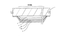
- FIG. 1 is a schematic cross-sectional view schematically showing a configuration of an organic EL element which is an embodiment of the present invention.
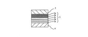
- FIG. 2 is a schematic cross-sectional view schematically showing a laminated structure of the organic EL element shown in FIG.
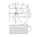
- FIG. 3 is a partial cross-sectional view of an organic EL device according to another embodiment of the present invention.
- FIG. 4 is a partial cross-sectional view of an organic EL device which is still another embodiment of the present invention.
- the organic EL device has a light-transmitting electrode layer 2, an organic layer 3, and a reflective metal electrode layer 4 on a light-transmitting substrate 1. They are stacked in order.
- the metal thin film CF in contact with the organic layer 3 and the plasmon loss preventing dielectric film TF constitute a reflective metal electrode layer 4 as a composite electrode.
- the metal thin film CF functions as a reflective cathode, and the plasmon loss prevention dielectric film TF functions as a plasmon loss prevention unit.
- the translucent material constituting the plasmon loss preventing dielectric film TF laminated on the metal thin film CF is an organic material such as a resin whose refractive index is equal to or higher than the refractive index of the organic layer 3, particularly the organic layer in contact with the metal thin film CF. Selected from materials.
- the plasmon loss preventing dielectric film TF is made of a hole transporting compound.
- “equivalent refractive index” means that the difference between one refractive index and the other refractive index is less than 0.3, preferably 0.2 or less, particularly preferably 0.1 or less. That means. Further, the refractive index “low” or “high” may be “low” or “high” to such an extent that a difference in measurement occurs, but in practice, it exceeds 0.1, preferably exceeds 0.2. More preferably 0.3 or more, still more preferably 0.4 or more, particularly preferably 0.5 or more, indicating a low or high difference.
- a sealing film 5 is formed on the plasmon loss preventing dielectric film TF to cover the organic film 3.
- the sealing film 5 seals the organic layer 3 and protects it from moisture and oxygen in the atmosphere.
- the sealing film 5 is formed of a single layer film such as an inorganic material such as silicon nitride, silicon oxide or silicon nitride carbide, or an organic material such as parylene, or a multilayer film in which an organic material layer and an organic material layer are alternately stacked. Can be done.
- the thickness of the organic layer 3 is set to, for example, 100 nm or more and 5 ⁇ m or less.
- the organic layer 3 sandwiched between the translucent electrode layer 2 and the reflective metal electrode layer is composed of a hole injection layer 3a, a hole transport layer 3b, a light emitting layer 3c, an electron stacked in order. It consists of a transport layer 3d and an electron injection layer 3e.
- the organic layer 3 is a light-emitting laminated body, and is not limited to these laminated structures, and may have a laminated structure including at least a light-emitting layer or a charge transport layer that can also be used.
- the organic layer 3 may be configured by omitting the hole transport layer 3b, the hole injection layer 3a, or the hole injection layer 3a and the electron transport layer 3d from the stacked structure. May be.
- Known methods for forming the organic layer 3 include dry coating methods such as sputtering and vacuum deposition, and wet coating methods such as screen printing, spraying, ink jetting, spin coating, gravure printing, and roll coater. ing.
- dry coating methods such as sputtering and vacuum deposition
- wet coating methods such as screen printing, spraying, ink jetting, spin coating, gravure printing, and roll coater.
- the hole injection layer, the hole transport layer, and the light emitting layer are uniformly formed as a solid film by a wet coating method
- the electron transport layer and the electron injection layer are uniformly formed sequentially as a solid film by a dry coating method.
- a film may be formed.
- all the functional layers may be uniformly and sequentially formed as a solid film by a wet coating method.
- the anode translucent electrode layer 2 for supplying holes to the functional layers up to the light emitting layer 3c is made of ITO (Indium-tin-oxide), ZnO, ZnO—Al 2 O 3 (so-called AZO), In 2 O 3. It can be composed of —ZnO (so-called IZO), SnO 2 —Sb 2 O 3 (so-called ATO), RuO 2 or the like. Furthermore, for the translucent electrode layer 2, it is preferable to select a material having a transmittance of at least 10% at the emission wavelength obtained from the organic EL material.
- the translucent electrode layer 2 usually has a single-layer structure, but it can also have a laminated structure made of a plurality of materials if desired.
- the cathode metal thin film CF that supplies electrons to the functional layers up to the light emitting layer 3c is not limited, but, for example, metals such as aluminum, silver, copper, nickel, chromium, gold, and platinum are used. In addition, these materials may be used only by 1 type and may use 2 or more types together by arbitrary combinations and a ratio.
- the material of the metal thin film CF preferably includes a metal having a low work function in order to perform electron injection efficiently.
- a metal having a low work function for example, an appropriate metal such as tin, magnesium, indium, calcium, aluminum, silver, or an alloy thereof may be used. Used. Specific examples include low work function alloy electrodes such as magnesium-silver alloy, magnesium-indium alloy, and aluminum-lithium alloy.
- the silver thin film with a thickness of 20 nm of the metal thin film CF has a transmittance of 50%.
- An Al film having a thickness of 10 nm as the metal thin film has a transmittance of 50%.
- the 20 nm-thick MgAg alloy film as the metal thin film has a transmittance of 50%.
- the metal thin film CF can be formed as a single layer film or a multilayer film on the organic layer 3 by a sputtering method, a vacuum deposition method or the like.
- the organic layer 3 is sandwiched between and in contact with the translucent electrode layer 2 and the metal thin film CF, the organic layer 3 is interposed between the translucent electrode layer 2 and the metal thin film CF.
- the light generated in the light emitting layer 3c in the organic layer 3 passes through the translucent electrode layer 2, and further passes through the translucent electrode layer 2 after being reflected by the metal thin film CF. Then, it is taken out from the surface of the translucent substrate 1.
- the hole injection layer 3a is preferably a layer containing an electron accepting compound (so-called hole transporting compound).
- the composition for forming a hole injection layer usually contains a hole transporting compound and a solvent as a constituent material of the hole injection layer.
- the solvent include, but are not limited to, ether solvents, ester solvents, aromatic hydrocarbon solvents, amide solvents, and the like.
- ether solvents include aliphatic ethers such as ethylene glycol dimethyl ether, ethylene glycol diethyl ether, propylene glycol monomethyl ether acetate (so-called PGMEA), 1,2-dimethoxybenzene, 1,3-dimethoxybenzene, anisole, and phenetole.
- Aromatic ethers such as 2-methoxytoluene, 3-methoxytoluene, 4-methoxytoluene, 2,3-dimethylanisole, and 2,4-dimethylanisole.
- ester solvent examples include aromatic esters such as phenyl acetate, phenyl propionate, methyl benzoate, ethyl benzoate, propyl benzoate, and n-butyl benzoate.
- aromatic hydrocarbon solvent examples include toluene, xylene, cyclohexylbenzene, 3- isopropylpropylphenyl, 1,2,3,4-tetramethylbenzene, 1,4-diisopropylbenzene, cyclohexylbenzene, methylnaphthalene and the like. Can be mentioned.
- amide solvent examples include N, N-dimethylformamide and N, N-dimethylacetamide.
- dimethyl sulfoxide and the like can also be used. These solvent may use only 1 type and may use 2 or more types by arbitrary combinations and a ratio.
- the hole transporting compound may be a polymer compound such as a polymer or a low molecular compound such as a monomer, but is preferably a low molecular compound.
- the hole transporting compound is preferably a compound having an ionization potential of 4.5 eV to 6.0 eV from the viewpoint of a charge injection barrier from the anode to the hole injection layer.
- hole transporting compounds include aromatic amine derivatives, phthalocyanine derivatives represented by phthalocyanine copper (so-called CuPc), porphyrin derivatives, oligothiophene derivatives, polythiophene derivatives, benzylphenyl derivatives, tertiary amines with fluorene groups.
- Examples include linked compounds, hydrazone derivatives, silazane derivatives, silanamine derivatives, phosphamine derivatives, quinacridone derivatives, polyaniline derivatives, polypyrrole derivatives, polyphenylene vinylene derivatives, polythienylene vinylene derivatives, polyquinoline derivatives, polyquinoxaline derivatives, and carbon.
- the derivative includes, for example, an aromatic amine derivative, and includes an aromatic amine itself and a compound having an aromatic amine as a main skeleton. There may be.
- a conductive polymer obtained by polymerizing 3,4-ethylenedioxythiophene, which is a polythiophene derivative, in high molecular weight polystyrene sulfonic acid is also preferable.
- the end of the polymer of PEDOT / PSS may be capped with methacrylate or the like.
- the hole transporting compound used as the material for the hole injection layer may contain any one of these compounds alone, or may contain two or more.
- the combination is arbitrary, but one or more kinds of aromatic tertiary amine polymer compounds and one or two kinds of other hole transporting compounds.
- an aromatic amine compound is preferable for the hole injection layer, and an aromatic tertiary amine compound is particularly preferable.
- the aromatic tertiary amine compound is a compound having an aromatic tertiary amine structure, and includes a compound having a group derived from an aromatic tertiary amine.
- the concentration of the hole transporting compound in the composition for forming a hole injection layer is usually 0.01% by weight or more, preferably 0.1% by weight or more, and more preferably 0.00% by weight in terms of film thickness uniformity. 5% by weight or more, usually 70% by weight or less, preferably 60% by weight or less, more preferably 50% by weight or less. If this concentration is too high, film thickness unevenness may occur, and if it is too low, defects may occur in the formed hole injection layer.
- the composition for forming a hole injection layer may further contain other components.
- other components include various organic EL materials, binder resins, coatability improvers, and the like.
- only 1 type may be used for another component and it may use 2 or more types together by arbitrary combinations and ratios.
- a material for forming the hole injection layer is mixed with an appropriate solvent to prepare a film-forming composition, and this hole injection layer forming composition
- the hole injection layer is formed by applying the material onto the anode by an appropriate technique, forming a film, and drying.
- the film thickness of the hole injection layer is usually 5 nm or more, preferably 10 nm or more, and usually 1000 nm or less, preferably 500 nm or less.
- the material of the hole transport layer 3b may be any material that has been conventionally used as a constituent material of the hole transport layer.
- it is exemplified as the hole transport compound used in the above-described hole injection layer. Things.
- polyvinylcarbazole derivatives polyarylamine derivatives, polyvinyltriphenylamine derivatives, polyfluorene derivatives, polyarylene derivatives, polyarylene ether sulfone derivatives containing tetraphenylbenzidine, polyarylene vinylene derivatives, polysiloxane derivatives, polythiophenes Derivatives, poly (p-phenylene vinylene) derivatives, and the like.
- These may be any of an alternating copolymer, a random polymer, a block polymer, or a graft copolymer. Further, it may be a polymer having a branched main chain and three or more terminal portions, or a so-called dendrimer.
- a composition for forming a hole transport layer is prepared in the same manner as the formation of the hole injection layer, and then dried after wet film formation.
- the hole transporting layer forming composition contains a solvent.
- the solvent used is the same as that used for the composition for forming the hole injection layer.
- the film forming conditions, the drying conditions, and the like are the same as in the case of forming the hole injection layer.
- the hole transport layer may contain various organic EL materials, a binder resin, a coating property improving agent and the like in addition to the hole transporting compound.
- the film thickness of the hole transport layer is usually 5 nm or more, preferably 10 nm or more, and usually 300 nm or less, preferably 100 nm or less.
- the film thickness of the hole injection layer 3a and / or the hole transport layer 3b from the anode 2 to the light emitting layer 3c is preferably at least 100 nm.
- the light emitting layer 3c may be a red, green and blue light emitting independent light emitting layer or a mixed light emitting layer thereof, a compound having a property of transporting holes (hole transporting compound), or A compound having an electron transporting property (electron transporting compound) can also be contained.
- An organic EL material may be used as a dopant material, and a hole transporting compound, an electron transporting compound, or the like may be appropriately used as a host material. There is no particular limitation on the organic EL material, and a substance that emits light at a desired emission wavelength and has good emission efficiency may be used.
- the organic EL material may be a fluorescent material or a phosphorescent material, but it is preferable to use a phosphorescent material from the viewpoint of internal quantum efficiency.
- the light emitting layer may have a single layer structure or a multilayer structure made of a plurality of materials as desired.
- a fluorescent material may be used for the blue light emitting layer
- a phosphorescent material may be used for the green and red light emitting layers.
- a diffusion preventing layer can be provided between the light emitting layers.
- fluorescent materials blue fluorescent dyes
- examples of fluorescent materials that emit blue light include naphthalene, perylene, pyrene, chrysene, anthracene, coumarin, p-bis (2-phenylethenyl) benzene, and derivatives thereof.
- fluorescent material green fluorescent dye
- examples of the fluorescent material (green fluorescent dye) that emits green light include aluminum complexes such as quinacridone derivatives, coumarin derivatives, and Alq3 (tris (8-hydroxy-quinoline) aluminum).
- Examples of fluorescent materials that give yellow light emission include rubrene and perimidone derivatives.
- red fluorescent dyes examples include DCM (4- (dicyanomethylene) -2-methyl-6- (p-dimethylaminostyryl) -4H-pyran) compounds, benzopyran derivatives, rhodamine derivatives, benzoates. Examples thereof include thioxanthene derivatives and azabenzothioxanthene.
- the phosphorescent material is selected from, for example, the long-period periodic table (hereinafter referred to as the long-period periodic table when referring to “periodic table” unless otherwise specified).
- An organometallic complex containing a metal can be given.
- Preferred examples of the metal selected from Groups 7 to 11 of the periodic table include ruthenium, rhodium, palladium, silver, rhenium, osmium, iridium, platinum, and gold.
- a ligand in which a (hetero) aryl group such as a (hetero) arylpyridine ligand or a (hetero) arylpyrazole ligand and a pyridine, pyrazole, phenanthroline, or the like is connected is preferable.
- a pyridine ligand and a phenylpyrazole ligand are preferable.
- (hetero) aryl represents an aryl group or a heteroaryl group.
- phosphorescent materials include tris (2-phenylpyridine) iridium (so-called Ir (ppy) 3), tris (2-phenylpyridine) ruthenium, tris (2-phenylpyridine) palladium, and bis (2-phenyl).
- Pyridine) platinum tris (2-phenylpyridine) osmium, tris (2-phenylpyridine) rhenium, octaethylplatinum porphyrin, octaphenylplatinum porphyrin, octaethyl palladium porphyrin, octaphenyl palladium porphyrin, and the like.
- the molecular weight of the compound used as the organic EL material is usually 10,000 or less, preferably 5000 or less, more preferably 4000 or less, still more preferably 3000 or less, and usually 100 or more, preferably 200 or more, more preferably 300 or more, still more preferably. Is in the range of 400 or more. If the molecular weight of the organic EL material is too small, the heat resistance will be significantly reduced, gas generation will be caused, the film quality will be deteriorated when the film is formed, or the morphology of the functional layer will be changed due to migration, etc. There is a case. On the other hand, if the molecular weight of the organic EL material is too large, it tends to be difficult to purify the organic compound, or it may take time to dissolve the organic EL material in a solvent when formed by a wet coating method.
- the proportion of the organic EL material in the light emitting layer is usually 0.05% by weight or more and usually 35% by weight or less. If the amount of the organic EL material is too small, uneven light emission may occur, and if the amount is too large, the light emission efficiency may be reduced. In addition, when using together 2 or more types of organic EL material, it is made for the total content of these to be contained in the said range.
- the component having the highest content in the light emitting layer is called a host material, and the component having a smaller content is called a guest material.
- the light emitting layer may contain a hole transporting compound as a constituent material.
- a hole transporting compound examples include various compounds exemplified as the hole transporting compound in the hole injection layer 3a described above, for example, Two or more condensed aromatic rings containing two or more tertiary amines represented by 4′-bis [N- (1-naphthyl) -N-phenylamino] biphenyl (so-called NPB) are attached to the nitrogen atom.
- Aromastituted aromatic diamines aromatic amine compounds having a starburst structure such as 4,4 ′, 4 ′′ -tris (1-naphthylphenylamino) triphenylamine, and aromatics composed of tetramers of triphenylamine And spiro compounds such as 2,2 ′, 7,7′-tetrakis- (diphenylamino) -9,9′-spirobifluorene.
- a hole transportable compound in a light emitting layer, only 1 type may be used for a hole transportable compound, and it may use 2 or more types together by arbitrary combinations and a ratio.
- the proportion of the hole transporting compound in the light emitting layer is usually 0.1% by weight or more and usually 65% by weight or less. If the amount of the hole transporting compound is too small, it may be easily affected by a short circuit, and if it is too large, the film thickness may be uneven. In addition, when using together 2 or more types of hole transportable compounds, it is made for the total content of these to be contained in the said range.
- the light emitting layer may contain an electron transporting compound as a constituent material.
- examples of low molecular weight electron transporting compounds include 2,5-bis (1-naphthyl) -1,3,4-oxadiazole (so-called BND), 2 , 5-bis (6 ′-(2 ′, 2 ′′ -bipyridyl))-1,1-dimethyl-3,4-diphenylsilole (so-called PyPySPyPy), bathophenanthroline (so-called BPhen), 2,9 -Dimethyl-4,7-diphenyl-1,10-phenanthroline (so-called BCP, bathocuproin), 2- (4-biphenylyl) -5- (p-tertiarybutylphenyl) -1,3,4-oxadiazole (So-called tBu-PBD), 4,4′-bis (9H-carbazol-9-yl) biphenyl (so-called BND),
- the proportion of the electron transporting compound in the light emitting layer is usually 0.1% by weight or more and usually 65% by weight or less. If the amount of the electron transporting compound is too small, it may be easily affected by a short circuit, and if it is too large, the film thickness may be uneven. In addition, when using together 2 or more types of electron transport compounds, it is made for the total content of these to be contained in the said range.
- the light emitting layer is prepared by dissolving the above light emitting layer material in an appropriate solvent to prepare a composition for forming a light emitting layer. Is formed. Therefore, in the case of forming by a wet coating method, the light emitting layer coating solution is prepared by dispersing or dissolving at least two kinds of solid contents (host material and guest material) to be the light emitting layer as a solute in a solvent.
- the solvent to be used can be selected from the solvents that can be used for the composition for forming a hole injection layer.
- the ratio of the light emitting layer solvent to the light emitting layer forming composition for forming the light emitting layer is usually 0.01% by weight or more and usually 70% by weight or less.
- the film thickness of the light emitting layer is usually 3 nm or more, preferably 5 nm or more, and usually 200 nm or less, preferably 100 nm or less. If the light emitting layer is too thin, defects may occur in the film, and if it is too thick, the driving voltage may increase.
- the electron transport layer 3d is provided for the purpose of further improving the light emission efficiency of the organic EL element, and efficiently transports electrons injected from the cathode between the electrodes to which an electric field is applied in the direction of the light emitting layer. It is formed from an electron transporting compound capable of forming
- the electron transporting compound used for the electron transporting layer usually, the electron injection efficiency from the cathode conductive film CF or the electron injection layer 3e is high, and the injected electrons with high electron mobility are efficiently used.
- a compound that can be transported is used. Examples of compounds that satisfy such conditions include metal complexes of Alq3 and 10-hydroxybenzo [h] quinoline, oxadiazole derivatives, distyrylbiphenyl derivatives, silole derivatives, 3-hydroxyflavone metal complexes, and 5-hydroxyflavones.
- Metal complex benzoxazole metal complex, benzothiazole metal complex, trisbenzimidazolylbenzene, quinoxaline compound, phenanthroline derivative, 2-t-butyl-9,10-N, N′-dicyanoanthraquinonediimine, n-type hydrogenated amorphous Quality silicon carbide, n-type zinc sulfide, n-type zinc selenide and the like.
- the formation method of the electron transport layer is not limited, and can be formed by a wet coating method or a dry coating method.
- the electron transport layer is prepared by dissolving the electron transport layer material in an appropriate solvent to prepare a composition for forming an electron transport layer. It is formed by removing.
- the solvent to be used can be selected from the solvents that can be used for the composition for forming a hole injection layer.
- the film thickness of the electron transport layer is usually 1 nm or more, preferably 5 nm or more, and usually 300 nm or less, preferably 100 nm or less.
- the electron injection layer 3e plays a role of efficiently injecting electrons injected from the cathode into the electron transport layer and the light emitting layer.
- the electron injection layer 3e includes organic electron transport compounds represented by metal complexes such as nitrogen-containing heterocyclic compounds such as bathophenanthroline and aluminum complexes of 8-hydroxyquinoline. Further, the electron injection efficiency can be increased by doping the electron injection layer 3e of the organic electron transport compound with an electron donating material.
- the electron donating material examples include alkali metals such as sodium and cesium, alkaline earth metals such as barium and calcium, compounds thereof (CsF, Cs 2 CO 3 , Li 2 O, LiF), sodium, Alkali metals such as potassium, cesium, lithium and rubidium are used.
- the thickness of the electron injection layer 3e is usually 5 nm or more, preferably 10 nm or more, and is usually 200 nm or less, preferably 100 nm or less.
- the formation method of the electron injection layer is not limited, and can be formed by a wet coating method or a dry coating method.
- the electron injection layer is prepared by dissolving the electron injection layer material in a suitable solvent to prepare a composition for forming an electron injection layer. It is formed by removing.
- the solvent to be used can be selected from the solvents that can be used for the composition for forming a hole injection layer.
- the distance between the light emitting point and the metal thin film CF functioning as the cathode is optically set to 3 times (odd times) of ⁇ / 4. That is, the light emitting layer 3c is designed so as to have a light emitting surface whose optical distance from the metal thin film CF is an odd multiple of three times or more of 1/4 of the light emission peak wavelength of the light emitting layer 3c.
- ⁇ / 4 140 and the refractive index is 1.8
- ⁇ 3 233
- the distance from the metal thin film CF to the emission center is 233 nm.
- the metal thin film CF is preferably disposed at a position separated from the light emitting surface by a half wavelength or more of the emission peak wavelength of the light emitting layer 3c.
- the refractive index between the light emitting layer side of the metal thin film CF and the outer plasmon loss prevention dielectric film side is equal to or higher, total reflection conditions are not satisfied at all angles within the circle indicated by the broken line, and evanescent light is not generated. There is no plasmon resonance.
- the evanescent light oozes from the high refractive index side to the low refractive index side at the time of total reflection, and the evanescent light oozed from the low refractive index layer with a thin film (thickness below wavelength) has a high refractive index on the outside. It has the property of returning to the original light. Further, the surface plasmon generated by the evanescent light and the light incident from a predetermined angle resonates (plasmon resonance), resulting in a plasmon loss, and the level of the reflected light rapidly decreases. However, no evanescent light is generated in this embodiment.
- light L3 within an obliquely upward critical angle passes through the hole transport layer 3b, the hole injection layer 3a, and the translucent electrode layer 2 as it is.
- Light L4 having a critical angle or more at the interface between the translucent electrode layer 2 and the glass substrate proceeds while repeatedly attenuated total reflection.
- light L5 obliquely below proceeds as it is from the time of light emission and reaches the metal thin film CF. Plasmon resonance is prevented because the plasmon loss preventing dielectric film TF is used. Also in this case, evanescent light is not generated and plasmon resonance does not occur.
- the downward light L6 does not generate evanescent light, and is reflected by the metal thin film CF so that the optical path length is ⁇ / 4. Furthermore, because of the metal reflection at the metal thin film CF, the phase is further shifted by ⁇ , and eventually the light has the same phase as the emitted light. Therefore, because the phase is the same as that of the upward light, they are output in an intensified manner.
- the metal thin film CF is disposed at a position far from the light emitting layer 3c, that is, 3 ⁇ ⁇ / 4, and the plasmon loss preventing dielectric film TF having a refractive index equal to or higher than that of the organic layer on the opposite side of the metal thin film CF. Therefore, it is possible to obtain an effect of reducing loss during light emission and suppressing plasmon loss.
- the cathode when the cathode is composed only of a thin film metal and the outside is made into the atmosphere or inert gas, the cathode emits light in all directions from the light emitting layer having a refractive index of 1.8.
- the light directed toward is totally reflected by the cathode at a critical angle or more in relation to the refractive index of 1.0 outside the cathode, and evanescent light is generated.
- the evanescent light oozes with an amplitude that decreases exponentially in a direction perpendicular to the cathode plane. Then, surface plasmons are excited by evanescent light on the side opposite to the light extraction of the metal cathode.
- the metal thin film CF is Ag
- resonance occurs at a predetermined angle when the film thickness is 20 nm to 80 nm.
- the degree of absorption differs depending on the film thickness, and the absorption is greatest when the film thickness is about 50 nm.
- the film thickness is 20 nm or less, polarization is not sufficient and incident light is transmitted.
- a dielectric plasmon loss prevention dielectric film TF is laminated on an Ag metal thin film CF having a thickness of 50 nm to prevent generation of surface plasmon by Ag absorption and resonance with evanescent light. .
- the refractive index of the plasmon loss preventing dielectric film TF equal to or higher than the refractive index of the light emitting layer, total reflection by the metal-dielectric material does not occur and evanescent light does not occur.
- the light from the metal thin film CF is reflected and can be extracted without plasmon loss.
- FIG. 4 shows a partial cross-sectional view of the organic EL element according to the second embodiment.
- symbol as the said Example is the same as that of the organic EL element of the said Example, those description is abbreviate
- the plasmon loss prevention dielectric film TF is laminated on the metal thin film CF on the side opposite to the light extraction to prevent plasmon resonance.
- the metal thin film CF can be configured as a multilayer.
- the cathode in contact with the organic layer 3 is composed of two layers, for example, a thin Ag metal thin film main body CF1 and an Al protective metal film CF2 laminated thereon, and further a protective metal film CF2 A plasmon loss preventing dielectric film TF is laminated thereon.
- the protective metal film CF2 is set to a thickness at which evanescent light attenuates.
- the Ag metal thin film main body CF1 has a film thickness of 20 nm to 80 nm, the influence of plasmon resonance starts to appear at the film thickness of 20 nm, and the maximum is the metal thin film main body CF1 per 50 nm of film thickness. Since the thickness at which the plasmon resonance is considerably reduced is 80 nm, the minimum value of the total thickness of the metal thin film main body CF1 is 80 nm.
- the range in which the evanescent light on the dielectric TF side of the surface plasmon reaches is also about 300 nm, and it is preferable that the total film thickness of the metal thin film body CF1 and the protective metal film CF2 in which the influence change is reduced is, for example, up to 200 nm. .
- the amplitude of the surface plasmon attenuates exponentially, but the attenuation distance (distance that becomes 1 / e of the amplitude) attenuates more rapidly on the metal side than on the dielectric side.
- the film thickness of the metal thin film body CF1 can be made thinner than the film thickness of the protective metal film CF2.
- the resin solvent may adversely affect the organic material of the organic layer 3, but according to the second embodiment, the protective metal film CF2 is formed. Since it is installed between the metal thin film body CF1 and the plasmon loss preventing dielectric film TF, the influence can be mitigated.
- the protective metal film CF2 in contact with the cathode for example, the Ag metal thin film body CF1 can be made of low-cost Al, Mg, Cr, or the like. Therefore, since the metal thin film main body can be made thin, an organic EL element that does not cause plasmon loss while maintaining performance at low cost can be provided. In addition, since no current flows through the protective metal film CF2, there is no fear of contact with different metals and corrosion in a corrosive environment. In the case of this configuration, the protective metal film CF2 may be grounded.
- a quartz or glass plate, a metal plate or metal foil, a bent resin substrate, a plastic film, a sheet, or the like is used as the translucent substrate 1.
- a glass plate or a transparent plate made of a synthetic resin such as polyester, polymethacrylate, polycarbonate, or polysulfone is preferable.
- a synthetic resin substrate it is necessary to pay attention to gas barrier properties. If the gas barrier property of the substrate is too small, the organic EL element may be deteriorated by the outside air that has passed through the substrate. Therefore, a method of securing a gas barrier property by providing a dense silicon oxide film or the like on at least one surface of the synthetic resin substrate is also a preferable method.
- the organic layer is a light emitting laminate, but the light emitting laminate can also be configured by lamination of inorganic material films.
Landscapes
- Engineering & Computer Science (AREA)
- Manufacturing & Machinery (AREA)
- Electroluminescent Light Sources (AREA)
Priority Applications (1)
| Application Number | Priority Date | Filing Date | Title |
|---|---|---|---|
| PCT/JP2012/065739 WO2013190656A1 (fr) | 2012-06-20 | 2012-06-20 | Élément électroluminescent organique |
Applications Claiming Priority (1)
| Application Number | Priority Date | Filing Date | Title |
|---|---|---|---|
| PCT/JP2012/065739 WO2013190656A1 (fr) | 2012-06-20 | 2012-06-20 | Élément électroluminescent organique |
Publications (1)
| Publication Number | Publication Date |
|---|---|
| WO2013190656A1 true WO2013190656A1 (fr) | 2013-12-27 |
Family
ID=49768285
Family Applications (1)
| Application Number | Title | Priority Date | Filing Date |
|---|---|---|---|
| PCT/JP2012/065739 Ceased WO2013190656A1 (fr) | 2012-06-20 | 2012-06-20 | Élément électroluminescent organique |
Country Status (1)
| Country | Link |
|---|---|
| WO (1) | WO2013190656A1 (fr) |
Cited By (1)
| Publication number | Priority date | Publication date | Assignee | Title |
|---|---|---|---|---|
| JP2016061852A (ja) * | 2014-09-16 | 2016-04-25 | セイコーエプソン株式会社 | 波長変換素子、光源装置、およびプロジェクター |
Citations (8)
| Publication number | Priority date | Publication date | Assignee | Title |
|---|---|---|---|---|
| JPH11220171A (ja) * | 1998-02-02 | 1999-08-10 | Toyoda Gosei Co Ltd | 窒化ガリウム系化合物半導体素子 |
| JP2000243573A (ja) * | 1999-02-18 | 2000-09-08 | Pioneer Electronic Corp | 有機エレクトロルミネッセンス素子とその製造方法 |
| JP2007157514A (ja) * | 2005-12-06 | 2007-06-21 | Sony Corp | 表示装置 |
| JP2008543074A (ja) * | 2005-06-03 | 2008-11-27 | コーニンクレッカ フィリップス エレクトロニクス エヌ ヴィ | 有機エレクトロルミネッセント光源 |
| WO2011043083A1 (fr) * | 2009-10-09 | 2011-04-14 | 出光興産株式会社 | Élément organique électroluminescent |
| JP2011521423A (ja) * | 2008-05-23 | 2011-07-21 | エルジー・ケム・リミテッド | 有機発光素子およびその製造方法 |
| JP2011198540A (ja) * | 2010-03-18 | 2011-10-06 | Canon Inc | 表示装置 |
| JP2012094812A (ja) * | 2010-09-28 | 2012-05-17 | Toyoda Gosei Co Ltd | Iii族窒化物半導体発光素子の製造方法 |
-
2012
- 2012-06-20 WO PCT/JP2012/065739 patent/WO2013190656A1/fr not_active Ceased
Patent Citations (8)
| Publication number | Priority date | Publication date | Assignee | Title |
|---|---|---|---|---|
| JPH11220171A (ja) * | 1998-02-02 | 1999-08-10 | Toyoda Gosei Co Ltd | 窒化ガリウム系化合物半導体素子 |
| JP2000243573A (ja) * | 1999-02-18 | 2000-09-08 | Pioneer Electronic Corp | 有機エレクトロルミネッセンス素子とその製造方法 |
| JP2008543074A (ja) * | 2005-06-03 | 2008-11-27 | コーニンクレッカ フィリップス エレクトロニクス エヌ ヴィ | 有機エレクトロルミネッセント光源 |
| JP2007157514A (ja) * | 2005-12-06 | 2007-06-21 | Sony Corp | 表示装置 |
| JP2011521423A (ja) * | 2008-05-23 | 2011-07-21 | エルジー・ケム・リミテッド | 有機発光素子およびその製造方法 |
| WO2011043083A1 (fr) * | 2009-10-09 | 2011-04-14 | 出光興産株式会社 | Élément organique électroluminescent |
| JP2011198540A (ja) * | 2010-03-18 | 2011-10-06 | Canon Inc | 表示装置 |
| JP2012094812A (ja) * | 2010-09-28 | 2012-05-17 | Toyoda Gosei Co Ltd | Iii族窒化物半導体発光素子の製造方法 |
Cited By (1)
| Publication number | Priority date | Publication date | Assignee | Title |
|---|---|---|---|---|
| JP2016061852A (ja) * | 2014-09-16 | 2016-04-25 | セイコーエプソン株式会社 | 波長変換素子、光源装置、およびプロジェクター |
Similar Documents
| Publication | Publication Date | Title |
|---|---|---|
| KR102122188B1 (ko) | 유기 전계 발광 소자 및 유기 전계 발광 디바이스 | |
| JP5884213B2 (ja) | 有機電界発光素子の製造方法、有機電界発光素子、有機elディスプレイ及び有機el照明 | |
| JP6062954B2 (ja) | ミラー装置 | |
| JP2015050095A (ja) | 機能層形成用インクの製造方法、有機el素子の製造方法 | |
| JP6046738B2 (ja) | ミラー装置 | |
| JP2009212510A (ja) | 有機電界発光素子、有機elディスプレイおよび有機el照明 | |
| JP2009266814A (ja) | 有機電界発光素子の製造方法、有機電界発光素子、有機elディスプレイ及び有機el照明 | |
| KR20140112500A (ko) | 유기 전계 발광 소자, 유기 el 조명 및 유기 el 표시 장치 | |
| JP5912174B2 (ja) | 有機エレクトロルミネッセンスパネル及びその製造方法 | |
| JP2010209320A (ja) | 有機電界発光素子用組成物、有機電界発光素子の製造方法、有機電界発光素子、有機elディスプレイ及び有機el照明 | |
| JP6433963B2 (ja) | ミラー装置 | |
| JP5402703B2 (ja) | 有機電界発光素子、有機elディスプレイ、有機el照明及び有機el信号装置 | |
| WO2012090560A1 (fr) | Élément électroluminescent organique et son procédé de fabrication | |
| JP6185109B2 (ja) | 有機エレクトロルミネッセンスパネル及びその製造方法 | |
| WO2013190656A1 (fr) | Élément électroluminescent organique | |
| WO2013190620A1 (fr) | Élément électroluminescent organique | |
| JP5527105B2 (ja) | 成膜用インク、成膜方法および発光素子の製造方法 | |
| WO2013150593A1 (fr) | Panneau électroluminescent organique et son procédé de fabrication | |
| WO2012176276A1 (fr) | Élément électroluminescent organique à champ électrique | |
| WO2014073072A1 (fr) | Dispositif miroir | |
| JP5527104B2 (ja) | 成膜用インク、成膜方法および発光素子の製造方法 | |
| JP2010192474A (ja) | 有機電界発光素子、有機elディスプレイ及び有機el照明 | |
| JP6340404B2 (ja) | 発光装置 | |
| JP2018117035A (ja) | 有機エレクトロルミネッセンス素子 | |
| JP2010239008A (ja) | 有機電界発光素子、有機elディスプレイ及び有機el照明 |
Legal Events
| Date | Code | Title | Description |
|---|---|---|---|
| 121 | Ep: the epo has been informed by wipo that ep was designated in this application |
Ref document number: 12879413 Country of ref document: EP Kind code of ref document: A1 |
|
| NENP | Non-entry into the national phase |
Ref country code: DE |
|
| 122 | Ep: pct application non-entry in european phase |
Ref document number: 12879413 Country of ref document: EP Kind code of ref document: A1 |
|
| NENP | Non-entry into the national phase |
Ref country code: JP |