WO2014057748A1 - Substrat composite à nitrure du groupe iii, procédé pour sa fabrication et procédé de fabrication d'un dispositif semi-conducteur à nitrure du groupe iii - Google Patents
Substrat composite à nitrure du groupe iii, procédé pour sa fabrication et procédé de fabrication d'un dispositif semi-conducteur à nitrure du groupe iii Download PDFInfo
- Publication number
- WO2014057748A1 WO2014057748A1 PCT/JP2013/073805 JP2013073805W WO2014057748A1 WO 2014057748 A1 WO2014057748 A1 WO 2014057748A1 JP 2013073805 W JP2013073805 W JP 2013073805W WO 2014057748 A1 WO2014057748 A1 WO 2014057748A1
- Authority
- WO
- WIPO (PCT)
- Prior art keywords
- group iii
- iii nitride
- substrate
- nitride film
- film
- Prior art date
- Legal status (The legal status is an assumption and is not a legal conclusion. Google has not performed a legal analysis and makes no representation as to the accuracy of the status listed.)
- Ceased
Links
Images








Classifications
-
- H—ELECTRICITY
- H10—SEMICONDUCTOR DEVICES; ELECTRIC SOLID-STATE DEVICES NOT OTHERWISE PROVIDED FOR
- H10P—GENERIC PROCESSES OR APPARATUS FOR THE MANUFACTURE OR TREATMENT OF DEVICES COVERED BY CLASS H10
- H10P14/00—Formation of materials, e.g. in the shape of layers or pillars
- H10P14/20—Formation of materials, e.g. in the shape of layers or pillars of semiconductor materials
- H10P14/32—Formation of materials, e.g. in the shape of layers or pillars of semiconductor materials characterised by intermediate layers between substrates and deposited layers
- H10P14/3242—Structure
- H10P14/3256—Microstructure
-
- H—ELECTRICITY
- H10—SEMICONDUCTOR DEVICES; ELECTRIC SOLID-STATE DEVICES NOT OTHERWISE PROVIDED FOR
- H10P—GENERIC PROCESSES OR APPARATUS FOR THE MANUFACTURE OR TREATMENT OF DEVICES COVERED BY CLASS H10
- H10P90/00—Preparation of wafers not covered by a single main group of this subclass, e.g. wafer reinforcement
- H10P90/19—Preparing inhomogeneous wafers
- H10P90/1904—Preparing vertically inhomogeneous wafers
- H10P90/1906—Preparing SOI wafers
- H10P90/1914—Preparing SOI wafers using bonding
- H10P90/1916—Preparing SOI wafers using bonding with separation or delamination along an ion implanted layer, e.g. Smart-cut
-
- B—PERFORMING OPERATIONS; TRANSPORTING
- B32—LAYERED PRODUCTS
- B32B—LAYERED PRODUCTS, i.e. PRODUCTS BUILT-UP OF STRATA OF FLAT OR NON-FLAT, e.g. CELLULAR OR HONEYCOMB, FORM
- B32B7/00—Layered products characterised by the relation between layers; Layered products characterised by the relative orientation of features between layers, or by the relative values of a measurable parameter between layers, i.e. products comprising layers having different physical, chemical or physicochemical properties; Layered products characterised by the interconnection of layers
- B32B7/04—Interconnection of layers
-
- H—ELECTRICITY
- H10—SEMICONDUCTOR DEVICES; ELECTRIC SOLID-STATE DEVICES NOT OTHERWISE PROVIDED FOR
- H10P—GENERIC PROCESSES OR APPARATUS FOR THE MANUFACTURE OR TREATMENT OF DEVICES COVERED BY CLASS H10
- H10P14/00—Formation of materials, e.g. in the shape of layers or pillars
- H10P14/20—Formation of materials, e.g. in the shape of layers or pillars of semiconductor materials
- H10P14/29—Formation of materials, e.g. in the shape of layers or pillars of semiconductor materials characterised by the substrates
- H10P14/2901—Materials
-
- H—ELECTRICITY
- H10—SEMICONDUCTOR DEVICES; ELECTRIC SOLID-STATE DEVICES NOT OTHERWISE PROVIDED FOR
- H10P—GENERIC PROCESSES OR APPARATUS FOR THE MANUFACTURE OR TREATMENT OF DEVICES COVERED BY CLASS H10
- H10P14/00—Formation of materials, e.g. in the shape of layers or pillars
- H10P14/20—Formation of materials, e.g. in the shape of layers or pillars of semiconductor materials
- H10P14/29—Formation of materials, e.g. in the shape of layers or pillars of semiconductor materials characterised by the substrates
- H10P14/2901—Materials
- H10P14/2907—Materials being Group IIIA-VA materials
- H10P14/2908—Nitrides
-
- H—ELECTRICITY
- H10—SEMICONDUCTOR DEVICES; ELECTRIC SOLID-STATE DEVICES NOT OTHERWISE PROVIDED FOR
- H10P—GENERIC PROCESSES OR APPARATUS FOR THE MANUFACTURE OR TREATMENT OF DEVICES COVERED BY CLASS H10
- H10P14/00—Formation of materials, e.g. in the shape of layers or pillars
- H10P14/20—Formation of materials, e.g. in the shape of layers or pillars of semiconductor materials
- H10P14/29—Formation of materials, e.g. in the shape of layers or pillars of semiconductor materials characterised by the substrates
- H10P14/2901—Materials
- H10P14/2921—Materials being crystalline insulating materials
-
- H—ELECTRICITY
- H10—SEMICONDUCTOR DEVICES; ELECTRIC SOLID-STATE DEVICES NOT OTHERWISE PROVIDED FOR
- H10P—GENERIC PROCESSES OR APPARATUS FOR THE MANUFACTURE OR TREATMENT OF DEVICES COVERED BY CLASS H10
- H10P14/00—Formation of materials, e.g. in the shape of layers or pillars
- H10P14/20—Formation of materials, e.g. in the shape of layers or pillars of semiconductor materials
- H10P14/29—Formation of materials, e.g. in the shape of layers or pillars of semiconductor materials characterised by the substrates
- H10P14/2901—Materials
- H10P14/2922—Materials being non-crystalline insulating materials, e.g. glass or polymers
-
- H—ELECTRICITY
- H10—SEMICONDUCTOR DEVICES; ELECTRIC SOLID-STATE DEVICES NOT OTHERWISE PROVIDED FOR
- H10P—GENERIC PROCESSES OR APPARATUS FOR THE MANUFACTURE OR TREATMENT OF DEVICES COVERED BY CLASS H10
- H10P14/00—Formation of materials, e.g. in the shape of layers or pillars
- H10P14/20—Formation of materials, e.g. in the shape of layers or pillars of semiconductor materials
- H10P14/29—Formation of materials, e.g. in the shape of layers or pillars of semiconductor materials characterised by the substrates
- H10P14/2924—Structures
- H10P14/2925—Surface structures
-
- H—ELECTRICITY
- H10—SEMICONDUCTOR DEVICES; ELECTRIC SOLID-STATE DEVICES NOT OTHERWISE PROVIDED FOR
- H10P—GENERIC PROCESSES OR APPARATUS FOR THE MANUFACTURE OR TREATMENT OF DEVICES COVERED BY CLASS H10
- H10P14/00—Formation of materials, e.g. in the shape of layers or pillars
- H10P14/20—Formation of materials, e.g. in the shape of layers or pillars of semiconductor materials
- H10P14/32—Formation of materials, e.g. in the shape of layers or pillars of semiconductor materials characterised by intermediate layers between substrates and deposited layers
-
- H—ELECTRICITY
- H10—SEMICONDUCTOR DEVICES; ELECTRIC SOLID-STATE DEVICES NOT OTHERWISE PROVIDED FOR
- H10P—GENERIC PROCESSES OR APPARATUS FOR THE MANUFACTURE OR TREATMENT OF DEVICES COVERED BY CLASS H10
- H10P14/00—Formation of materials, e.g. in the shape of layers or pillars
- H10P14/20—Formation of materials, e.g. in the shape of layers or pillars of semiconductor materials
- H10P14/34—Deposited materials, e.g. layers
- H10P14/3451—Structure
- H10P14/3452—Microstructure
-
- H—ELECTRICITY
- H10—SEMICONDUCTOR DEVICES; ELECTRIC SOLID-STATE DEVICES NOT OTHERWISE PROVIDED FOR
- H10P—GENERIC PROCESSES OR APPARATUS FOR THE MANUFACTURE OR TREATMENT OF DEVICES COVERED BY CLASS H10
- H10P90/00—Preparation of wafers not covered by a single main group of this subclass, e.g. wafer reinforcement
- H10P90/19—Preparing inhomogeneous wafers
- H10P90/1904—Preparing vertically inhomogeneous wafers
- H10P90/1906—Preparing SOI wafers
- H10P90/1914—Preparing SOI wafers using bonding
-
- H—ELECTRICITY
- H10—SEMICONDUCTOR DEVICES; ELECTRIC SOLID-STATE DEVICES NOT OTHERWISE PROVIDED FOR
- H10P—GENERIC PROCESSES OR APPARATUS FOR THE MANUFACTURE OR TREATMENT OF DEVICES COVERED BY CLASS H10
- H10P90/00—Preparation of wafers not covered by a single main group of this subclass, e.g. wafer reinforcement
- H10P90/19—Preparing inhomogeneous wafers
- H10P90/1904—Preparing vertically inhomogeneous wafers
- H10P90/1906—Preparing SOI wafers
- H10P90/1922—Preparing SOI wafers using silicon etch back techniques, e.g. BESOI or ELTRAN
-
- H—ELECTRICITY
- H10—SEMICONDUCTOR DEVICES; ELECTRIC SOLID-STATE DEVICES NOT OTHERWISE PROVIDED FOR
- H10W—GENERIC PACKAGES, INTERCONNECTIONS, CONNECTORS OR OTHER CONSTRUCTIONAL DETAILS OF DEVICES COVERED BY CLASS H10
- H10W10/00—Isolation regions in semiconductor bodies between components of integrated devices
- H10W10/10—Isolation regions comprising dielectric materials
- H10W10/181—Semiconductor-on-insulator [SOI] isolation regions, e.g. buried oxide regions of SOI wafers
-
- B—PERFORMING OPERATIONS; TRANSPORTING
- B32—LAYERED PRODUCTS
- B32B—LAYERED PRODUCTS, i.e. PRODUCTS BUILT-UP OF STRATA OF FLAT OR NON-FLAT, e.g. CELLULAR OR HONEYCOMB, FORM
- B32B2307/00—Properties of the layers or laminate
- B32B2307/20—Properties of the layers or laminate having particular electrical or magnetic properties, e.g. piezoelectric
-
- B—PERFORMING OPERATIONS; TRANSPORTING
- B32—LAYERED PRODUCTS
- B32B—LAYERED PRODUCTS, i.e. PRODUCTS BUILT-UP OF STRATA OF FLAT OR NON-FLAT, e.g. CELLULAR OR HONEYCOMB, FORM
- B32B7/00—Layered products characterised by the relation between layers; Layered products characterised by the relative orientation of features between layers, or by the relative values of a measurable parameter between layers, i.e. products comprising layers having different physical, chemical or physicochemical properties; Layered products characterised by the interconnection of layers
- B32B7/04—Interconnection of layers
- B32B7/06—Interconnection of layers permitting easy separation
-
- H—ELECTRICITY
- H10—SEMICONDUCTOR DEVICES; ELECTRIC SOLID-STATE DEVICES NOT OTHERWISE PROVIDED FOR
- H10D—INORGANIC ELECTRIC SEMICONDUCTOR DEVICES
- H10D62/00—Semiconductor bodies, or regions thereof, of devices having potential barriers
- H10D62/80—Semiconductor bodies, or regions thereof, of devices having potential barriers characterised by the materials
- H10D62/85—Semiconductor bodies, or regions thereof, of devices having potential barriers characterised by the materials being Group III-V materials, e.g. GaAs
- H10D62/8503—Nitride Group III-V materials, e.g. AlN or GaN
-
- H—ELECTRICITY
- H10—SEMICONDUCTOR DEVICES; ELECTRIC SOLID-STATE DEVICES NOT OTHERWISE PROVIDED FOR
- H10H—INORGANIC LIGHT-EMITTING SEMICONDUCTOR DEVICES HAVING POTENTIAL BARRIERS
- H10H20/00—Individual inorganic light-emitting semiconductor devices having potential barriers, e.g. light-emitting diodes [LED]
- H10H20/01—Manufacture or treatment
- H10H20/011—Manufacture or treatment of bodies, e.g. forming semiconductor layers
- H10H20/013—Manufacture or treatment of bodies, e.g. forming semiconductor layers having light-emitting regions comprising only Group III-V materials
- H10H20/0133—Manufacture or treatment of bodies, e.g. forming semiconductor layers having light-emitting regions comprising only Group III-V materials with a substrate not being Group III-V materials
- H10H20/01335—Manufacture or treatment of bodies, e.g. forming semiconductor layers having light-emitting regions comprising only Group III-V materials with a substrate not being Group III-V materials the light-emitting regions comprising nitride materials
-
- H—ELECTRICITY
- H10—SEMICONDUCTOR DEVICES; ELECTRIC SOLID-STATE DEVICES NOT OTHERWISE PROVIDED FOR
- H10H—INORGANIC LIGHT-EMITTING SEMICONDUCTOR DEVICES HAVING POTENTIAL BARRIERS
- H10H20/00—Individual inorganic light-emitting semiconductor devices having potential barriers, e.g. light-emitting diodes [LED]
- H10H20/01—Manufacture or treatment
- H10H20/011—Manufacture or treatment of bodies, e.g. forming semiconductor layers
- H10H20/018—Bonding of wafers
-
- H—ELECTRICITY
- H10—SEMICONDUCTOR DEVICES; ELECTRIC SOLID-STATE DEVICES NOT OTHERWISE PROVIDED FOR
- H10H—INORGANIC LIGHT-EMITTING SEMICONDUCTOR DEVICES HAVING POTENTIAL BARRIERS
- H10H20/00—Individual inorganic light-emitting semiconductor devices having potential barriers, e.g. light-emitting diodes [LED]
- H10H20/80—Constructional details
- H10H20/81—Bodies
- H10H20/815—Bodies having stress relaxation structures, e.g. buffer layers
-
- H—ELECTRICITY
- H10—SEMICONDUCTOR DEVICES; ELECTRIC SOLID-STATE DEVICES NOT OTHERWISE PROVIDED FOR
- H10H—INORGANIC LIGHT-EMITTING SEMICONDUCTOR DEVICES HAVING POTENTIAL BARRIERS
- H10H20/00—Individual inorganic light-emitting semiconductor devices having potential barriers, e.g. light-emitting diodes [LED]
- H10H20/80—Constructional details
- H10H20/81—Bodies
- H10H20/8215—Bodies characterised by crystalline imperfections, e.g. dislocations; characterised by the distribution of dopants, e.g. delta-doping
-
- H—ELECTRICITY
- H10—SEMICONDUCTOR DEVICES; ELECTRIC SOLID-STATE DEVICES NOT OTHERWISE PROVIDED FOR
- H10P—GENERIC PROCESSES OR APPARATUS FOR THE MANUFACTURE OR TREATMENT OF DEVICES COVERED BY CLASS H10
- H10P14/00—Formation of materials, e.g. in the shape of layers or pillars
- H10P14/20—Formation of materials, e.g. in the shape of layers or pillars of semiconductor materials
- H10P14/29—Formation of materials, e.g. in the shape of layers or pillars of semiconductor materials characterised by the substrates
-
- H—ELECTRICITY
- H10—SEMICONDUCTOR DEVICES; ELECTRIC SOLID-STATE DEVICES NOT OTHERWISE PROVIDED FOR
- H10P—GENERIC PROCESSES OR APPARATUS FOR THE MANUFACTURE OR TREATMENT OF DEVICES COVERED BY CLASS H10
- H10P14/00—Formation of materials, e.g. in the shape of layers or pillars
- H10P14/20—Formation of materials, e.g. in the shape of layers or pillars of semiconductor materials
- H10P14/32—Formation of materials, e.g. in the shape of layers or pillars of semiconductor materials characterised by intermediate layers between substrates and deposited layers
- H10P14/3202—Materials thereof
- H10P14/3214—Materials thereof being Group IIIA-VA semiconductors
- H10P14/3216—Nitrides
-
- H—ELECTRICITY
- H10—SEMICONDUCTOR DEVICES; ELECTRIC SOLID-STATE DEVICES NOT OTHERWISE PROVIDED FOR
- H10P—GENERIC PROCESSES OR APPARATUS FOR THE MANUFACTURE OR TREATMENT OF DEVICES COVERED BY CLASS H10
- H10P14/00—Formation of materials, e.g. in the shape of layers or pillars
- H10P14/20—Formation of materials, e.g. in the shape of layers or pillars of semiconductor materials
- H10P14/34—Deposited materials, e.g. layers
- H10P14/3402—Deposited materials, e.g. layers characterised by the chemical composition
- H10P14/3414—Deposited materials, e.g. layers characterised by the chemical composition being group IIIA-VIA materials
- H10P14/3416—Nitrides
-
- H—ELECTRICITY
- H10—SEMICONDUCTOR DEVICES; ELECTRIC SOLID-STATE DEVICES NOT OTHERWISE PROVIDED FOR
- H10P—GENERIC PROCESSES OR APPARATUS FOR THE MANUFACTURE OR TREATMENT OF DEVICES COVERED BY CLASS H10
- H10P14/00—Formation of materials, e.g. in the shape of layers or pillars
- H10P14/20—Formation of materials, e.g. in the shape of layers or pillars of semiconductor materials
- H10P14/36—Formation of materials, e.g. in the shape of layers or pillars of semiconductor materials characterised by treatments done before the formation of the materials
-
- H—ELECTRICITY
- H10—SEMICONDUCTOR DEVICES; ELECTRIC SOLID-STATE DEVICES NOT OTHERWISE PROVIDED FOR
- H10P—GENERIC PROCESSES OR APPARATUS FOR THE MANUFACTURE OR TREATMENT OF DEVICES COVERED BY CLASS H10
- H10P52/00—Grinding, lapping or polishing of wafers, substrates or parts of devices
- H10P52/40—Chemomechanical polishing [CMP]
- H10P52/402—Chemomechanical polishing [CMP] of semiconductor materials
-
- H—ELECTRICITY
- H10—SEMICONDUCTOR DEVICES; ELECTRIC SOLID-STATE DEVICES NOT OTHERWISE PROVIDED FOR
- H10P—GENERIC PROCESSES OR APPARATUS FOR THE MANUFACTURE OR TREATMENT OF DEVICES COVERED BY CLASS H10
- H10P72/00—Handling or holding of wafers, substrates or devices during manufacture or treatment thereof
- H10P72/70—Handling or holding of wafers, substrates or devices during manufacture or treatment thereof for supporting or gripping
- H10P72/74—Handling or holding of wafers, substrates or devices during manufacture or treatment thereof for supporting or gripping using temporarily an auxiliary support
-
- H—ELECTRICITY
- H10—SEMICONDUCTOR DEVICES; ELECTRIC SOLID-STATE DEVICES NOT OTHERWISE PROVIDED FOR
- H10P—GENERIC PROCESSES OR APPARATUS FOR THE MANUFACTURE OR TREATMENT OF DEVICES COVERED BY CLASS H10
- H10P72/00—Handling or holding of wafers, substrates or devices during manufacture or treatment thereof
- H10P72/70—Handling or holding of wafers, substrates or devices during manufacture or treatment thereof for supporting or gripping
- H10P72/74—Handling or holding of wafers, substrates or devices during manufacture or treatment thereof for supporting or gripping using temporarily an auxiliary support
- H10P72/7424—Handling or holding of wafers, substrates or devices during manufacture or treatment thereof for supporting or gripping using temporarily an auxiliary support used as a support during the manufacture of self-supporting substrates
-
- H—ELECTRICITY
- H10—SEMICONDUCTOR DEVICES; ELECTRIC SOLID-STATE DEVICES NOT OTHERWISE PROVIDED FOR
- H10P—GENERIC PROCESSES OR APPARATUS FOR THE MANUFACTURE OR TREATMENT OF DEVICES COVERED BY CLASS H10
- H10P72/00—Handling or holding of wafers, substrates or devices during manufacture or treatment thereof
- H10P72/70—Handling or holding of wafers, substrates or devices during manufacture or treatment thereof for supporting or gripping
- H10P72/74—Handling or holding of wafers, substrates or devices during manufacture or treatment thereof for supporting or gripping using temporarily an auxiliary support
- H10P72/744—Details of chemical or physical process used for separating the auxiliary support from a device or a wafer
-
- H—ELECTRICITY
- H10—SEMICONDUCTOR DEVICES; ELECTRIC SOLID-STATE DEVICES NOT OTHERWISE PROVIDED FOR
- H10P—GENERIC PROCESSES OR APPARATUS FOR THE MANUFACTURE OR TREATMENT OF DEVICES COVERED BY CLASS H10
- H10P90/00—Preparation of wafers not covered by a single main group of this subclass, e.g. wafer reinforcement
- H10P90/12—Preparing bulk and homogeneous wafers
- H10P90/129—Preparing bulk and homogeneous wafers by polishing
-
- Y—GENERAL TAGGING OF NEW TECHNOLOGICAL DEVELOPMENTS; GENERAL TAGGING OF CROSS-SECTIONAL TECHNOLOGIES SPANNING OVER SEVERAL SECTIONS OF THE IPC; TECHNICAL SUBJECTS COVERED BY FORMER USPC CROSS-REFERENCE ART COLLECTIONS [XRACs] AND DIGESTS
- Y10—TECHNICAL SUBJECTS COVERED BY FORMER USPC
- Y10T—TECHNICAL SUBJECTS COVERED BY FORMER US CLASSIFICATION
- Y10T428/00—Stock material or miscellaneous articles
- Y10T428/24—Structurally defined web or sheet [e.g., overall dimension, etc.]
- Y10T428/24273—Structurally defined web or sheet [e.g., overall dimension, etc.] including aperture
- Y10T428/24298—Noncircular aperture [e.g., slit, diamond, rectangular, etc.]
-
- Y—GENERAL TAGGING OF NEW TECHNOLOGICAL DEVELOPMENTS; GENERAL TAGGING OF CROSS-SECTIONAL TECHNOLOGIES SPANNING OVER SEVERAL SECTIONS OF THE IPC; TECHNICAL SUBJECTS COVERED BY FORMER USPC CROSS-REFERENCE ART COLLECTIONS [XRACs] AND DIGESTS
- Y10—TECHNICAL SUBJECTS COVERED BY FORMER USPC
- Y10T—TECHNICAL SUBJECTS COVERED BY FORMER US CLASSIFICATION
- Y10T428/00—Stock material or miscellaneous articles
- Y10T428/24—Structurally defined web or sheet [e.g., overall dimension, etc.]
- Y10T428/24273—Structurally defined web or sheet [e.g., overall dimension, etc.] including aperture
- Y10T428/24322—Composite web or sheet
-
- Y—GENERAL TAGGING OF NEW TECHNOLOGICAL DEVELOPMENTS; GENERAL TAGGING OF CROSS-SECTIONAL TECHNOLOGIES SPANNING OVER SEVERAL SECTIONS OF THE IPC; TECHNICAL SUBJECTS COVERED BY FORMER USPC CROSS-REFERENCE ART COLLECTIONS [XRACs] AND DIGESTS
- Y10—TECHNICAL SUBJECTS COVERED BY FORMER USPC
- Y10T—TECHNICAL SUBJECTS COVERED BY FORMER US CLASSIFICATION
- Y10T428/00—Stock material or miscellaneous articles
- Y10T428/24—Structurally defined web or sheet [e.g., overall dimension, etc.]
- Y10T428/24273—Structurally defined web or sheet [e.g., overall dimension, etc.] including aperture
- Y10T428/24322—Composite web or sheet
- Y10T428/24331—Composite web or sheet including nonapertured component
-
- Y—GENERAL TAGGING OF NEW TECHNOLOGICAL DEVELOPMENTS; GENERAL TAGGING OF CROSS-SECTIONAL TECHNOLOGIES SPANNING OVER SEVERAL SECTIONS OF THE IPC; TECHNICAL SUBJECTS COVERED BY FORMER USPC CROSS-REFERENCE ART COLLECTIONS [XRACs] AND DIGESTS
- Y10—TECHNICAL SUBJECTS COVERED BY FORMER USPC
- Y10T—TECHNICAL SUBJECTS COVERED BY FORMER US CLASSIFICATION
- Y10T428/00—Stock material or miscellaneous articles
- Y10T428/24—Structurally defined web or sheet [e.g., overall dimension, etc.]
- Y10T428/24942—Structurally defined web or sheet [e.g., overall dimension, etc.] including components having same physical characteristic in differing degree
- Y10T428/2495—Thickness [relative or absolute]
-
- Y—GENERAL TAGGING OF NEW TECHNOLOGICAL DEVELOPMENTS; GENERAL TAGGING OF CROSS-SECTIONAL TECHNOLOGIES SPANNING OVER SEVERAL SECTIONS OF THE IPC; TECHNICAL SUBJECTS COVERED BY FORMER USPC CROSS-REFERENCE ART COLLECTIONS [XRACs] AND DIGESTS
- Y10—TECHNICAL SUBJECTS COVERED BY FORMER USPC
- Y10T—TECHNICAL SUBJECTS COVERED BY FORMER US CLASSIFICATION
- Y10T428/00—Stock material or miscellaneous articles
- Y10T428/24—Structurally defined web or sheet [e.g., overall dimension, etc.]
- Y10T428/24942—Structurally defined web or sheet [e.g., overall dimension, etc.] including components having same physical characteristic in differing degree
- Y10T428/2495—Thickness [relative or absolute]
- Y10T428/24967—Absolute thicknesses specified
- Y10T428/24975—No layer or component greater than 5 mils thick
-
- Y—GENERAL TAGGING OF NEW TECHNOLOGICAL DEVELOPMENTS; GENERAL TAGGING OF CROSS-SECTIONAL TECHNOLOGIES SPANNING OVER SEVERAL SECTIONS OF THE IPC; TECHNICAL SUBJECTS COVERED BY FORMER USPC CROSS-REFERENCE ART COLLECTIONS [XRACs] AND DIGESTS
- Y10—TECHNICAL SUBJECTS COVERED BY FORMER USPC
- Y10T—TECHNICAL SUBJECTS COVERED BY FORMER US CLASSIFICATION
- Y10T428/00—Stock material or miscellaneous articles
- Y10T428/26—Web or sheet containing structurally defined element or component, the element or component having a specified physical dimension
-
- Y—GENERAL TAGGING OF NEW TECHNOLOGICAL DEVELOPMENTS; GENERAL TAGGING OF CROSS-SECTIONAL TECHNOLOGIES SPANNING OVER SEVERAL SECTIONS OF THE IPC; TECHNICAL SUBJECTS COVERED BY FORMER USPC CROSS-REFERENCE ART COLLECTIONS [XRACs] AND DIGESTS
- Y10—TECHNICAL SUBJECTS COVERED BY FORMER USPC
- Y10T—TECHNICAL SUBJECTS COVERED BY FORMER US CLASSIFICATION
- Y10T428/00—Stock material or miscellaneous articles
- Y10T428/26—Web or sheet containing structurally defined element or component, the element or component having a specified physical dimension
- Y10T428/263—Coating layer not in excess of 5 mils thick or equivalent
- Y10T428/264—Up to 3 mils
- Y10T428/265—1 mil or less
-
- Y—GENERAL TAGGING OF NEW TECHNOLOGICAL DEVELOPMENTS; GENERAL TAGGING OF CROSS-SECTIONAL TECHNOLOGIES SPANNING OVER SEVERAL SECTIONS OF THE IPC; TECHNICAL SUBJECTS COVERED BY FORMER USPC CROSS-REFERENCE ART COLLECTIONS [XRACs] AND DIGESTS
- Y10—TECHNICAL SUBJECTS COVERED BY FORMER USPC
- Y10T—TECHNICAL SUBJECTS COVERED BY FORMER US CLASSIFICATION
- Y10T428/00—Stock material or miscellaneous articles
- Y10T428/31—Surface property or characteristic of web, sheet or block
Definitions
- the present invention relates to a group III nitride composite substrate and a method for manufacturing the same, and a method for manufacturing a group III nitride semiconductor device using the group III nitride composite substrate.
- Group III nitride semiconductors such as GaN, AlN, and Al x Ga 1-x N (0 ⁇ x ⁇ 1) have excellent semiconductor characteristics and are therefore suitable as substrates for semiconductor devices. Since such a group III nitride semiconductor is expensive, from the viewpoint of reducing the manufacturing cost of the semiconductor device, as a substrate of the semiconductor device, a group III nitride semiconductor such as GaN or AlN is formed on a support substrate such as a silicon substrate. A semiconductor substrate on which a film is formed has been proposed.
- Patent Document 1 discloses a step of implanting ions in the vicinity of the surface of a first nitride semiconductor substrate made of GaN or AlN, and the surface of the first nitride semiconductor substrate. A step of superimposing the second substrate on the side, a step of heat-treating the two superimposed substrates, and a portion of the first nitride semiconductor substrate on the second layer with the ion-implanted layer as a boundary.
- a method for manufacturing a semiconductor substrate comprising a step of peeling off from a substrate.
- a semiconductor substrate obtained by the method for manufacturing a semiconductor substrate disclosed in Japanese Patent Application Laid-Open No. 2006-210660 has a thin film thickness of about 2 ⁇ m of a nitride semiconductor formed on a support substrate. There is a problem that the sheet resistance is increased, and there is a problem that a yield is lowered due to partial resistance increase due to damage caused by ion implantation.
- the present invention solves the above-described problems, and provides a group III nitride composite substrate having a low sheet resistance obtained with a high yield, a method for manufacturing the same, and a group III nitride semiconductor device using the group III nitride composite substrate It aims to provide a method.
- the group III nitride composite substrate includes a group III nitride film and a support substrate formed of a material having a chemical composition different from that of the group III nitride film.
- the group III nitride film is bonded to the support substrate in either a direct or indirect form.
- the thickness of the group III nitride film is 10 ⁇ m or more, and the sheet resistance on the main surface on the group III nitride film side is 200 ⁇ / sq (ohms per square) or less.
- the thickness of the group III nitride film is 10 ⁇ m or more, the sheet resistance on the main surface on the group III nitride film side can be lowered to 200 ⁇ / sq or less, and a high yield can be achieved.
- a group III nitride semiconductor device can be manufactured.
- the area of the bonding region between the group III nitride film and the support substrate is 70% or more of the area of the main surface, and the non-group between the group III nitride film and the support substrate
- the joining region includes at least one non-joining partial region, and the non-joining partial region can be a small non-joining partial region having a maximum diameter of less than 20 mm.
- the area of the junction region is as large as 70% or more of the area of the main surface, and the maximum diameter of the non-joint partial region constituting the non-joint region is small and less than 20 mm.
- a physical semiconductor device can be manufactured.
- the non-joining region between the group III nitride film and the support substrate includes at least one non-joining partial region, and the non-joining partial region is in contact with the outer periphery of the main surface. There can be no inner non-bonded partial area.
- the non-joining partial region constituting the non-joining region is not in contact with the outer periphery of the main surface, so that the group III nitride semiconductor device can be manufactured with a high yield.
- the group III nitride film has a main surface through hole, and the area of the main surface through hole can be 10% or less of the area of the main surface.
- the area of the main surface through hole of the group III nitride film is 10% or less of the area of the main surface, so that a group III nitride semiconductor device can be manufactured with a high yield.
- the junction interface between the group III nitride film and the support substrate contains an impurity including a metal, and the impurity concentration may be 1 ⁇ 10 10 cm ⁇ 2 or more. it can.
- the concentration of impurities including a metal at the bonding interface is 1 ⁇ 10 10 cm ⁇ 2 or more. Therefore, the group III nitride semiconductor device can be manufactured with high bonding strength and high yield. it can.
- the thermal expansion coefficient of the group III nitride film can be made larger than 0.7 times and smaller than 1.4 times compared with the thermal expansion coefficient of the supporting substrate.
- Such a group III nitride composite substrate has a group III nitride film having a thermal expansion coefficient larger than 0.7 times and smaller than 1.4 times compared with the thermal expansion coefficient of the support substrate.
- the group III nitride semiconductor device can be manufactured with a high yield by suppressing the occurrence of warpage and / or cracks.
- the fracture toughness of the supporting substrate and 1MNm -2/3 or more, the thickness of the supporting substrate may be equal to or larger than 50 [mu] m. Since the group III nitride composite substrate has high mechanical strength, a group III nitride semiconductor device can be manufactured with a high yield.
- the indirect form may be a form in which a bonding film is interposed between the group III nitride film and the support substrate.
- the group III nitride film and the support substrate are bonded together with a bonding film interposed between them, so that the bonding strength is high and the group III nitride is high in yield.
- Semiconductor devices can be manufactured.
- a method for producing a group III nitride composite substrate according to another aspect of the present invention is a method for producing a group III nitride composite substrate according to the above aspect, wherein the group III nitride film and the support substrate are directly and indirectly connected. And a step of reducing the thickness of at least one of the bonded group III nitride film and the supporting substrate.
- Such a method for producing a group III nitride composite substrate includes the above-described steps, whereby a group III nitride composite substrate having a high yield and a low sheet resistance can be produced.
- a method for producing a group III nitride semiconductor device is a method for producing a group III nitride semiconductor device using a group III nitride composite substrate according to the above aspect, comprising a group III nitride composite substrate And a step of growing at least one group III nitride layer on the main surface of the group III nitride composite substrate on the group III nitride film side.
- Such a group III nitride semiconductor device manufacturing method includes the above-described steps, whereby a group III nitride semiconductor device can be manufactured with a high yield.
- the present invention it is possible to provide a group III nitride composite substrate having a low sheet resistance obtained with a high yield, a method for manufacturing the same, and a method for manufacturing a group III nitride semiconductor device using the group III nitride composite substrate.
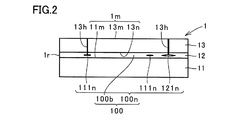
- a group III nitride composite substrate 1 is formed of a group III nitride film 13 and a material having a chemical composition different from that of group III nitride film 13. Supporting substrate 11.
- the group III nitride film 13 is bonded to the support substrate 11 in either a direct or indirect form.
- the thickness of the group III nitride film 13 is 10 ⁇ m or more.
- the sheet resistance on the main surface 13m on the group III nitride film 13 side is 200 ⁇ / sq or less.
- the sheet resistance on the main surface 13 m on the group III nitride film 13 side is as low as 200 ⁇ / sq or less.
- a group III nitride semiconductor device can be manufactured with a high yield. Details will be described below.
- the group III nitride composite substrate 1 of this embodiment includes a group III nitride film 13 and a support substrate 11 formed of a material having a chemical composition different from that of the group III nitride film 13.
- the group III nitride film 13 refers to a substrate formed of a semiconductor that is a compound of at least one group III element and nitrogen.
- the manufacturing method of the group III nitride film 13 is not particularly limited, and examples of the vapor phase method include an HVPE (hydride vapor phase growth) method and a sublimation method. Examples of the liquid phase method include a high nitrogen pressure solution method and a flux. Law.
- the group III nitride film 13 is preferably a crystal and more preferably a single crystal from the viewpoint of growing a group III nitride layer having high crystal quality on the group III nitride film 13.
- the group III nitride film 13 can be doped with a conductivity improving impurity in order to reduce the sheet resistance.
- conductivity improving impurities are not particularly limited, but O (oxygen) atoms, Si (silicon) atoms, and the like are preferable from the viewpoint of a high effect of improving conductivity.
- the support substrate 11 refers to a substrate that supports the group III nitride film 13 and is not particularly limited as long as it is formed of a material having a chemical composition different from that of the group III nitride film 13.
- oxide substrates sapphire substrates and other Al 2 O 3 substrates, mullite substrates and other Al 2 O 3 —SiO 2 based substrates, spinel substrates and other Al 2 O 3 —MgO based substrates, Al 2 O 3 And —SiO 2 —YSZ (yttria stabilized zirconia) based substrate.
- the metal substrate include a Mo substrate, a W substrate, and a Cu—W substrate.
- the group III nitride film 13 is a GaN film
- a substrate formed of AlN, which is a group III nitride having a chemical composition different from that of GaN may be used.
- the support substrate 11 may be crystalline or non-crystalline, and if it is a crystal, it may be a single crystal or a polycrystal.
- the group III nitride film 13 is bonded to the support substrate 11 in either a direct or indirect form.
- “bonded in a direct form” means that group III nitride film 13 and support substrate 11 are directly bonded without interposing another one therebetween. That means.
- the bonding interface 100 is a surface formed by the main surface 13n of the group III nitride film 13 and the main surface 11m of the support substrate 11 bonded to each other.
- “indirectly bonded” means that the group III nitride film 13 and the support substrate 11 are indirectly connected with another, for example, a bonding film 12 interposed therebetween. It means being joined.
- the bonding interface differs as follows depending on the bonding method.
- the bonding film 12 a is formed on the main surface 11 m of the support substrate 11 and the bonding film 12 b is formed on the main surface 13 n of the group III nitride film 13.
- the bonding interface Reference numeral 100 denotes a surface formed by the main surface 12am of the bonding film 12a and the main surface 12bn of the bonding film 12b inside the bonding film 12 bonded to each other.
- the bonding interface 100 is a surface formed by the main surface of the bonding film 12 and the main surface 13n of the group III nitride film 13 that are bonded to each other.
- the bonding interface 100 is a surface formed by the main surface of the bonding film 12 and the main surface 11m of the support substrate 11 that are bonded to each other.
- the bonding film 12 that can be included between the group III nitride film 13 and the support substrate 11 of the group III nitride composite substrate 1 of the present embodiment has a high bonding strength between the group III nitride film 13 and the support substrate 11.
- SiO 2 film, Si 3 N 4 film, AlN film, Al 2 O 3 film, TiO 2 film, TiN film, Ga 2 O 3 film, W film, Mo film, Au— Sn film etc. are mentioned.
- the thickness of the bonding film 12 is not particularly limited, but is preferably 0.05 ⁇ m or more, more preferably 0.1 ⁇ m or more from the viewpoint of increasing the bonding strength between the group III nitride film 13 and the support substrate 11. From the viewpoint of improving the in-plane uniformity and flatness of the bonding film 12, the thickness is preferably 5 ⁇ m or less, more preferably 2 ⁇ m or less.
- the thickness of the group III nitride film 13 needs to be 10 ⁇ m or more from the viewpoint of reducing the sheet resistance on the main surface 13m on the group III nitride film 13 side. 50 ⁇ m or more is preferable, and 100 ⁇ m or more is more preferable. Further, from the viewpoint of reducing the cost of the group III nitride composite substrate 1, the thickness of the group III nitride film 13 is preferably 500 ⁇ m or less, and more preferably 250 ⁇ m or less.
- the group III nitride composite substrate 1 of the present embodiment has the device characteristics of a group III nitride semiconductor device obtained by reducing the sheet resistance of the group III nitride composite substrate 1 (for example, the light emission efficiency of the light emitting device). From the viewpoint of increasing, the sheet resistance on the main surface 13m on the group III nitride film 13 needs to be 200 ⁇ / sq (ohms per square) or less, preferably 50 ⁇ / sq or less, and more preferably 10 ⁇ / sq or less.
- a group III nitride film 13 is bonded to the support substrate 11 at the bonding interface 100 described above. Also in the group III nitride composite substrate 1 of the present embodiment, the support substrate 11, the group III nitride film 13, and the bonding films 12, 12a, and 12b are similar to the group III nitride composite substrate manufactured by the ion implantation method.
- the surface roughness of the main surface, the main surface through-hole 13h of the group III nitride film 13 and the non-uniformity of bonding are present. Therefore, also in the group III nitride composite substrate 1 of the present embodiment, at the bonding interface 100, the bonding region 100b in which the group III nitride film 13 and the support substrate 11 are bonded either directly or indirectly. And a non-bonded region 100n where the group III nitride film 13 and the support substrate 11 are not bonded directly or indirectly.
- the presence, position, size, and area of the bonding region 100b and the non-bonding region 100n at the bonding interface 100 of the group III nitride composite substrate 1 of the present embodiment are determined using an ultrasonic microscope, a defect evaluation apparatus, or the like. Can be measured.
- the non-bonding region 100n in the bonding interface 100 of the group III nitride composite substrate 1 of the present embodiment includes at least one non-bonding partial region 111n, 112n, 121n, 122n.
- the non-junction partial regions 111n, 112n, 121n, and 122n have an indefinite shape but are substantially circular or elliptical, and therefore the size is evaluated based on the maximum diameter (maximum diameter). From the viewpoint of size, the non-joint partial regions 111n, 112n, 121n, and 122n are small non-joint partial regions 111n, 112n having a maximum diameter of less than 20 mm and large non-joint portions having a maximum diameter of 20 mm or more.
- the regions 121n and 122n can be classified.
- the non-joint partial regions 111n, 112n, 121n, and 122n are the inner non-joint partial regions 111n and 121n that are not in contact with the outer periphery 1r of the main surface 1m, and the regions are the main, from the viewpoint of the existence position. It can be classified into outer non-joined partial regions 112n and 122n in contact with the outer periphery 1r of the surface 1m.
- the group III nitride composite substrate 1 of the present embodiment has an area of the junction region 100b between the group III nitride film 13 and the support substrate 11 of 1 m on the main surface.
- the area is preferably 70% or more, more preferably 85% or more.
- the group III nitride film 13 and the support substrate are manufactured in the process of manufacturing the group III nitride semiconductor device. 11 is easily separated, and it is difficult to increase the yield of the group III nitride semiconductor device.
- the non-joint partial region is a small non-joint partial region 111n, 112n whose maximum diameter is less than 20 mm. It is preferable that That is, in FIG. 3, the non-joining partial regions are preferably small non-joining partial regions 111n and 112n.
- the group III nitride composite substrate 1 of the present embodiment has a non-bonded partial region that is not in contact with the outer periphery 1r of the main surface 1m.
- the partial regions 111n and 121n are preferable. That is, in FIG. 3, it is preferable that the non-joining partial regions are inner non-joining partial regions 111n and 121n.
- the group III nitride composite substrate 1 including the outer non-junction partial regions 112n and 122n is a group III nitride semiconductor device in the process of manufacturing the group III nitride composite substrate 1 and using the group III nitride composite substrate 1 During the manufacturing process, contaminants enter the bonding interface 100, and it is difficult to clean and remove the contaminants. Therefore, it is difficult to increase the yield of the group III nitride semiconductor device. Further, the group III nitride composite substrate 1 including the outer non-bonded partial regions 112n and 122n is being processed in the process of reducing the thickness of at least one of the group III nitride film 13 and the support substrate 11 bonded together. Therefore, it is difficult to increase the yield of the group III nitride semiconductor device.
- the non-joint partial region is more preferably a small and inner non-joint partial region 111n from the viewpoint of manufacturing a group III nitride semiconductor device with a high yield. That is, in FIG. 3, it is more preferable that the non-joining partial regions are small and inner non-joining partial regions 111n.
- group III nitride composite substrate 1 of the present embodiment includes a main surface through hole of group III nitride film 13 from the viewpoint of manufacturing a group III nitride semiconductor device with a high yield.
- the area of 13h is preferably 10% or less, and more preferably 5% or less with respect to the areas of the main surfaces 1m and 13m.
- the main surface through-hole 13h refers to the main surface of the group III nitride film 13 that is directly or indirectly bonded to the support substrate 11 and another surface (specifically, another main surface and A hole penetrating between the side surfaces.
- a non-bonding region 100n is formed on the main surface through hole 13h and in the vicinity thereof. Further, in the step of manufacturing the group III nitride semiconductor device, when the group III nitride semiconductor device is cleaned, the cleaning agent enters the bonding interface via the main surface through hole 13h, so that the group III nitride is obtained. The bonding strength of the composite substrate 1 may decrease. If the area of main surface through-hole 13h is larger than 10% of the area of main surface 1m, the area of non-junction region 100n increases, and it becomes difficult to increase the yield of group III nitride semiconductor devices.
- the group III nitride composite substrate 1 of the present embodiment has a group III nitride film 13 from the viewpoint of manufacturing a group III nitride semiconductor device with a high yield by increasing the bonding strength.
- the concentration of impurities including a metal contained in the bonding interface 100 between the support substrate 11 and the support substrate 11 is preferably 1 ⁇ 10 10 cm ⁇ 2 or more, and more preferably 1.5 ⁇ 10 10 cm ⁇ 2 or more. .
- the impurities including metal are not particularly limited, but from the viewpoint of increasing the bonding strength, when the group III nitride composite substrate 1 includes an oxide film such as a SiO 2 film as the bonding film 12, Fe (iron), Ni Base metal oxides such as (nickel) which have a higher ionization tendency than H (hydrogen) and are easily oxidized are preferred.
- the group III nitride composite substrate 1 of the present embodiment has a high yield by suppressing the occurrence of warpage and / or cracks during the manufacture of a group III nitride semiconductor device.
- the thermal expansion coefficient of the group III nitride film 13 is preferably greater than 0.7 times and smaller than 1.4 times the thermal expansion coefficient of the support substrate 11. 0.75 times or more and 1.25 times or less is more preferable.
- the group III nitride composite substrate 1 of the present embodiment is provided with a support substrate from the viewpoint of suppressing the occurrence of warpage and / or cracks during the manufacture of a group III nitride semiconductor device.
- fracture toughness is preferably not 1MNm -2/3 or more, more preferably 1.5MNm -2/3 or more.
- the thickness of the support substrate is preferably 50 ⁇ m or more, more preferably 100 ⁇ m or more.
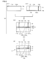
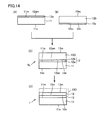
- the method for manufacturing group III nitride composite substrate 1 according to another embodiment of the present invention is the method for manufacturing group III nitride composite substrate 1 according to the first embodiment. Then, the step of bonding the group III nitride film 13 and the support substrate 11 in a direct or indirect form (FIG. 4A), the group III nitride film 13 and the support substrate 11 And a step of reducing at least one thickness (FIG. 4B).
- the manufacturing method of the group III nitride composite substrate 1 of this embodiment can manufacture a group III nitride composite substrate having a high yield and a low sheet resistance by including the above steps.
- Step of bonding group III nitride film and supporting substrate With reference to FIGS. 1, 2, and 4, in the method of manufacturing group III nitride composite substrate 1 of this embodiment, first, group III nitride film 13 and support substrate 11 are directly and indirectly bonded. In any form, the process of bonding is included.
- the group III nitride film 13 and the support substrate 11 are bonded together in a direct form means that the group III nitride film 13 and the support substrate 11 are directly connected without interposing any other material therebetween. It means sticking together.
- bonding the group III nitride film 13 and the support substrate 11 in an indirect form means that the group III nitride film 13 and the support substrate 11 are sandwiched between them, for example, a bonding film 12. Indirect bonding.
- the method of bonding the group III nitride film 13 and the support substrate 11 is not particularly limited in any of the direct and indirect bonding modes, and after the bonded surfaces are washed and bonded as they are, 600 Direct bonding method in which bonding is performed by raising the temperature to about °C to 1200 °C, and the surface to be bonded in a low temperature atmosphere of room temperature (for example, 25 °C) to about 400 °C after cleaning the bonded surfaces and activating with plasma or ions Activated bonding method, after the bonded surface is cleaned with a chemical solution and pure water, and then the high pressure bonding method in which a high pressure of about 0.1 MPa to 10 MPa is applied and after the bonded surface is cleaned with a chemical solution and pure water A high vacuum bonding method in which bonding is performed in a high vacuum atmosphere of about 10 ⁇ 6 Pa to 10 ⁇ 3 Pa is suitable.
- the bonding strength can be further increased by raising the temperature to about 600 ° C. to 1200 ° C. after the bonding.
- the effect of increasing the bonding strength by raising the temperature to about 600 ° C. to 1200 ° C. after the bonding is large.
- the group III nitride film 13 and the support substrate 11 can be bonded in any of the direct and indirect forms as described above, but from the viewpoint of increasing the bonding strength, FIG. As shown in A), it is preferable that the group III nitride film 13 and the support substrate 11 are bonded indirectly with a bonding film 12 interposed therebetween. Details will be described below.
- the step of indirectly bonding the group III nitride film 13 and the support substrate 11 with the bonding film 12 interposed therebetween is performed on the main surface 11m of the support substrate 11.
- a sub-process for forming 12a (FIG. 4A1), a sub-process for forming the bonding film 12b on the main surface 13n of the group III nitride film 13 (FIG. 4A2), and a main surface of the support substrate 11.
- the bonding film 12a and the bonding film 12b bonded together are integrated by bonding to form the bonding film 12, and the support substrate 11 and the group III nitride film 13 interpose the bonding film 12. Let them join.
- the surface roughness of the main surface of the support substrate 11, the group III nitride film 13, and the bonding films 12, 12a, 12b, the group III nitride film 13 are bonded either directly or indirectly at the bonding interface 100 due to the presence of the main surface through-hole 13h and the non-uniformity of the bonding.
- Region 100b, and non-bonded region 100n where group III nitride film 13 and support substrate 11 are not directly or indirectly bonded are formed.
- the bonding region 100b and the non-bonding region 100n are as described above.
- the method for forming the bonding films 12a and 12b is not particularly limited, but from the viewpoint of suppressing the film formation cost, a sputtering method, a vapor deposition method, a CVD (chemical vapor deposition) method, or the like is preferably performed. Further, the method for bonding the supporting substrate 11 and the group III nitride film 13 by bonding the bonding film 12a and the bonding film 12b is not particularly limited. As described above, the direct bonding method and the surface activation are performed. A bonding method, a high pressure bonding method, a high vacuum bonding method, or the like is preferable.
- Step of reducing the thickness of at least one of the group III nitride film and the supporting substrate Referring to FIG. 4B, in the manufacturing method of group III nitride composite substrate 1 of the present embodiment, the thickness of at least one of group III nitride film 13 and support substrate 11 bonded together is then determined. And making it smaller.
- the method of reducing the thickness of at least one of the group III nitride film 13 and the support substrate 11 is not particularly limited, and is a method of cutting the substrate to be reduced in thickness parallel to the main surface, Examples thereof include a method for grinding and / or polishing a surface, a method for etching a main surface, and a method using a laser.
- the method using a laser is a method of irradiating a laser beam such that the focal point of the laser beam is located at a predetermined depth from the main surface of the substrate.
- the substrate can be separated in the region by changing the chemical composition of the region where the laser beam is focused at a predetermined depth from the main surface of the substrate.
- a femtosecond laser from the viewpoint of changing the chemical composition of a region at a predetermined depth from the main surface of the substrate and not changing the chemical composition of a region other than the above region, a femtosecond laser, A second laser is preferably used.
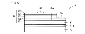
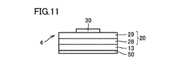
- the manufacturing method of group III nitride semiconductor device 4 which is still another embodiment of the present invention includes a step of preparing group III nitride composite substrate 1, Growing at least one group III nitride layer 20 on the main surface 13m on the group III nitride film 13 side.
- the manufacturing method of the group III nitride semiconductor device 4 of this embodiment can manufacture a group III nitride semiconductor device with a high yield by providing said process.
- the manufacturing method of the group III nitride semiconductor device 4 of the present embodiment first includes a step of preparing the group III nitride composite substrate 1.
- the step of preparing the group III nitride composite substrate 1 is the same as the step in the method for manufacturing the group III nitride composite substrate 1 of the second embodiment.
- Step of growing group III nitride layer In the method of manufacturing the group III nitride semiconductor device 4 of the present embodiment, at least one group III nitride layer 20 is then formed on the main surface 13m of the group III nitride composite substrate 1 on the group III nitride film 13 side. Including a growth step.
- the method for growing the group III nitride layer 20 is not particularly limited, but from the viewpoint of growing the group III nitride layer 20 with high crystal quality, as a vapor phase method, an MOCVD (metal organic chemical vapor deposition) method, An MBE (molecular beam growth) method, an HVPE (hydride vapor phase epitaxy) method, a sublimation method, and the like are preferable.
- a vapor phase method an MOCVD (metal organic chemical vapor deposition) method, An MBE (molecular beam growth) method, an HVPE (hydride vapor phase epitaxy) method, a sublimation method, and the like are preferable.
- a liquid phase method a high nitrogen pressure solution method, a flux method, and the like are preferable.
- the structure of the group III nitride layer 20 to be grown differs depending on the type and function of the group III nitride semiconductor device.
- the group III nitride semiconductor device 4 is a light emitting device
- the first conductivity type GaN layer is formed as the group III nitride layer 20 on the main surface 13m of the group III nitride composite substrate 1 on the group III nitride film 13 side.
- first conductivity type Al s Ga 1-s N layer 202 (where s is 0 ⁇ s ⁇ 1)
- light emitting layer 203
- second conductivity type Al t Ga 1-t N layer 204 (where t 0 ⁇ t ⁇ 1)
- the second conductivity type GaN layer 205 can be grown in this order.
- the manufacturing method of the group III nitride semiconductor device 4 of this embodiment can then include a step of forming electrodes (first electrode and second electrode).
- a part of each of the second conductivity type GaN layer 204, the light emitting layer 203, the first conductivity type Al s Ga 1-s N layer 202, and the first conductivity type GaN layer 201 is mesoscopic. By removing by etching, a part of the first conductivity type GaN layer 201 is exposed.
- the first electrode 31 can be formed on the exposed main surface of the first conductivity type GaN layer 201, and the second electrode can be formed on the exposed main surface of the second conductivity type GaN layer.
- the formation method of the first electrode 31 and the second electrode 32 is not particularly limited, and examples thereof include a CVD (chemical vapor deposition) method, a sputtering method, and a vapor deposition method.
- Reference invention I is a group III nitride composite substrate having a group III nitride film having a low cost, a large diameter, a large film thickness, a small film thickness distribution, and a high crystal quality, a method for manufacturing the same, and a laminated group III nitride composite substrate And a group III nitride semiconductor device and a method for manufacturing the same.
- Group III nitrides such as GaN are suitably used for semiconductor devices because they have excellent semiconductor properties.
- Japanese Patent Laid-Open No. 2009-126722 discloses a self-standing group III nitride substrate having a diameter of 25 mm or more and 160 mm or more and a thickness of 100 ⁇ m or more and 1000 ⁇ m or less as a semiconductor device substrate, as a specific example, a diameter of 100 mm and a thickness.
- a self-standing GaN substrate having a thickness of 400 ⁇ m is disclosed.
- Japanese Patent Application Laid-Open No. 2008-010766 discloses a heterogeneous substrate having a chemical composition different from that of GaN as a substrate for manufacturing a semiconductor device, and a GaN thin film having a thickness of 0.1 ⁇ m or more and 100 ⁇ m or less bonded to the heterogeneous substrate. And a GaN thin film bonded substrate having a diameter of 50.8 mm in which a sapphire substrate and a GaN thin film having a thickness of 0.1 ⁇ m or 100 ⁇ m are bonded as a specific example. .
- Japanese Unexamined Patent Application Publication No. 2010-182936 discloses a composite substrate including a support substrate, a nitride semiconductor layer, and a bonding layer provided between the support substrate and the nitride semiconductor layer as a semiconductor device substrate.
- a composite substrate is disclosed in which the thickness of a GaN layer bonded to a sapphire substrate and a GaN layer by a bonding layer formed by pressure bonding is 5 ⁇ m to 220 ⁇ m and the diameter is 50.8 mm.
- the GaN thin film bonded substrate disclosed in JP 2008-010766 A with a GaN thin film thickness of 0.1 ⁇ m is ion-implanted to form the GaN thin film.
- the thickness of the GaN thin film is preferably 10 ⁇ m or more.
- the thickness of the GaN thin film is increased, the depth of the ion implantation from the main surface is increased. There is a problem that the variation becomes large and the variation in the thickness of the GaN thin film of the obtained GaN thin film composite substrate becomes large.
- Each of the substrates has a diameter of about 50.8 mm, and there is a problem that the distribution in the main surface of the thickness of the GaN thin film or the GaN layer increases as the diameter increases.
- Reference invention I solves the above problems, and a group III nitride composite substrate having a group III nitride film having a low cost, a large diameter, a large film thickness, a small film thickness distribution, and a high crystal quality, and a method for manufacturing the same It is an object of the present invention to provide a laminated group III nitride composite substrate, a group III nitride semiconductor device, and a manufacturing method thereof.
- the reference invention I is a group III nitride composite substrate having a diameter of 75 mm or more obtained by bonding a supporting substrate and a group III nitride film having a thickness of 10 ⁇ m to 250 ⁇ m, the ratio s t / m t of the standard deviation s t of the thickness to the average value m t of the thickness of the nitride layer is 0.001 to 0.2, III-nitride films predetermined main surface of is the ratio s o / m o of the standard deviation s o of the absolute value of the off-angle with respect to the average value m o of the absolute value of the off angle of 0.005 to 0.6 with respect to the plane of the plane orientation, III-nitride composite It is a substrate.
- the warp on the main surface of the group III nitride composite substrate on the group III nitride film side is 50 ⁇ m or less, and the total thickness distribution of the group III nitride composite substrate ( It is also referred to as TTV.
- the ratio ⁇ III-N / ⁇ S of the thermal expansion coefficient of the III nitride film to the thermal expansion coefficient alpha S of the supporting substrate alpha III-N and 0.75 to 1.25, the thickness of the support substrate t the ratio t III-N / t S of thickness t III-N III nitride film to S may be 0.02 or more and 1 or less.
- impurity metal atoms in the main surface of the group III nitride film can be 3 ⁇ 10 12 atoms / cm 2 or less.
- the root mean square roughness of the main surface of the group III nitride film can be 3 nm or less.
- the root mean square roughness of the main surface of the support substrate can be 12 nm or less.
- the diameter of the group III nitride composite substrate can be 100 mm or more, and can be 125 mm or more and 300 mm or less.
- the main surface of the group III nitride film has an average value m III-N of the root mean square roughness of 0.1 nm to 2 nm, and a standard deviation s III-N of the root mean square roughness of 0. 4 nm or less
- the main surface of the support substrate can have an average value of root mean square roughness m S of 0.3 to 10 nm, and a standard deviation s S of root mean square roughness of 3 nm or less.
- the group III nitride composite substrate according to the above aspect and at least one group III nitride layer disposed on the group III nitride film of the group III nitride composite substrate And a laminated group III nitride composite substrate.
- the group III nitride film in the group III nitride composite substrate according to the above aspect and at least one group III nitride arranged on the group III nitride film
- a III-nitride semiconductor device comprising a layer.
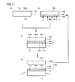
- Reference invention I is a method for producing a group III nitride composite substrate according to the above aspect, according to still another aspect, wherein the diameter of the substrate is bonded to the support substrate and the group III nitride film donor substrate.
- a method for manufacturing a group III nitride composite substrate A method for manufacturing a group III nitride composite substrate.
- Reference invention I is a method for producing a group III nitride composite substrate according to the above aspect, according to still another aspect, wherein the diameter of the substrate is bonded to the support substrate and the group III nitride film donor substrate.
- a method for manufacturing a group III nitride composite substrate is a method for producing a group III nitride composite substrate according to the above aspect, according to still another aspect, wherein the diameter of the substrate is bonded to the support substrate and the group III nitride film donor substrate.
- a method of manufacturing a group III nitride semiconductor device includes a step of further bonding a device support substrate on the group III nitride layer, and a step of removing the support substrate from the group III nitride composite substrate. , May further be included.
- Group III nitride composite substrate Referring to FIG. 6, group III nitride composite substrate 1, which is a reference form of reference invention I, is bonded to support substrate 11 and group III nitride film 13 having a thickness of 10 ⁇ m to 250 ⁇ m.
- the ratio s t / m t of the standard deviation s t of the thickness to the average value m t of the thickness of the III nitride film 13 is 0.001 or more is 0.2 or less
- III group ratio s o of the standard deviation s o of the absolute value of the off-angle with respect to the average value m o of the absolute value of the off-angle with respect to a predetermined plane surface of the orientation of the principal surface 13m nitride film 13 / Mo is 0.005 or more and 0.6 or less.
- the group III nitride composite substrate 1 of this reference embodiment has a diameter of 75 mm or more, and the group III nitride film 13 bonded on the support substrate 11 has a thickness of 10 ⁇ m or more and 250 ⁇ m or less. average 0.2 below the ratio s t / m t of the standard deviation s t a thickness of 0.001 or more with respect to m t of the average of the absolute value of the off angle relative to the plane of the predetermined plane orientation of the main surface 13m by the ratio s o / m o of the standard deviation s o of the absolute value of the off angle with respect to the value m o is 0.005 to 0.6, on the III nitride film 13, the crystal quality in large diameter Since at least one high group III nitride layer can be grown, a group III nitride semiconductor device having high characteristics can be obtained with high yield.
- the bonding form of the support substrate 11 and the group III nitride film 13 is not particularly limited, but in order to increase the bonding strength by bonding, the bonding film 12 is formed. It is preferable to interpose.
- the diameter of the group III nitride composite substrate 1 is 75 mm or more, preferably 100 mm or more, more preferably 125 mm or more, and more preferably 150 mm or more from the viewpoint of increasing the number of chips of a semiconductor device from one composite substrate. preferable. Further, the diameter of the group III nitride composite substrate 1 is preferably 300 mm or less, and more preferably 200 mm or less, from the viewpoint of reducing the warpage of the composite substrate and increasing the yield of the semiconductor device.
- the warp of the group III nitride composite substrate 1 on the group III nitride film 13 side is preferably 50 ⁇ m or less, more preferably 30 ⁇ m or less, and even more preferably 20 ⁇ m or less from the viewpoint of increasing the yield of the semiconductor device to be formed.
- the warp of the group III nitride composite substrate 1 on the group III nitride film 13 side is the least square that minimizes the square of the distance to any point in the main surface 13 m of the group III nitride film 13.
- the TTV (referred to as Total Tickness Variation, which is one of the evaluation indices of flatness, also referred to as GBIR (Global Backside Ideal Range)) of the group III nitride composite substrate 1 is a viewpoint of increasing the yield of the semiconductor device to be formed. Therefore, 30 ⁇ m or less is preferable, 20 ⁇ m or less is more preferable, and 10 ⁇ m or less is more preferable.
- the TTV of the group III nitride composite substrate 1 is the group III nitride composite substrate 1 measured in the thickness direction with the main surface of the support substrate 11 which is the back surface of the group III nitride composite substrate 1 as a reference plane.
- the level difference of the main surface of the group III nitride film 13 which is the surface of the group III nitride composite substrate 1 in a state where the surface is flattened using the surface as a reference surface is the flatness of the optical interference type. It is measured by a measuring device, a laser displacement meter, or the like.
- the ratio ⁇ III-N / ⁇ S of the thermal expansion coefficient ⁇ III-N of the group III nitride film to the thermal expansion coefficient ⁇ S of the support substrate is determined on the group III nitride composite substrate 1 and its group III nitride film 13. From the viewpoint of reducing warpage and cracking of the group III nitride layer to be grown, 0.75 or more and 1.25 or less are preferable, 0.8 or more and 1.2 or less are more preferable, and 0.9 or more and 1.1 or less are further included. 0.95 or more and 1.05 or less are particularly preferable.
- the ratio t III-N / t S of the thickness t III-N of the group III nitride film to the thickness t S of the support substrate is determined on the group III nitride composite substrate 1 and the group III nitride film 13. From the viewpoint of reducing warpage and cracking of the group III nitride layer to be grown, 0.02 to 1 is preferable, 0.06 to 0.7 is more preferable, 0.15 to 0.5 is more preferable, 0.2 or more and 0.4 or less are particularly preferable.
- the support substrate 11 is not particularly limited as long as it can support the group III nitride film 13, but from the viewpoint of reducing the cost by reducing the amount of expensive group III nitride used, A different composition substrate having a different composition is preferable. Furthermore, as described above, the ratio ⁇ III-N / ⁇ S of the thermal expansion coefficient ⁇ III-N of the group III nitride film 13 to the thermal expansion coefficient ⁇ S of the support substrate 11 is 0.75 or more and 1.25 or less.
- the support substrate 11 is made of mullite (3Al 2 O 3 .2SiO 2 to 2Al 2 O 3 .SiO 2 ), mullite-YSZ (yttria stabilized zirconia), spinel (MgAl 2 O 4 ), Al A sintered body of 2 O 3 —SiO 2 composite oxide, and a substrate formed of a sintered body obtained by adding an oxide, carbonate or the like to these, a molybdenum (Mo) substrate, a tungsten (W) substrate, or the like is preferable. .
- the elements contained in the oxide and carbonate are Ca, Mg, Sr, Ba, Al, Sc, Y, Ce, Pr, Si, Ti, Zr, V, Nb, Ta, Cr, Mn, Fe, Preferred examples include Co, Ni, Cu, and Zn.
- the root mean square roughness (hereinafter also referred to as RMS) of main surface 11n of support substrate 11 in group III nitride composite substrate 1 grows on group III nitride film 13 of group III nitride composite substrate 1. From the viewpoint of improving the crystal quality of the group III nitride layer to be formed, 12 nm or less is preferable, 6 nm or less is more preferable, and 2 nm or less is more preferable.
- the RMS of the main surface 11n of the support substrate 11 is polished before the group III nitride film 13 is bonded, or the main surface that is not bonded is polished after the group III nitride film 13 is bonded. Can be adjusted.
- the RMS of the main surface 11n of the support substrate 11 calculates the reference plane from each point of the main surface 11n of the support substrate 11, and is the value of the average positive square root of the square of the distance to each point from the reference plane. It is measured with an AFM (Atomic Force Microscope), an optical interference type roughness meter, a stylus type roughness meter, or the like.
- AFM Acoustic Force Microscope
- the main surface 11n of the support substrate 11 preferably has an RMS average value m S of 0.3 nm to 10 nm and a RMS standard deviation s S of 3 nm or less.
- the RMS average value m S is set to 10 nm or less
- the RMS standard deviation s S is set to 3 nm or less. Since a high-quality group III nitride layer can be grown, a semiconductor device can be obtained with a high yield.
- advanced surface polishing is required, and the cost is greatly increased.
- the RMS average value m S of the main surface 11n of the support substrate 11 is more preferably 0.3 nm or more and 5 nm or less, and further preferably 0.3 nm or more and 2 nm or less. Further, the RMS standard deviation s S of the main surface 11n of the support substrate 11 is more preferably 2 nm or less, and further preferably 1 nm or less.
- the RMS average value m S and the standard deviation s S of the main surface 11n of the support substrate 11 are respectively calculated from the RMS measured at 13 measurement points on the main surface 11n of the support substrate 11 shown in FIG. Mean value and standard deviation.
- the 13 measurement points P on the main surface 11n of the support substrate 11 shown in FIG. 7 are one center point P C and 4 perpendicular to the center point P C regardless of the diameter of the support substrate 11. and four outer points P O in the direction on a and the outer edge to 5mm inside each other's middle four points and four outer points located in the middle of one of the center points P C and four outer points P O It is composed of eight intermediate points P M that are a combination of four positions.
- the standard deviation here means the positive square root of unbiased variance.
- Bonding film 12 is not particularly limited as long as it can bond the support substrate 11 and the III nitride film 13, is a high viewpoint bonding strength between the supporting substrate 11 and the III nitride film 13, SiO 2 A film, a Si 3 N 4 film, a TiO 2 film, a Ga 2 O 3 film, or the like is preferable.
- III-nitride film 13 is a film formed of a group III nitride, GaN film, In x Al y Ga 1- xy N film (0 ⁇ x, 0 ⁇ y , x + y ⁇ 1) such as AlN film Etc.
- the thickness of the group III nitride film 13 is 10 ⁇ m or more, preferably 30 ⁇ m or more, more preferably 50 ⁇ m or more, and further preferably 100 ⁇ m or more from the viewpoint of forming a high-performance group III nitride semiconductor device. Further, the thickness of the group III nitride film 13 is 250 ⁇ m or less, preferably 200 ⁇ m or less, preferably 170 ⁇ m or less, and more preferably 150 ⁇ m or less, from the viewpoint of reducing the amount of expensive group III nitride used.
- the ratio s t / m t of the standard deviation s t thickness average thickness for the m t of the III nitride film 13 is 0.001 to 0.2, 0.001 to 0.15 Is preferable, 0.002 or more and 0.1 or less are more preferable, and 0.01 or more and 0.05 or less are more preferable.
- the ratio s t / m t since the cutting and polishing to control the highly thickness is required, costs increase.
- the ratio s t / m t is larger than 0.2, since the uniformity of the film thickness is reduced, the characteristics of the resulting semiconductor device is reduced.
- the ratio s o / m o occurs in larger when group III nitride film 13 portion morphology of group III nitride layer is lowered onto the plane than 0.6, also in-plane distribution of the impurity incorporation increases Therefore, the yield of the obtained semiconductor device is reduced.
- the crystal structure of the group III nitride film 13 is preferably a wurtzite structure from the viewpoint of obtaining a semiconductor device with good characteristics.
- the above-mentioned predetermined plane orientation that is most approximate to the main surface 13m of the group III nitride film 13 is not limited as long as it is suitable for a desired semiconductor device, and is ⁇ 0001 ⁇ , ⁇ 10-10 ⁇ , ⁇ 11- 20 ⁇ , ⁇ 21-30 ⁇ , ⁇ 20-21 ⁇ , ⁇ 10-11 ⁇ , ⁇ 11-22 ⁇ , ⁇ 22-43 ⁇ , and plane orientations off at 15 ° or less from their respective plane orientations Good.
- the surface orientation of the back surface of each of these surface orientations and the surface orientation turned off at 15 ° or less from the surface orientation of the back surface may be used. That is, the main surface 13m of the group III nitride film 13 may be any of a polar surface, a nonpolar surface, and a semipolar surface. Further, the principal surface 13m of the group III nitride film 13 is preferably a ⁇ 0001 ⁇ surface and its back surface from the viewpoint of easily increasing the diameter, and a ⁇ 10-10 ⁇ surface from the viewpoint of suppressing the blue shift of the resulting light emitting device. , ⁇ 20-21 ⁇ surfaces and their back surfaces are preferred.
- the standard deviation s o Group III average thickness value m t of the nitride film 13 are the standard deviation m t of thickness, the average value m o of the off-angles, and the off angles, respectively, shown in FIG. 7 These are the average value and standard deviation calculated from the thicknesses and off-angles measured at 13 measurement points on the main surface 13m of group III nitride film 13. Measurement point P of 13 points on the major surface 13m of the III nitride film 13 shown in FIG.
- the center point P C Four outer points P O on four directions perpendicular to each other and 5 mm inside from the outer edge, four points located between one center point P C and four outer points P O and four outer points And eight intermediate points P M obtained by combining four points located in the middle of each other.
- the standard deviation here means the positive square root of unbiased variance.
- the impurity metal atoms on the main surface 13m of the group III nitride film 13 are 3 ⁇ 10 12 atoms / cm 2 or less is preferable, 4 ⁇ 10 11 atoms / cm 2 or less is more preferable, and 1 ⁇ 10 11 atoms / cm 2 or less is more preferable.
- other impurities on the surface of the group III nitride film 13 can improve the crystal quality of the group III nitride layer grown on the group III nitride film 13 and improve the characteristics of the semiconductor device to be formed.
- the atoms are preferably 2 ⁇ 10 14 atoms / cm 2 or less, and the Si atoms are preferably 9 ⁇ 10 13 atoms / cm 2 or less.
- the RMS of the main surface 13m of the group III nitride film 13 is preferably 3 nm or less, more preferably 2 nm or less, from the viewpoint of improving the crystal quality of the group III nitride layer grown on the group III nitride film 13, and more preferably 1 nm. The following is more preferable.
- the main surface 13m of the group III nitride film 13 preferably has an RMS average value m III-N of 0.1 nm to 2 nm and an RMS standard deviation s III-N of 0.4 nm or less.
- the average value m III-N of the RMS is set to 2 nm or less
- the standard deviation s III-N of the RMS is set to 0.4 nm or less. Since a group III nitride layer having high crystal quality can be grown on the entire surface of 13 main surfaces 13m, a semiconductor device can be obtained with a high yield.
- the average RMS value m III-N of the main surface 13m of the group III nitride film 13 is more preferably 0.1 nm or more and 1.5 nm or less, and further preferably 0.2 nm or more and 1 nm or less. Further, the RMS standard deviation s III-N of the main surface 13m of the group III nitride film 13 is more preferably 0.3 nm or less, and further preferably 0.2 nm or less.
- the average value m III-N and standard deviation s III-N of the main surface 13m of the group III nitride film 13 are 13 points on the main surface of the group III nitride film 13 shown in FIG.
- the average value and the standard deviation calculated from the RMS measured at the measurement points are as described above.
- the group III nitride film 13 preferably has a dislocation density of 1 ⁇ 10 8 cm ⁇ 2 or less and a carrier concentration of 1 ⁇ 10 17 cm ⁇ 3 or more.
- a laminated group III nitride composite substrate 2 which is another reference form of reference invention I includes a group III nitride composite substrate 1 of reference form I-1 and a group III nitride composite substrate 1. And at least one group III nitride layer 20 disposed on group III nitride film 13.
- the laminated group III nitride composite substrate 2 of the present embodiment also has a group III nitride layer 20 arranged by growing on the group III nitride film 13 having a high crystal quality and a small thickness distribution and off-angle distribution. Since the crystal quality is high, a high-performance semiconductor device can be manufactured with high yield.
- the group III nitride layer 20 disposed on the group III nitride film 13 differs depending on the type of semiconductor device to be fabricated.
- group III nitride layer 20 has, for example, n-GaN layer 21, n-In 0.05 Ga 0.95 N layer 22, and a multiple quantum well structure.
- the active layer 23, the p-Al 0.09 Ga 0.91 N layer 24, and the p-GaN layer 25 can be used. Referring to FIG.
- the group III nitride layer includes, for example, a GaN layer 26 and an Al 0.2 Ga 0.8 N layer. 27.
- the group III nitride layer includes, for example, an n + -GaN layer 28 (with a carrier concentration of For example, 2 ⁇ 10 18 cm ⁇ 3 ) and an n ⁇ -GaN layer 29 (carrier concentration is 5 ⁇ 10 15 cm ⁇ 3 ), for example.
- group III nitride semiconductor device 4 which is still another reference form of reference invention I includes group III nitride film 13 in the group III nitride composite substrate of reference form 1, And at least one group III nitride layer 20 disposed on group III nitride film 13.
- the group III nitride semiconductor device 4 of the present embodiment has a group III nitride film 13 having a high crystal quality and a small thickness distribution and small off-angle distribution, and a group III having a high crystal quality arranged by growing on the group III nitride film 13. Since it includes the group nitride layer 20, it has high characteristics.
- the group III nitride layer 20 of the group III nitride semiconductor device 4 differs depending on the type of the group III nitride semiconductor device 4.
- group III nitride layer 20 includes, for example, n-GaN layer 21, n-In 0.05 Ga 0.95 N layer 22, multiple quantum wells.
- the active layer 23 having the structure, the p-Al 0.09 Ga 0.91 N layer 24, and the p-GaN layer 25 can be used. Referring to FIG.
- group III nitride semiconductor device 4 when the group III nitride semiconductor device 4 is an HEMT which is an example of an electronic device, the group III nitride layer 20 includes, for example, a GaN layer 26 and an Al 0.2 Ga 0.8 N layer 27. can do.
- group III nitride layer when fabricating an SBD which is another example of an electronic device as a semiconductor device, group III nitride layer is, for example, n + -GaN layer 28 (carrier concentration is 2 ⁇ 10 18 cm, for example). -3 ), n ⁇ -GaN layer 29 (carrier concentration is, for example, 5 ⁇ 10 15 cm ⁇ 3 ).
- the group III nitride semiconductor device 4 preferably further includes at least one of a support substrate 11 and a device support substrate 40 for supporting the group III nitride layer 20.
- the shape of the device support substrate 40 is not limited to a flat plate shape, and the group III nitride semiconductor device 4 can be formed by supporting the group III nitride film 13 and the group III nitride layer 20. As long as it can take any shape.
- Reference Form I-4 Method for Producing Group III Nitride Composite Substrate
- the manufacturing method of the group III nitride composite substrate which is still another reference form of Reference Invention I is the manufacturing method of Group III nitride composite substrate 1 of Reference Form I-1.
- the bonding substrate 1L, 1LS having a diameter of 75 mm or more is formed by bonding the support substrate 11 and the group III nitride film donor substrate 13D (FIGS. 12A to 12C, FIG. 13).
- the group III nitride composite substrate 1 having a group III nitride film having a low cost, a large diameter, a large film thickness and a high crystal quality is efficiently produced. be able to.
- the group III nitride film donor substrate 13D is positioned at a predetermined distance from the bonding main surface of the group III nitride film donor substrate 13D when cutting the group III nitride film donor substrate 13D.
- the predetermined distance on the surface to be processed is determined according to the thickness of the group III nitride film 13 of the group III nitride composite substrate 1 to be manufactured.
- the group III nitride film donor substrate 13D is cut to form the group III nitride film 13, and then the bonded main surface 13n of the group III nitride film 13 is formed.
- the thickness of group III nitride film 13 can be reduced by performing at least one of grinding, polishing, and etching from main surface 13m on the opposite side.
- the III of the group III nitride composite substrate 1 obtained by cutting is obtained.
- the main surface of group nitride film 13 is preferably polished.
- the polishing method is preferably precise polishing by CMP (chemical mechanical polishing), chemical polishing, or the like.
- the predetermined distance on the surface located at a predetermined distance from the bonded main surface 13n of the group III nitride film donor substrate 13D when the group III nitride film donor substrate 13D is cut is determined as follows. It is preferable to set the distance obtained by adding the thickness of the group III nitride film 13 of the target group III nitride composite substrate 1 to the thickness of the polishing allowance.
- the group III nitriding is performed on the surface located at a predetermined distance from the bonded main surface 13n of the group III nitride film donor substrate 13D of the bonding substrates 1L and 1LS.
- the material film donor substrate 13D is cut to form a group III nitride film 13.
- at least one of grinding, polishing and etching from the main surface 13m opposite to the bonded main surface 13n of the group III nitride film 13 is performed.
- the group III nitride composite substrate 1 including the group III nitride film 13 having a desired thickness of 10 ⁇ m or more and 250 ⁇ m or less is obtained by adjusting the film thickness to be reduced.
- the group III nitride film donor substrate is cut in the step of forming the group III nitride composite substrate, so that workability and efficiency in manufacturing are reduced.
- the thickness of the group III nitride film donor substrate 13D used is preferably greater than 500 ⁇ m, more preferably 1 mm or more, and even more preferably 2 mm or more.
- bonding film 12a is formed on main surface 11m of support substrate 11.
- the sub-process (FIGS. 12A and 13A) and the sub-process for forming the bonding film 12b on the main surface 13n of the group III nitride film donor substrate 13D (FIGS. 12B and 13B) ))
- a sub-process for bonding the bonding film 12a formed on the support substrate 11 and the bonding film 12b formed on the group III nitride film donor substrate 13D (FIGS. 12C and 13C) ,including.
- bonding film 12a is integrated and bonded to bonding film 12b described later.
- the film 12 is formed, and is formed of the same material as that of the bonding film 12.
- the method for forming the bonding film 12a is not particularly limited as long as it is suitable for the formation of the bonding film 12a.
- sputtering, CVD (chemical vapor) Phase deposition) method, PLD (pulse laser deposition) method, MBE (molecular beam growth) method, electron beam evaporation method and the like are preferable.
- CVD is particularly preferable because it increases the quality of the bonding film and increases the deposition rate.
- a P-CVD (plasma-chemical vapor deposition) method, a PE-CVD (plasma-assisted chemical vapor deposition) method, and the like are more preferable from the viewpoint that a film can be formed at a low temperature and a film forming speed is high.
- the LP-CVD (reduced pressure-chemical vapor deposition) method and the like are more preferable.
- annealing can be performed after the bonding films 12a and 12b are formed and before bonding. By this annealing, the bonding films 12a and 12b can be degassed to densify the bonding films 12a and 12b.
- the bonding film 12a is polished from the main surface 12am to a mirror surface (for example, a mirror surface having an RMS of 0.3 nm or less) from the viewpoint of increasing the bonding strength between the support substrate 11 and the group III nitride film donor substrate 13D.
- the method for polishing the main surface 12am of the bonding film 12a is not particularly limited, and for example, CMP (Chemical Mechanical Polishing) or the like is used. From the viewpoint of increasing the bonding strength, abrasive-free polishing with a liquid that does not contain abrasive grains can be performed after CMP in order to improve the cleanliness of the bonding film.
- non-abrasive polishing with an alkali such as KOH or TMAH (tetramethylammonium hydroxide), or an acid such as HCl, HNO 3 , or H 2 SO 4 can be performed.
- an alkali such as KOH or TMAH (tetramethylammonium hydroxide), or an acid such as HCl, HNO 3 , or H 2 SO 4
- scrub cleaning using a sponge, a brush, or the like can be performed in order to improve the cleanliness of the bonding film.
- Two-fluid cleaning, megasonic cleaning, ultrasonic cleaning, and the like can also be suitably performed.
- group III nitride film donor substrate 13D is This is a donor substrate that provides the group III nitride film 13 by separation in a post-subprocess.
- the method for preparing such a group III nitride film donor substrate 13D is not particularly limited, but from the viewpoint of obtaining a group III nitride film donor substrate 13D with good crystallinity, the HVPE (hydride vapor phase epitaxy) method, MOVPE (organic)
- a vapor phase method such as a metal vapor phase growth method, an MBE (molecular beam growth) method, a sublimation method, a liquid phase method such as a flux method, a high nitrogen pressure solution method, and an ammonothermal method is preferable.
- the group III nitride film donor substrate 13D prepared in this way is not particularly limited, but from the viewpoint of providing the group III nitride film 13 with good crystallinity, the crystal of the same degree as the group III nitride film 13 to be provided Specifically, the absolute angle of the off angle with respect to the average value m o of the absolute value of the off angle with respect to the plane of the predetermined plane orientation of the main surface 13m of the group III nitride film donor substrate 13D is preferable. it preferably has a specific s o / m o of the standard deviation s o value is 0.005 to 0.6.
- the material and method for forming the bonding film 12b and the polishing of the main surface 12bn are the same as the material and method for forming the bonding film 12a and the polishing of the main surface 12am, respectively.
- the bonding method is not particularly limited, and the bonding surface is cleaned and bonded as it is, then the direct bonding method in which the temperature is raised to about 600 ° C. to 1200 ° C. and the bonding surface is cleaned, and plasma or ions are used for cleaning.
- Surface activated bonding method in which bonding is performed in a low temperature atmosphere of about room temperature (for example, 25 ° C.) to about 400 ° C.
- the bonding strength can be further increased by raising the temperature to about 600 ° C. to 1200 ° C. after the bonding.
- the effect of increasing the bonding strength by raising the temperature to about 600 ° C. to 1200 ° C. after the bonding is large.
- the bonding film 12a and the bonding film 12b are integrated by bonding to form the bonding film 12, and the support substrate 11 and the group III nitride film donor substrate 13D are bonded with the bonding film 12 interposed therebetween.
- the bonded substrates 1L and 1LS are formed.
- the bonding strength can be increased by activating the bonding surfaces of the bonding films 12a and 12b before bonding.
- the activation of the bonding surface is not particularly limited, but is preferably performed by plasma treatment, ion treatment, chemical treatment with a chemical solution, cleaning treatment, CMP treatment or the like from the viewpoint of high activation effect.
- Group III nitride composite substrate formation process Referring to FIGS. 12D and 13D, in the step of forming group III nitride composite substrate 1, from bonding main surface 13n of group III nitride film donor substrate 13D of bonding substrates 1L and 1LS.
- the group III nitride composite substrate 1 is formed in which the support substrate 11 and the group III nitride film 13 are bonded together with the bonding film 12 interposed therebetween.
- the method for cutting the group III nitride film donor substrate 13D is not particularly limited, and examples thereof include a wire saw, a blade saw, laser processing, electric discharge processing, and water jet.
- the group III nitride film donor substrate 13D is cut with a wire saw
- the loose abrasive method is preferred.
- the wire tension is increased in order to reduce the bending of the wire due to the cutting resistance and increase the accuracy and flatness of the thickness. It is preferable to increase the speed.
- a highly rigid wire saw device is preferable.
- the wire is oscillated and the group III nitride film donor substrate 13D is oscillated in synchronization therewith.
- the group III nitride film donor substrate 13D moves in the cutting progress direction.
- the group III nitride film donor substrate 13D moves in a direction opposite to the cutting progress direction when the wire saw is positioned at an angle far from the perpendicular to the cutting progress direction of the group III nitride film donor substrate 13D.
- group III nitrides such as GaN are more brittle and easier to break than sapphire and SiC, and therefore cannot be cut well by the same cutting method as sapphire and SiC.
- the viscosity ⁇ (Pa ⁇ s) of the machining fluid for slicing, the flow rate Q (m 3 / s) of the machining fluid, and the wire linear velocity V (m / S), maximum cutting length L (m), cutting speed P (m / s), and simultaneous cutting number n expressed as ( ⁇ ⁇ Q ⁇ V) / (L ⁇ P ⁇ n).
- the resistance coefficient R (N) is in an appropriate range, specifically 4000 or more and 5000 or less.
- the group III nitride composite substrate 1 obtained by cutting has its desired thickness and off-angle and uniformity thereof polished by polishing the group III nitride film 13 and the main surfaces 13m and 11n of the support substrate 11.
- the fixation of the group III nitride composite substrate 1 to the polishing apparatus at the time of polishing can be performed by adsorption fixation or fixation by a back pad.
- the group III nitride composite substrate 1 may be attached to the holding plate and then attached to the polishing apparatus.
- mechanical pressurization such as vacuum chuck, air bag pressurization, weight, etc.
- the group III nitride composite substrate 1 can also be adsorbed and fixed. By uniformly attaching the group III nitride composite substrate 1 to the polishing apparatus, the thickness distribution and the off-angle distribution after polishing can be reduced.
- the thickness distribution and the off-angle distribution of the group III nitride film 13 of the group III nitride composite substrate 1 are reduced and the group III nitridation is performed.
- the main surface of the group III nitride film 13 of the group III nitride composite substrate 1 obtained by cutting from the viewpoint of removing the damaged layer due to the cutting of the material film 13 to maintain high crystal quality and smoothing the main surface. It is preferable to polish 13 m.
- the main bonding of the group III nitride film donor substrate 13D which is a surface for cutting the group III nitride film donor substrate 13D of the bonding substrates 1L and 1LS is performed.
- the predetermined distance on the surface located at a predetermined distance from the surface 13n is the thickness of the group III nitride film 13 of the group III nitride composite substrate 1 to be manufactured and the thickness of the polishing allowance. It is preferable that the distance is added.
- the polishing allowance is not particularly limited, but is preferably 10 ⁇ m or more, more preferably 20 ⁇ m or more, and even more preferably 30 ⁇ m or more from the viewpoint of reducing the thickness distribution and off-angle distribution and removing the damaged layer.
- the polishing allowance is preferably 100 ⁇ m or less, more preferably 80 ⁇ m or less, and even more preferably 60 ⁇ m or less, from the viewpoint of reducing material loss of the group III nitride film donor substrate 13D.
- the remaining group III nitride film donor substrate 13Dr is repeatedly used by polishing its main surface. Can do.
- a group III nitride film donor substrate 5D with a support in which a group III nitride film donor substrate support 15 is bonded to a group III nitride film donor substrate 13D is used.
- the group III nitride composite substrate 1 can be manufactured in the same manner as described above.
- the group III nitride film donor substrate 5D with the support since the group III nitride film donor substrate 13D is supported by the group III nitride film donor substrate support 15, the group III nitride film donor substrate 13D cannot stand alone. Even if it becomes as thin as possible, it can be used repeatedly.
- the bonding form of the group III nitride film donor substrate support 15 and the group III nitride film donor substrate 13D is not particularly limited, but the bonding strength by bonding is not limited. In order to increase the thickness, it is preferable to interpose the bonding film 14. Further, the group III nitride film donor substrate support 15 is not particularly limited, but is formed of a material having the same physical properties as the support substrate 11 from the viewpoint of high support strength and prevention of cracking and warping. It is preferable.
- the bonding film 14 is not particularly limited, but from the viewpoint of high bondability between the group III nitride film donor substrate support 15 and the group III nitride film donor substrate 13D, the SiO 2 film, the Si 3 N 4 film, the TiO 2 Two films, a Ga 2 O 3 film, and the like are preferable.
- the method for producing a group III nitride composite substrate of still another reference form of Reference Invention I is a method of producing Group III nitride composite substrate 1 of Reference Form I-1, A step of forming a bonded substrate 1L having a diameter of 75 mm or more by bonding the substrate 11 and the group III nitride film donor substrate 13D (FIGS.
- the group III nitride composite substrate 1 having a group III nitride film having a low cost, a large diameter, a large film thickness and a high crystal quality is efficiently produced. be able to.
- the manufacturing method of the group III nitride composite substrate 1 of the present embodiment at least one of grinding, polishing, and etching is performed from the main surface opposite to the bonded main surface of the group III nitride film donor substrate 13D.
- the group III nitride composite substrate 1 including the group III nitride film 13 having a desired thickness of 10 ⁇ m or more and 250 ⁇ m or less is obtained by adjusting the film thickness to be reduced.
- the manufacturing method of the group III nitride composite substrate 1 of this reference form it grinds from the main surface on the opposite side to the bonding main surface of the group III nitride film donor substrate in the step of forming the group III nitride composite substrate.
- the thickness of the group III nitride film donor substrate 13D used is preferably 500 ⁇ m or less, and 400 ⁇ m. The following is more preferable.
- FIGS. 14A to 14C the process of forming bonded substrate 1L is performed on main surface 11m of support substrate 11 in the same manner as the method for manufacturing a group III nitride composite substrate of Reference Embodiment I-4.
- a sub-process (FIG. 14A) for forming the bonding film 12a on the substrate a sub-process (FIG. 14B) for forming the bonding film 12b on the main surface 13n of the group III nitride film donor substrate 13D, and a support.
- the sub-process for forming the bonding film 12a on the main surface 11m of the support substrate 11 shown in FIG. 14A forms the bonding film 12a on the main surface 11m of the support substrate 11 shown in FIG.
- the sub-process for forming the bonding film 12b on the main surface 13n of the group III nitride film donor substrate 13D shown in FIG. 14B is performed on the main surface 13n of the group III nitride film donor substrate 13D shown in FIG.
- Group III nitride composite substrate formation process Referring to FIG. 14D, in the step of forming group III nitride composite substrate 1, grinding is performed from main surface 13m opposite to bonding main surface 13n of group III nitride film donor substrate 13D of bonding substrate 1L. Then, by performing at least one of polishing and etching, a group III nitride film 13 having a reduced thickness is formed from the group III nitride film donor substrate 13D, and the support substrate 11, the group III nitride film 13, Group III nitride composite substrate 1 bonded together with bonding film 12 interposed therebetween is formed.
- the method for grinding the group III nitride film donor substrate 13D is not particularly limited, and examples thereof include grinding using a grindstone or abrasive grains.
- the method for polishing the group III nitride film donor substrate 13D is not particularly limited, and examples thereof include rough polishing such as mechanical polishing, precision polishing such as CMP, and chemical polishing.
- the method for etching the group III nitride film donor substrate 13D is not particularly limited, and examples include wet etching using a chemical solution and dry etching such as RIE (reactive ion etching).
- the group III nitride film 13 of the group III nitride composite substrate 1 obtained by at least one of grinding and etching. It is preferable to polish the main surface 13m. From the viewpoint of reducing the thickness distribution and off-angle distribution and removing the damaged layer, the thickness reduction amount due to at least one of grinding, polishing, and etching is preferably 10 ⁇ m or more, more preferably 20 ⁇ m or more, and 30 ⁇ m or more. Further preferred.
- the amount of reduction in thickness due to at least one of grinding, polishing and etching is preferably 100 ⁇ m or less, more preferably 80 ⁇ m or less, and more preferably 60 ⁇ m or less from the viewpoint of reducing the material loss of the group III nitride film donor substrate 13D. Further preferred.
- a Group III nitride semiconductor device manufacturing method which is still another reference form of Reference Invention I includes a step of preparing Group III nitride composite substrate 1 of Reference Form I-1, and a Group III A step of growing at least one group III nitride layer 20 on the group III nitride film 13 of the nitride composite substrate 1 (FIG. 15A).
- a group III nitride semiconductor device having high characteristics can be manufactured with a high yield.
- the method of manufacturing a group III nitride semiconductor device of the present embodiment can be performed by the following steps.
- Group III nitride layer growth process Referring to FIG. 15A, in the step of growing at least one group III nitride layer 20 on group III nitride film 13 of group III nitride composite substrate 1, group III nitride layer 20 is formed.
- a gas phase method such as MOVPE method, MBE method, HVPE method, sublimation method, or liquid phase method such as flux method is suitable.
- the MOVPE method is suitable.
- the configuration of group III nitride layer 20 differs depending on the type of group III nitride semiconductor device 4.
- the group III nitride layer 20 includes, for example, an n-GaN layer 21, an n-In 0.05 Ga 0.95 N layer 22, a multiple layer on the group III nitride film 13.
- An active layer 23 having a quantum well structure, a p-Al 0.09 Ga 0.91 N layer 24, and a p-GaN layer 25 can be grown in this order.
- the laminated group III nitride composite substrate 2 is obtained by growing at least one group III nitride layer 20 on the group III nitride film 13 of the group III nitride composite substrate 1. .
- the step of further bonding the device support substrate 40 on the group III nitride layer 20 includes forming the first electrode on the group III nitride layer 20 of the laminated group III nitride composite substrate 2. 30 and the pad electrode 33, the pad electrode 43 and the bonding metal film 44 are formed on the device support substrate 40, and the bonding metal film 44 is bonded to the pad electrode 33.
- the laminated substrate 3 is obtained by this process.
- a Si substrate, a CuW substrate, or the like is used for the device support substrate 40.
- the step of removing support substrate 11 from group III nitride composite substrate 1 is performed by removing support substrate 11 of group III nitride composite substrate 1 from laminated substrate 3. .
- the bonding film 12 can also be removed.
- a method for removing the support substrate 11 and the bonding film 12 is not particularly limited, and grinding, etching, and the like are preferably used.
- the support substrate 11 formed of a material that has low hardness, strength, and wear resistance and is easily cut can be removed by at least one of grinding and polishing from the viewpoint of reducing manufacturing costs.
- the support substrate 11 formed of a material that dissolves in a chemical solution such as acid or alkali can be removed by etching with a chemical solution from the viewpoint of low manufacturing cost.
- the support substrate 11 has a larger number of ceramics or the like than a support substrate formed of a single crystal material such as sapphire, SiC, or a group III nitride (for example, GaN).
- a support substrate made of a crystalline material is preferred.
- the second electrode 50 is formed on the group III nitride film 13 exposed by removing the support substrate 11 and the bonding film 12 from the laminated substrate 3, and the device support substrate 40 is formed.
- a device supporting substrate electrode 45 is formed on the substrate.
- Reference invention II reduces the manufacturing cost of a semiconductor device, enables the manufacture of a group III nitride semiconductor device with a high yield, has a low cost, a large diameter, a large group III nitride film, and a group III nitride.
- the present invention relates to a group III nitride composite substrate having a small temperature distribution on a main surface during growth of a physical layer and a manufacturing method thereof, a laminated group III nitride composite substrate, a group III nitride semiconductor device, and a manufacturing method thereof.
- Group III nitrides such as GaN are suitably used for semiconductor devices because they have excellent semiconductor properties.
- group III nitrides such as GaN have good material characteristics different from those of Si, GaAs, SiC, and the like in various types of semiconductor devices, for example, light emitting devices and electronic devices, and therefore can be used for various devices. it can.
- Japanese Patent Laid-Open No. 2009-126722 discloses a self-standing group III nitride substrate having a diameter of 25 mm or more and 160 mm or more and a thickness of 100 ⁇ m or more and 1000 ⁇ m or less as a semiconductor device substrate, as a specific example, a diameter of 100 mm and a thickness.
- a self-standing GaN substrate having a thickness of 400 ⁇ m is disclosed.
- Japanese Patent Application Laid-Open No. 2008-010766 discloses a heterogeneous substrate having a chemical composition different from that of GaN as a substrate for manufacturing a semiconductor device, and a GaN thin film having a thickness of 0.1 ⁇ m or more and 100 ⁇ m or less bonded to the heterogeneous substrate. And a GaN thin film bonded substrate having a diameter of 50.8 mm in which a sapphire substrate and a GaN thin film having a thickness of 0.1 ⁇ m or 100 ⁇ m are bonded. .
- Japanese Unexamined Patent Application Publication No. 2010-182936 discloses a composite substrate including a support substrate, a nitride semiconductor layer, and a bonding layer provided between the support substrate and the nitride semiconductor layer as a semiconductor device substrate.
- a composite substrate is disclosed in which the thickness of a GaN layer is 5 ⁇ m to 220 ⁇ m and the diameter is 50.8 mm.
- the GaN thin film bonded substrate disclosed in JP 2008-010766 A with a GaN thin film thickness of 0.1 ⁇ m is ion-implanted to form the GaN thin film.
- the thickness of the GaN thin film is preferably 10 ⁇ m or more.
- the thickness of the GaN thin film is increased, the depth of the ion implantation from the main surface is increased. There is a problem that the variation becomes large and the variation in the thickness of the GaN thin film of the obtained GaN thin film composite substrate becomes large.
- the GaN thin film composite substrate disclosed in Japanese Patent Application Laid-Open No. 2008-010766 and the composite substrate disclosed in Japanese Patent Application Laid-Open No. 2010-182936 are both bonded with a group III nitride film or layer on a support substrate.
- a group III nitride layer is grown on the substrate to manufacture a group III nitride semiconductor device.
- the temperature variation on the main surface of the substrate tends to increase, there is a problem that it is difficult to increase the yield of the manufactured semiconductor device when the diameter of the substrate is increased.
- Reference invention II solves the above-mentioned problems, reduces the cost of manufacturing a semiconductor device, enables the manufacture of a group III nitride semiconductor device with a high yield, and has a low cost and a large diameter group III nitride.
- Group III nitride composite substrate having a thick material film and a small temperature distribution (ie, variation, the same applies hereinafter) on the main surface during the growth of the group III nitride layer, a method for manufacturing the same, and a laminated group III nitride composite It is an object of the present invention to provide a substrate, a group III nitride semiconductor device, and a manufacturing method thereof.
- Reference Invention II is a Group III nitride composite substrate having a diameter of 75 mm or more in which a supporting substrate and a Group III nitride film having a thickness of 10 ⁇ m or more and 250 ⁇ m or less are bonded to each other.
- the average value m S of the root mean square roughness of the main surface on the substrate side is 0.3 nm or more and 20 nm or less, and the root mean square roughness of the mean value m S of the root mean square roughness of the main surface on the support substrate side is
- This is a group III nitride composite substrate in which the ratio s S / m S of the standard deviation s S is 0.005 or more and 0.4 or less.
- the average value m III-N of the root mean square roughness of the main surface on the group III nitride film side is set to 0.15 nm or more and 3 nm or less
- the group III nitride the ratio s III-N / m III- N of the standard deviation s III-N to the average value m III-N root mean square roughness of the main surface of the film side can be 0.008 to 0.5
- the ratio W / D of the warpage W of the main surface on the support substrate side to the diameter D can be set to ⁇ 7 ⁇ 10 ⁇ 4 or more and 8 ⁇ 10 ⁇ 4 or less.
- the ratio ⁇ III-N / ⁇ S of the thermal expansion coefficient of the III nitride film to the thermal expansion coefficient alpha S of the supporting substrate alpha III-N and 0.75 to 1.25, the thickness of the support substrate t the ratio t III-N / t S of thickness t III-N III nitride film to S may be 0.02 or more and 1 or less.
- the thermal conductivity lambda S of the supporting substrate may be a 3W ⁇ m -1 ⁇ K -1 or more 280W ⁇ m -1 ⁇ K -1 or less.
- the Young's modulus E S of the supporting substrate can be 150GPa than 500GPa or less.
- a diameter can be 100 mm or more.
- the diameter can be 125 mm or more and 300 mm or less.
- the reference invention II is a group III nitride composite substrate according to the above aspect, and at least one layer of III disposed on the main surface of the group III nitride composite substrate on the group III nitride film side And a group III nitride composite substrate including a group nitride layer.
- the group III nitride film in the group III nitride composite substrate according to the above aspect and at least one group III nitride disposed on the group III nitride film A III-nitride semiconductor device comprising a layer.
- Reference invention II is a method for producing a group III nitride composite substrate according to the above aspect, according to still another aspect, wherein the diameter is increased by laminating a support substrate and a group III nitride film donor substrate.
- the main surface on the support substrate side is polished by polishing the main surface on the support substrate side of the group III nitride composite substrate before, during or after the step of forming the group III nitride composite substrate and any one of the above steps. Adjusting the root mean square roughness of the surface.
- a method for producing a group III nitride composite substrate is a method for producing a group III nitride composite substrate.
- Reference invention II is a method for producing a group III nitride composite substrate according to the above aspect, according to still another aspect, wherein the diameter is increased by laminating a support substrate and a group III nitride film donor substrate.
- the square of the main surface on the support substrate side is polished by polishing the main surface on the support substrate side of the group III nitride composite substrate before, during or after any one of the above steps. Adjusting the average square root roughness, and a method for producing a group III nitride composite substrate.
- At least one layer is provided on the main surface of the group III nitride composite substrate on the group III nitride film side of the step of preparing the group III nitride composite substrate according to the above aspect. And a step of growing a group III nitride layer.
- the group III nitride semiconductor device manufacturing method according to this aspect of the reference invention II may further include a step of removing the support substrate from the group III nitride composite substrate after the step of growing the group III nitride layer. Furthermore, after the step of growing the group III nitride layer and before the step of removing the support substrate, a step of bonding the device support substrate onto the group III nitride layer can be further included.
- Reference Invention II the cost for manufacturing a semiconductor device is reduced, and a Group III nitride semiconductor device can be manufactured with a high yield, the cost is low, the diameter is large, the Group III nitride film is thick, and III Provided are a group III nitride composite substrate having a small temperature distribution on the main surface during the growth of the group nitride layer, a manufacturing method thereof, a laminated group III nitride composite substrate, a group III nitride semiconductor device, and a manufacturing method thereof can do.
- group III nitride composite substrate 1 which is a reference form of reference invention II, is bonded to support substrate 11 and group III nitride film 13 having a thickness of 10 ⁇ m to 250 ⁇ m.
- a group III nitride composite substrate 1 having a diameter of 75 mm or more, and an average value m S of root mean square roughness (hereinafter also referred to as RMS) of the main surface 11n on the support substrate 11 side is 0.3 nm or more and 20 nm or less.
- the ratio s S / m S of the RMS standard deviation s S to the RMS average value m S of the main surface 11n on the support substrate 11 side is 0.005 or more and 0.4 or less.
- the group III nitride composite substrate 1 of the present embodiment has a small temperature distribution (that is, variation) on the main surface during the growth of the group III nitride layer for manufacturing the group III nitride semiconductor device, A high-quality group III nitride layer can be grown, and thus a high-quality group III nitride semiconductor device can be manufactured with a high yield. This will be described in more detail below.
- group III nitride composite substrate 1 of the present embodiment has a structure in which group III nitride film 13 is bonded onto support substrate 11, and a group III nitride semiconductor.
- the main surface 11n on the side of the support substrate 11 corresponding to the back surface side of the group III nitride composite substrate 1 is arranged to face the main surface of a susceptor (not shown) provided with a temperature raising device.
- at least one group III nitride layer 20 is grown on the main surface 13m on the group III nitride film 13 side corresponding to the front surface side of the group III nitride composite substrate 1.
- the group III nitride composite substrate 1 of the present embodiment has a diameter of 75 mm or more, and the thickness of the group III nitride film 13 bonded on the support substrate 11 is 10 ⁇ m or more and 250 ⁇ m or less.
- the average RMS value m S of the main surface 11n on the side is 0.3 nm or more and 20 nm or less, and the ratio of the RMS standard deviation s S to the RMS average value m S of the main surface 11n on the support substrate 11 side s S / m S Is not less than 0.005 and not more than 0.4, and the average and distribution of RMS on the back surface side of the large-diameter group III nitride composite substrate 1 from the main surface of the heated susceptor is smaller on the support substrate 11 side.
- the entire large-diameter group III nitride composite substrate 1 Since heat is uniformly transmitted to the entire main surface 11n, the entire large-diameter group III nitride composite substrate 1 is uniformly heated. As a result, the temperature distribution on the main surface 13m on the group III nitride film 13 side, which is the surface side of the large-diameter group III nitride composite substrate 1, is small and uniform. Since the group III nitride layer 20 having a high crystal quality and a uniform large diameter can be grown on the main surface 13m on the group III nitride film 13 side of the substrate 1, a group III nitride semiconductor device having high characteristics can be manufactured. Can be manufactured well.
- the form in which the support substrate 11 and the group III nitride film 13 are bonded is not particularly limited, but in order to increase the bonding strength by bonding. It is preferable to interpose the bonding film 12.
- the thickness of group III nitride film 13 of group III nitride composite substrate 1 of the present embodiment is not less than 10 ⁇ m and not more than 250 ⁇ m.
- the thickness of the group III nitride film 13 means an average value calculated from the thicknesses measured at 13 measurement points on the main surface 13m of the group III nitride film 13 shown in FIG.
- the 13 measurement points P on the main surface of the group III nitride film 13 shown in FIG. 7 are based on one center point P C and its center point P C regardless of the diameter of the group III nitride film.
- the thickness of the group III nitride film 13 is required to be 10 ⁇ m or more, preferably 30 ⁇ m or more, more preferably 80 ⁇ m or more, further preferably 100 ⁇ m or more, from the viewpoint of growing a group III nitride layer having high crystal quality. From the viewpoint of suppressing the material cost of the group III nitride composite substrate 1, 250 ⁇ m or less is necessary, preferably 200 ⁇ m or less, more preferably 180 ⁇ m or less, and further preferably 130 ⁇ m or less.
- the group III nitride composite substrate 1 of the present embodiment has a diameter of 75 ⁇ m or more.
- the diameter of the group III nitride composite substrate 1 is required to be 75 mm or more, preferably 100 mm or more, more preferably 125 mm or more, and 150 mm or more from the viewpoint of increasing the number of chips of a semiconductor device from one composite substrate. Is more preferable.
- the diameter of the group III nitride composite substrate 1 is preferably 300 mm or less, and more preferably 200 mm or less, from the viewpoint of reducing the warpage of the composite substrate and increasing the yield of the semiconductor device.
- group III nitride composite substrate 1 of the present embodiment has an RMS average value m S of main surface 11n on the support substrate 11 side of 0.3 nm or more and 20 nm or less.
- the ratio s S / m S of the RMS standard deviation s S to the RMS average value m S of the 11-side main surface 11n is 0.005 or more and 0.4 or less.
- the main surface 11n on the support substrate 11 side which is the back side of the group III nitride composite substrate 1
- the average value m S of the RMS is required to be 20 nm or less, preferably 10 nm or less, more preferably 5 nm or less, and the standard deviation of the RMS with respect to the average value m S of the RMS the ratio s S / m S of s S, it is necessary to 0.4 or less, preferably 0.3 or less, more preferably 0.2 or less.
- the average value m S of the RMS is 0.3 nm.
- the above is necessary, preferably 0.5 nm or more, more preferably 1 nm or more, and the ratio s S / m S of the RMS standard deviation s S to the RMS average value m S must be 0.005 or more. Yes, 0.01 or more is preferable, and 0.05 or more is more preferable.
- the RMS average value m S and standard deviation s S of main surface 11 n of group III nitride composite substrate 1 on the support substrate 11 side are respectively on main surface 11 n of support substrate 11. These are the average value and standard deviation calculated from the RMS measured at 13 measurement points P.
- the 13 measurement points P on the main surface 11n of the support substrate 11 shown in FIG. 7 are one center point P C and 4 perpendicular to the center point P C regardless of the diameter of the support substrate 11.
- the standard deviation here means the positive square root of unbiased variance.
- the RMS measured at 13 measurement points P on the main surface 11n of the support substrate 11 shown in FIG. 7 is each point in the measurement area of 85 ⁇ m ⁇ 85 ⁇ m square centering on the measurement point P.
- the standard plane is calculated from the value, and the mean square value of the mean square of the distance to each point from the reference plane is used.
- AFM Anatomic Force Microscope
- optical interference roughness meter laser microscope
- stylus type Measured with a roughness meter is used.
- the RMS average value m S and standard deviation s S of the main surface 11n on the support substrate 11 side of the group III nitride composite substrate 1 are polished when the main surface 11n of the support substrate 11 is polished, as will be described later. It can be adjusted according to the physical properties of the agent, the surface plate and the polishing pad, the shape of the surface plate and the polishing pad, and the polishing conditions.
- the average RMS value m III-N of main surface 13m on the group III nitride film 13 side is 0.15 nm or more and 3 nm or less.
- the ratio s III-N / m III-N of the standard deviation s III-N to the RMS average value m III-N of the main surface 13m on the group III nitride film 13 side is 0.008 or more and 0.5 or less Is preferred.
- the average value of the RMS m III-N is preferably 3 nm or less, more preferably 2 nm or less, and even more preferably 1.6 nm or less, and the ratio of the RMS standard deviation s III-N to the RMS average value m III-N s III-N / M III-N is preferably 0.5 or less, more preferably 0.4 or less, and still more preferably 0.2 or less.
- the average value m III-N of the RMS is preferably at least 0.15 nm, more preferably at least 0.4 nm, more preferably at least 0.8 nm
- the ratio s III-N of the standard deviation s III-N of the RMS for the average value m III-N of the RMS / M III-N is preferably 0.008 or more, more preferably 0.02 or more, and even more preferably 0.05 or more.
- the RMS average value m III-N and the standard deviation s III-N of the main surface 13m on the group III nitride film 13 side of the group III nitride composite substrate 1 are III, respectively. These are an average value and a standard deviation calculated from RMS measured at 13 measurement points P on the main surface 13m of the group nitride film 13.
- the 13 measurement points P on the main surface 13m of the group III nitride film 13 shown in FIG. 7 are one center point P C and the center point P C regardless of the diameter of the group III nitride film 13.
- the RMS measured at 13 measurement points P on the main surface 13m of the group III nitride film 13 shown in FIG. 7 is within a measurement region of 85 ⁇ m ⁇ 85 ⁇ m square with the measurement point P as the center.
- the standard plane is calculated from each point, and the value of the positive square root of the mean square of the distance to each point from the reference plane is used.
- AFM Anatomic Force Microscope
- optical interference roughness meter laser microscope, Measured with a stylus roughness meter.
- the RMS average value m III-N and standard deviation s III-N of the main surface 13m on the group III nitride film 13 side of the group III nitride composite substrate 1 are the group III nitride film 13 as will be described later. It can be adjusted according to the physical properties of the abrasive, the surface plate and the polishing pad, the shape of the surface plate and the polishing pad, and the polishing conditions when polishing the main surface 13m.
- the ratio W / D of the warp W of the main surface 11n on the support substrate 11 side with respect to the diameter D is ⁇ 7 ⁇ 10 ⁇ 4 or more.
- ⁇ 10 ⁇ 4 or less is preferable, ⁇ 4 ⁇ 10 ⁇ 4 or more and 5 ⁇ 10 ⁇ 4 or less is more preferable, ⁇ 2.5 ⁇ 10 ⁇ 4 or more and 3 ⁇ 10 ⁇ 4 or less is more preferable, and ⁇ 1 ⁇ 10 ⁇ 4 More preferably, it is 1.5 ⁇ 10 ⁇ 4 or less.
- the sign of the warp W and the ratio W / D is a + (positive) sign when the main surface 11n on the support substrate 11 side is warped concavely, and the main surface on the support substrate 11 side warps convexly.
- the thing is a minus sign.
- the ratio W / D of the warp W of the main surface 11n on the support substrate 11 side to the diameter D of the group III nitride composite substrate 1 is preferably ⁇ 7 ⁇ 10 ⁇ 4 or more and 8 ⁇ 10 ⁇ 4 or less, more preferably ⁇ 4 ⁇ 10 ⁇ 4 or more and 5 ⁇ 10 ⁇ 4 or less, more preferably ⁇ 2.5 ⁇ 10 ⁇ 4 or more and 3 ⁇ 10 ⁇ 4 or less, and particularly preferably ⁇ 1 ⁇ 10 ⁇ 4 or more and 1.5 ⁇ 10 ⁇ 4 or less.
- the group III nitride layer is grown on the main surface 13m on the group III nitride film 13 side of the group III nitride composite substrate 1, the group III nitride having a large diameter from the main surface of the heated susceptor is grown. Since heat is uniformly transmitted to the entire main surface 11n on the support substrate 11 side of the compound composite substrate 1, the entire group III nitride composite substrate 1 is uniformly heated. As a result, the temperature on the main surface 13m on the group III nitride film 13 side which is the surface side of the group III nitride composite substrate 1 has a small distribution and becomes uniform. Since a group III nitride layer having a high crystal quality and a uniform large diameter can be grown on the main surface 13m on the material film 13 side, a group III nitride semiconductor device having high characteristics can be manufactured with a high yield.
- group III nitride composite substrate 1 of the present embodiment suppresses warping and cracking of group III nitride composite substrate 1 and group III nitride layer grown on group III nitride film 13.
- the ratio ⁇ III-N / ⁇ S of the thermal expansion coefficient ⁇ III-N of the group III nitride film 13 to the thermal expansion coefficient ⁇ S of the support substrate 11 is 0.75 or more and 1.25 or less are preferable, 0.85 or more and 1.15 or less are more preferable, and 0.95 or more and 1.05 or less are more preferable.
- the thermal expansion coefficient ⁇ S of the support substrate 11 and the thermal expansion coefficient ⁇ III-N of the group III nitride film 13 can be measured by a thermomechanical analyzer.
- group III nitride composite substrate 1 suppresses warping and cracking of group III nitride composite substrate 1 and group III nitride layer grown on group III nitride film 13.
- the ratio t III-N / t S of the thickness t III-N of the group III nitride film 13 to the thickness t S of the support substrate 11 is 0. 02 or more and 1 or less are preferable, 0.1 or more and 0.6 or less are more preferable, and 0.2 or more and 0.4 or less are more preferable.
- the thickness t S of the support substrate 11 and the thickness t III-N of the group III nitride film 13 can be measured by observing the cross section of the film with an optical microscope and / or SEM, a digital indicator, or the like.
- the support substrate with respect to the thickness t S of the thermal expansion coefficient alpha III-N ratio ⁇ III-N / ⁇ S 0.75 to 1.25 and the supporting substrate 11 of the group III nitride layer 13 on the thermal expansion coefficient alpha S 11
- the ratio t III-N / t S of the group III nitride film thickness t III-N is preferably 0.02 or more and 1 or less, and the ratio ⁇ III-N / ⁇ S is 0.85 or more and 1.15 or less.
- t III-N / t S is more preferably from 0.1 to 0.6, the ratio ⁇ III-N / ⁇ S is from 0.95 to 1.05 and the ratio t III-N / t S is 0.2. More preferably, it is 0.4 or less.
- the support substrate 11 included in the group III nitride composite substrate 1 of the present embodiment is not particularly limited as long as it can support the group III nitride film 13, but reduces the amount of expensive group III nitride used. From the viewpoint of reducing costs, it is preferable to use a different composition substrate having a chemical composition different from that of the group III nitride.
- the group III nitride composite substrate 1 of the present embodiment has the ratio ⁇ III-N / ⁇ of the thermal expansion coefficient ⁇ III-N of the group III nitride film 13 to the thermal expansion coefficient ⁇ S of the support substrate 11.
- S is preferably 0.75 or more and 1.25 or less.
- the thermal conductivity lambda S is preferably 3W ⁇ m -1 ⁇ K -1 or more 280W ⁇ m -1 ⁇ K -1 or less of the supporting substrate 11, 5W ⁇ m - 1 ⁇ K ⁇ 1 or more and 210 W ⁇ m ⁇ 1 ⁇ K ⁇ 1 or less is more preferable, and 10 W ⁇ m ⁇ 1 ⁇ K ⁇ 1 or more and 120 W ⁇ m ⁇ 1 ⁇ K ⁇ 1 or less is more preferable.
- the thermal conductivity ⁇ S of the support substrate 11 can be measured by a laser flash method.
- Support substrate having a thermal conductivity ⁇ S of preferably 3 W ⁇ m ⁇ 1 ⁇ K ⁇ 1 or more, more preferably 5 W ⁇ m ⁇ 1 ⁇ K ⁇ 1 or more, more preferably 10 W ⁇ m ⁇ 1 ⁇ K ⁇ 1 or more.
- the group III nitride composite substrate 1 having the main surface 13m of the group III nitride film 13 of the group III nitride composite substrate 1 efficiently generates heat from the main surface of the susceptor when the group III nitride layer is grown. Can tell.
- Thermal conductivity lambda S is preferably 280W ⁇ m -1 ⁇ K -1 or less, more preferably 210W ⁇ m -1 ⁇ K -1 or less, more preferably 120W ⁇ m -1 ⁇ K -1 or less, particularly preferably
- the group III nitride composite substrate 1 having the support substrate 11 of 50 W ⁇ m ⁇ 1 ⁇ K ⁇ 1 or less is a group III nitride composite substrate that generates heat from the main surface of the susceptor when the group III nitride layer is grown. 1 can be transmitted uniformly to the entire main surface of the group III nitride film 13.
- Thermal conductivity lambda S is 280W ⁇ m -1 ⁇ K -1 or less of the supporting substrate 11, than when the heat conductivity lambda S is used SiC substrate of approximately 300W ⁇ m -1 ⁇ K -1 as a supporting substrate,
- the group III nitride layer is grown, heat from the main surface of the susceptor can be uniformly transmitted to the entire main surface of the group III nitride film 13 of the group III nitride composite substrate 1.
- the Young's modulus E S is less preferred 500GPa than 150GPa of the support substrate 11 or less, more preferably more than 200 GPa 350 GPa.
- the Young's modulus E S of the supporting substrate 11 can be measured by a resonance method.
- Young's modulus E S is preferably 150GPa or more, more preferably Group III nitride composite substrate 1 having the above supporting substrate 11 200 GPa may form a group III nitride semiconductor devices by growing a Group III nitride layer thereon In doing so, it is possible to prevent the group III nitride composite substrate 1 and / or the group III nitride layer from warping.
- Young's modulus E S is preferably not more than 500GaPa, more preferably Group III nitride composite substrate 1 having the supporting substrate 11 350 GPa is formed a Group III nitride semiconductor devices by growing a Group III nitride layer thereon In doing so, it is possible to suppress the occurrence of cracks and / or cracks in the group III nitride composite substrate 1 and / or the group III nitride layer.
- the support substrate 11 is not particularly limited. From the above viewpoint, the ratio ⁇ III-N / ⁇ S of the thermal expansion coefficient ⁇ III-N of the group III nitride film 13 to the thermal expansion coefficient ⁇ S of the support substrate 11 is 0.75 to 1.25, the thermal conductivity lambda S is 3W ⁇ m -1 ⁇ K -1 or more 280W ⁇ m -1 ⁇ K -1 or less of the supporting substrate 11, and the Young's modulus E S of the supporting substrate 11 is Those satisfying at least one of 150 GPa or more and 500 GPa or less are preferable.
- mullite 3Al 2 O 3 .2SiO 2 to 2Al 2 O 3 .SiO 2
- mullite-YSZ yttria stabilized zirconia
- spinel MgAl 2 O 4
- a sintered body of Al 2 O 3 —SiO 2 composite oxide and a substrate formed of a sintered body obtained by adding an oxide, carbonate, etc., molybdenum (Mo) substrate, tungsten (W)
- Mo molybdenum
- W tungsten
- the elements contained in the oxide and carbonate are Ca, Mg, Sr, Ba, Al, Sc, Y, Ce, Pr, Si, Ti, Zr, V, Nb, Ta, Cr, Mn, Fe, Preferred examples include Co, Ni, Cu, and Zn.
- the support substrate 11 may contain any of single crystal, polycrystal, and non-crystal, it can be easily removed by grinding or etching at the time of device formation, and from the viewpoint of maintaining strength capable of suppressing warpage and cracking. It is preferable that a polycrystal is included.
- the bonding film 12 that can be included in the group III nitride composite substrate 1 of the present embodiment is not particularly limited as long as it can bond the support substrate 11 and the group III nitride film 13. From the viewpoint of high bondability between the support substrate 11 and the group III nitride film 13, a SiO 2 film, a Si 3 N 4 film, a TiO 2 film, a Ga 2 O 3 film, or the like is preferable.
- III-nitride layer 13 of this preferred embodiment is a film formed of a group III nitride, In x Al y Ga 1- xy N film (0, such as GaN film, AlN film ⁇ x, 0 ⁇ y, x + y ⁇ 1) and the like.
- the thickness of the group III nitride film 13 is required to be 10 ⁇ m or more, preferably 30 ⁇ m or more, more preferably 80 ⁇ m or more, and 100 ⁇ m. The above is more preferable. Further, as described above, the thickness of the group III nitride film 13 is 250 ⁇ m or less, preferably 200 ⁇ m or less, more preferably 180 ⁇ m or less, and more preferably 130 ⁇ m from the viewpoint of reducing the amount of expensive group III nitride used. The following is more preferable.
- the crystal structure of the group III nitride film 13 is preferably a wurtzite structure from the viewpoint of obtaining a semiconductor device with good characteristics.
- the above-mentioned predetermined plane orientation that is most approximate to the main surface of the group III nitride film 13 is not limited as long as it is suitable for a desired semiconductor device, and is ⁇ 0001 ⁇ , ⁇ 10-10 ⁇ , ⁇ 11-20 ⁇ , ⁇ 21-30 ⁇ , ⁇ 20-21 ⁇ , ⁇ 10-11 ⁇ , ⁇ 11-22 ⁇ , ⁇ 22-43 ⁇ , and their respective plane orientations were turned off at 15 ° or less (15 ° or less)
- the plane orientation may be shifted by an angle of Further, the surface orientation of the back surface of each of these surface orientations and the surface orientation turned off at 15 ° or less from the surface orientation of the back surface may be used.
- the main surface 13m of the group III nitride film 13 may be any of a polar surface, a nonpolar surface, and a semipolar surface.
- the principal surface 13m of the group III nitride film 13 is preferably a ⁇ 0001 ⁇ surface and its back surface from the viewpoint of easily increasing the diameter, and a ⁇ 10-10 ⁇ surface from the viewpoint of suppressing the blue shift of the resulting light emitting device. , ⁇ 20-21 ⁇ surfaces and their back surfaces are preferred.
- the impurity metal atoms in the main surface 13m of the group III nitride film 13 are 1 ⁇ 10 13 atoms / cm 2 or less is preferable, 3 ⁇ 10 12 atoms / cm 2 or less is more preferable, 1 ⁇ 10 12 atoms / cm 2 or less is more preferable, and 1 ⁇ 10 11 atoms / cm 2 or less is particularly preferable.
- Support substrate 11 includes mullite (3Al 2 O 3 .2SiO 2 to 2Al 2 O 3 .SiO 2 ), mullite-YSZ (yttria stabilized zirconia), spinel (MgAl 2 O 4 ), Al 2 O 3 —SiO 2 system.
- the group III nitride composite substrate 1 including a substrate such as a composite oxide sintered body is cleaned with suppressed elution of metal atoms from the support substrate 11, for example, scrub cleaning using a surfactant and / or pure water.
- Single-sided cleaning such as two-fluid cleaning or megasonic cleaning (cleaning using ultrasonic waves in the frequency range of 500 kHz to 5 MHz) and single-wafer cleaning using low concentrations of acid and / or alkali (this side is III
- This side is III
- the concentration of impurity metal atoms on the main surface 13m of the group III nitride film 13 is reduced by cleaning the main surface 13m of the group nitride film 13).
- a protective film can be formed on the support substrate side to suppress elution of metal atoms.
- Impurities other than the impurity metal atoms on the main surface 13m of the group III nitride film 13 improve the crystal quality of the group III nitride layer grown on the group III nitride film 13 and enhance the characteristics of the semiconductor device to be formed.
- Cl atoms are preferably 2 ⁇ 10 14 atoms / cm 2 or less
- Si atoms are preferably 9 ⁇ 10 13 atoms / cm 2 or less.
- the dislocation density of the group III nitride film 13 is not particularly limited, but is preferably 1 ⁇ 10 8 cm ⁇ 2 or less and more preferably 1 ⁇ 10 7 cm ⁇ 2 or less from the viewpoint of reducing the leakage current of the semiconductor device.
- the carrier concentration of group III nitride film 13 is not particularly limited, but is preferably 1 ⁇ 10 17 cm ⁇ 3 or more and more preferably 1 ⁇ 10 18 cm ⁇ 3 or more from the viewpoint of reducing the resistance of the semiconductor device.
- laminated group III nitride composite substrate 2 which is another reference form of reference invention II, includes group III nitride composite substrate 1 of reference form II-1 and group III nitride composite substrate 1. And at least one group III nitride layer 20 disposed on the main surface 13m on the group III nitride film 13 side.
- the laminated group III nitride composite substrate 2 of the present embodiment is grown on the group III nitride composite substrate 1 having a small RMS average value m S and standard deviation s S of the main surface 11n on the support substrate 11 side. Therefore, the high-quality semiconductor device can be manufactured with high yield.
- the group III nitride layer 20 disposed on the main surface 13m on the group III nitride film 13 side differs depending on the type of semiconductor device to be fabricated.
- group III nitride layer 20 has, for example, n-GaN layer 21, n-In 0.05 Ga 0.95 N layer 22, and a multiple quantum well structure.
- the active layer 23, the p-Al 0.09 Ga 0.91 N layer 24, and the p-GaN layer 25 can be used. Referring to FIG.
- group III nitride layer 20 when fabricating a HEMT (High Electron Mobility Transistor) which is an example of an electronic device as a semiconductor device, group III nitride layer 20 includes, for example, GaN layer 26, Al 0.2 Ga 0.8 N The layer 27 can be configured.
- group III nitride layer 20 when fabricating an SBD (Schottky barrier diode) as another example of an electronic device as a semiconductor device, group III nitride layer 20 includes, for example, n + -GaN layer 28 (carrier concentration). For example, 2 ⁇ 10 18 cm ⁇ 3 ) and an n ⁇ -GaN layer 29 (carrier concentration is, for example, 5 ⁇ 10 15 cm ⁇ 3 ).
- group III nitride semiconductor device 4 which is still another reference form of reference invention II is a group III nitride film 13 in a group III nitride composite substrate of reference form II-1. And at least one group III nitride layer 20 disposed on the group III nitride film 13.
- the group III nitride film 13 in the group III nitride composite substrate 1 has a small RMS average value m S and standard deviation s S of the main surface 11n on the support substrate 11 side.
- the group III nitride layer 20 of the group III nitride semiconductor device 4 differs depending on the type of the group III nitride semiconductor device 4.
- group III nitride layer 20 includes, for example, n-GaN layer 21, n-In 0.05 Ga 0.95 N layer 22, multiple quantum wells.
- the active layer 23 having the structure, the p-Al 0.09 Ga 0.91 N layer 24, and the p-GaN layer 25 can be used. Referring to FIG.
- the group III nitride layer 20 includes, for example, a GaN layer 26 and an Al 0.2 Ga 0.8 N layer 27. can do.
- group III nitride semiconductor device 4 is an SBD which is another example of an electronic device
- group III nitride layer 20 includes, for example, n + -GaN layer 28 (with a carrier concentration of, for example, 2 ⁇ 10 18 cm -3 ), n ⁇ -GaN layer 29 (carrier concentration is, for example, 5 ⁇ 10 15 cm -3 ).
- Still other examples of electronic devices include PNDs (PN diodes) and transistors.
- the semiconductor device may be a vertical type or a horizontal type.
- group III nitride semiconductor device 4 preferably further includes at least one of support substrate 11 and device support substrate 40 for supporting group III nitride layer 20.
- the shape of the device support substrate 40 is not limited to a flat plate shape, and the group III nitride semiconductor device 4 can be formed by supporting the group III nitride film 13 and the group III nitride layer 20. As long as it can take any shape.
- the group III nitride film donor substrate 13D is cut at a plane located at a predetermined distance from the bonding main surface of the group III nitride film donor substrate 13D of the bonding substrates 1L and 1LS.
- the group III nitride composite substrate 1 is formed before, during or after the step of forming the group III nitride composite substrate 1 (FIGS. 12D and 13D) and any one of the above steps.
- Support substrate 1 of substrate 1 And a step of adjusting the RMS of the supporting substrate 11 side of the main surface 11n by polishing the major surface 11n of the side, a.
- the group III nitride semiconductor device can be manufactured with a high yield, the cost is low, the diameter is large, the group III nitride film is thick, and the group III The group III nitride composite substrate 1 having a small temperature distribution on the main surface during the growth of the nitride layer can be efficiently manufactured.
- the group III nitride film donor substrate 13D is positioned at a predetermined distance from the bonding main surface of the group III nitride film donor substrate 13D when cutting the group III nitride film donor substrate 13D.
- the predetermined distance on the surface to be processed is determined according to the thickness of the group III nitride film 13 of the group III nitride composite substrate 1 to be manufactured.
- the group III nitride film donor substrate 13D is cut to form the group III nitride film 13, and then the bonded main surface 13n of the group III nitride film 13 is formed.
- the thickness of group III nitride film 13 can be reduced by performing at least one of grinding, polishing, and etching from main surface 13m on the opposite side.
- the group III nitride composite substrate 1 obtained by cutting is used.
- the main surface of group III nitride film 13 is preferably polished.
- the polishing method is preferably precision polishing by CMP (Chemical Mechanical Polishing), chemical polishing, or the like.
- the predetermined distance on the surface located at a predetermined distance from the bonded main surface 13n of the group III nitride film donor substrate 13D when the group III nitride film donor substrate 13D is cut is determined as follows. It is preferable to set the distance obtained by adding the thickness of the group III nitride film 13 of the target group III nitride composite substrate 1 to the thickness of the polishing allowance.
- the group III nitriding is performed on the surface located at a predetermined distance from the bonded main surface 13n of the group III nitride film donor substrate 13D of the bonding substrates 1L and 1LS.
- the material film donor substrate 13D is cut to form a group III nitride film 13.
- at least one of grinding, polishing and etching from the main surface 13m opposite to the bonded main surface 13n of the group III nitride film 13 is performed.
- the thickness is reduced and adjusted to obtain the group III nitride composite substrate 1 including the group III nitride film 13 having a desired thickness of 10 ⁇ m or more and 250 ⁇ m or less.
- the workability and efficiency when cutting the group III nitride film donor substrate 13D in the step of forming the group III nitride composite substrate are improved.
- the thickness of the group III nitride film donor substrate 13D used is preferably larger than 500 ⁇ m, more preferably 1 mm or more, and further preferably 2 mm or more.
- bonding film 12a is formed on main surface 11m of support substrate 11.
- the sub-process (FIGS. 12A and 13A) and the sub-process for forming the bonding film 12b on the main surface 13n of the group III nitride film donor substrate 13D (FIGS. 12B and 13B) )), And a main surface 12am of the bonding film 12a formed on the main surface 11m of the support substrate 11 and a main surface 12bn of the bonding film 12b formed on the main surface 13n of the group III nitride film donor substrate 13D. And a sub-process for bonding (FIGS. 12C and 13C).
- bonding film 12a is integrated and bonded to bonding film 12b described later.
- the film 12 is formed, and is formed of the same material as that of the bonding film 12.
- the method for forming the bonding film 12a is not particularly limited as long as it is suitable for the formation of the bonding film 12a.
- sputtering, CVD (chemical vapor) Phase deposition) method, PLD (pulse laser deposition) method, MBE (molecular beam growth) method, electron beam evaporation method and the like are preferable.
- CVD is particularly preferable because it increases the quality of the bonding film and increases the deposition rate.
- a P-CVD (plasma-chemical vapor deposition) method, a PE-CVD (plasma-assisted chemical vapor deposition) method, and the like are more preferable from the viewpoint that a film can be formed at a low temperature and a film forming speed is high.
- the LP-CVD (low pressure-chemical vapor deposition) method is more preferable from the viewpoint of improving the film quality and easy mass production, and AP-CVD (normal pressure-chemical vapor) from the viewpoint of higher film formation speed and excellent productivity.
- the phase deposition method is more preferable.
- annealing can be performed after the bonding films 12a and 12b are formed and before bonding. By this annealing, the bonding films 12a and 12b can be degassed to densify the bonding films 12a and 12b.
- the bonding film 12a is polished from the main surface 12am to a mirror surface (for example, a mirror surface having an RMS of 0.3 nm or less) from the viewpoint of increasing the bonding strength between the support substrate 11 and the group III nitride film donor substrate 13D.
- the method for polishing the main surface 12am of the bonding film 12a is not particularly limited, and for example, CMP (Chemical Mechanical Polishing) or the like is used. From the viewpoint of increasing the bonding strength, abrasive-free polishing with a liquid that does not contain abrasive grains can be performed after CMP in order to improve the cleanliness of the bonding film.
- non-abrasive polishing with an alkali such as KOH or TMAH (tetramethylammonium hydroxide), or an acid such as HCl, HNO 3 , or H 2 SO 4 can be performed.
- an alkali such as KOH or TMAH (tetramethylammonium hydroxide), or an acid such as HCl, HNO 3 , or H 2 SO 4
- scrub cleaning using a sponge, a brush, or the like can be performed in order to improve the cleanliness of the bonding film.
- Two-fluid cleaning, megasonic cleaning, ultrasonic cleaning, and the like can also be suitably performed.
- group III nitride film donor substrate 13D is The donor substrate provides the group III nitride film 13 in the subsequent sub-process.
- the method for preparing such a group III nitride film donor substrate 13D is not particularly limited, but from the viewpoint of obtaining a group III nitride film donor substrate 13D with good crystal quality, the HVPE (hydride vapor phase epitaxy) method, MOVPE (organic)
- a vapor phase method such as a metal vapor phase growth method, an MBE (molecular beam growth) method, a sublimation method, a liquid phase method such as a flux method, a high nitrogen pressure solution method, and an ammonothermal method is preferable.
- the group III nitride film donor substrate 13D prepared in this way is not particularly limited, but from the viewpoint of providing the group III nitride film 13 with good crystal quality, the crystal of the same degree as the group III nitride film 13 to be provided It is preferable to have quality.
- the material and method for forming the bonding film 12b and the polishing of the main surface 12bn are the same as the material and method for forming the bonding film 12a and the polishing of the main surface 12am, respectively.
- the bonding method is not particularly limited, and after the bonded surface is washed and bonded as it is, the temperature is raised to about 600 ° C. to 1200 ° C.
- the bonding strength can be further increased by raising the temperature to about 600 ° C. to 1200 ° C. after the bonding.
- the effect of increasing the bonding strength by raising the temperature to about 600 ° C. to 1200 ° C. after the bonding is large.
- the bonding film 12a and the bonding film 12b are integrated by bonding to form the bonding film 12, and the support substrate 11 and the group III nitride film donor substrate 13D are bonded with the bonding film 12 interposed therebetween.
- the bonded substrates 1L and 1LS are formed.
- the bonding strength can be increased by activating the main surfaces 12am and 12bn, which are the bonding surfaces of the bonding films 12a and 12b, before bonding.
- the activation of the main surfaces 12am and 12bn, which are the bonding surfaces is not particularly limited, but may be performed by plasma treatment, ion treatment, chemical treatment with a chemical solution, cleaning treatment, CMP treatment, etc. from the viewpoint of a high activation effect. preferable.
- Group III nitride composite substrate formation process Referring to FIGS. 12D and 13D, in the step of forming group III nitride composite substrate 1, the bonding surface of group III nitride film donor substrate 13D of bonding substrates 1L and 1LS is the main bonding surface.
- the group III nitride composite substrate 1 is formed, which is separated into the group III nitride film donor substrate 13Dr and the support substrate 11 and the group III nitride film 13 are bonded together with the bonding film 12 interposed therebetween.
- the method for cutting the group III nitride film donor substrate 13D is not particularly limited, and examples thereof include a wire saw, a blade saw, laser processing, electric discharge processing, and water jet.
- the group III nitride film donor substrate 13D is cut with a wire saw
- the loose abrasive method is preferred.
- the wire tension is increased in order to reduce the bending of the wire due to the cutting resistance and increase the accuracy and flatness of the thickness. It is preferable to increase the speed.
- a highly rigid wire saw device is preferable.
- the wire is oscillated and the group III nitride film donor substrate 13D is oscillated in synchronization therewith.
- the group III nitride film donor substrate 13D moves in the cutting progress direction.
- the group III nitride film donor substrate 13D moves in a direction opposite to the cutting progress direction when the wire saw is positioned at an angle far from the perpendicular to the cutting progress direction of the group III nitride film donor substrate 13D.
- group III nitrides such as GaN are more brittle and easier to break than sapphire and SiC, and therefore cannot be cut well by the same cutting method as sapphire and SiC. In cutting group III nitride, it is necessary to further reduce the cutting resistance.
- the viscosity ⁇ (unit: Pa ⁇ s) of the machining fluid for slicing, the flow rate Q (unit: m 3 / s) of the machining fluid, and the wire wire
- speed V (unit: m / s)
- maximum cutting length L (unit: m)
- cutting speed P (unit: m / s)
- R ( ⁇ ⁇ Q ⁇ V)
- the resistance coefficient R (unit: N) represented by / (L ⁇ P ⁇ n) is in an appropriate range, specifically 4000 N or more and 5000 N or less.
- the group III nitride composite substrate 1 obtained by cutting can obtain a desired thickness and uniformity thereof by polishing the main surface of the group III nitride film 13 and the support substrate 11.
- the fixation of the group III nitride composite substrate 1 to the polishing apparatus at the time of polishing can be performed by adsorption fixation or fixation by a back pad.
- the group III nitride composite substrate 1 may be attached to the holding plate and then attached to the polishing apparatus.
- mechanical pressurization such as vacuum chuck, air bag pressurization, weight, etc.
- the group III nitride composite substrate 1 can also be adsorbed and fixed.
- the thickness distribution after polishing can be reduced. Further, the thickness distribution after polishing can be reduced by controlling the pasting shape corresponding to the shape of the polishing surface plate and the pad.
- the thickness distribution of the group III nitride film 13 of the group III nitride composite substrate 1 is reduced and the group III nitride film 13
- the main surface 13m of the group III nitride film 13 of the group III nitride composite substrate 1 obtained by the cutting is polished from the viewpoint of removing the damaged layer by cutting and maintaining high crystal quality and smoothing the main surface. It is preferable.
- the main bonding of the group III nitride film donor substrate 13D which is a surface for cutting the group III nitride film donor substrate 13D of the bonding substrates 1L and 1LS is performed.
- the predetermined distance on the surface located at a predetermined distance from the surface 13n is the thickness of the group III nitride film 13 of the group III nitride composite substrate 1 to be manufactured and the thickness of the polishing allowance. It is preferable that the distance is added.
- the polishing allowance is not particularly limited, but is preferably 10 ⁇ m or more, more preferably 20 ⁇ m or more, and further preferably 30 ⁇ m or more from the viewpoint of reducing the thickness distribution and removing the damaged layer.
- the polishing allowance is preferably 100 ⁇ m or less, more preferably 80 ⁇ m or less, and even more preferably 60 ⁇ m or less, from the viewpoint of reducing material loss of the group III nitride film donor substrate 13D.
- the remaining group III nitride film donor substrate 13Dr is repeatedly used by polishing its main surface. Can do.
- a group III nitride film donor substrate 5D with a support in which a group III nitride film donor substrate support 15 is bonded to a group III nitride film donor substrate 13D is used.
- the group III nitride composite substrate 1 can be manufactured in the same manner as described above.
- the group III nitride film donor substrate 5D with the support since the group III nitride film donor substrate 13D is supported by the group III nitride film donor substrate support 15, the group III nitride film donor substrate 13D cannot stand alone. Even if it becomes as thin as possible, it can be used repeatedly.
- the bonding form of the group III nitride film donor substrate support 15 and the group III nitride film donor substrate 13D is not particularly limited, but the bonding strength by bonding is not limited. In order to increase the thickness, it is preferable to interpose the bonding film 14. Further, the group III nitride film donor substrate support 15 is not particularly limited, but is formed of a material having the same physical properties as the support substrate 11 from the viewpoint of high support strength and prevention of cracking and warping. It is preferable.
- the bonding film 14 is not particularly limited, but from the viewpoint of high bondability between the group III nitride film donor substrate support 15 and the group III nitride film donor substrate 13D, the SiO 2 film, the Si 3 N 4 film, the TiO 2 Two films, a Ga 2 O 3 film, and the like are preferable.
- Step of adjusting the root mean square roughness of the main surface of the group III nitride composite substrate on the support substrate side the main surface 11n on the support substrate 11 side of the group III nitride composite substrate 1 is polished before, during or after any one of the above steps.
- the RMS average value m S of the principal surface 11n on the support substrate 11 side is set to 0.3 nm or more and 20 nm or less.
- the ratio s S / m S of the RMS standard deviation s S to the RMS average value m S of the main surface 11n on the substrate 11 side can be 0.005 or more and 0.4 or less.
- the RMS average value m S of the main surface 11n on the support substrate 11 side can be controlled by the viscosity of the abrasive, the abrasive grain size, the material and surface shape of the surface plate and the polishing pad, and the polishing conditions.
- the polishing agent is preferably oil than water, the viscosity of the abrasive is preferably high, it is preferable Togitsubu ⁇ small, surface plate and the polishing pad is a soft Some are preferred.
- the surface shape of the surface plate and the polishing pad is preferably a shape in which grooves for removing sludge are formed.
- the groove for removing sludge refers to a groove having a relatively wide width and a wide pitch, which is formed to remove sludge and / or agglomerated abrasive grains at the polishing interface.
- the polishing conditions are preferably low pressure and low peripheral speed.
- the action coefficient FE (unit: m 2 / s) defined by the formula of ⁇ Q ⁇ V / S ⁇ P may be a predetermined range, specifically 4 ⁇ 10 ⁇ 17 or more and 1 ⁇ 10 ⁇ 16 or less.
- the surface shape of the surface plate and the polishing pad is preferably a shape in which grooves for uniformizing the abrasive are formed.
- the groove for uniformizing the abrasive means a groove having a relatively narrow width and a narrow pitch, which is formed in order to hold the abrasive uniformly at the center of the substrate.
- the main surface 13m on the group III nitride film 13 side of the group III nitride composite substrate 1 is polished after the step of forming the group III nitride composite substrate. It is preferable to include a step of adjusting the RMS of the main surface 13m on the group III nitride film 13 side.
- the RMS average value m III-N of the main surface 13m on the group III nitride film 13 side is set to 0.
- the ratio s III-N / m III-N of the RMS standard deviation s III-N to the RMS average value m III-N of the main surface 13 m on the group III nitride film 13 side is set to 15 nm to 3 nm. 008 or more and 0.5 or less.
- the average RMS value m S of the main surface 13m on the group III nitride film 13 side is controlled by the viscosity of the abrasive, the abrasive grain size, the material and surface shape of the surface plate and the polishing pad, and the polishing conditions. be able to.
- the viscosity of the abrasive is preferably high
- the abrasive grain size is preferably small
- the surface plate and the polishing pad are preferably soft.
- the surface shape of the surface plate and the polishing pad is preferably a shape in which grooves for removing sludge are formed.
- the polishing conditions are preferably low pressure and low peripheral speed.
- the ratio s III-N / m III-N of the RMS standard deviation s III-N to the RMS average value m III-N of the main surface 13m on the group III nitride film 13 side is the viscosity ⁇ ( (Unit: mPa ⁇ s), flow rate Q (unit: m 3 / s), surface plate area S (unit: m 2 ), polishing pressure P (unit: kPa), peripheral speed V (unit: m / s)
- the surface shape of the surface plate and the polishing pad is preferably a shape in which grooves for uniformizing the abrasive are formed.
- the method for producing a group III nitride composite substrate which is still another reference form of reference invention II, is a method for producing group III nitride composite substrate 1 of reference form II-1, A step of forming a bonded substrate 1L having a diameter of 75 mm or more by bonding the substrate 11 and the group III nitride film donor substrate 13D (FIGS.
- the group III nitride semiconductor device can be manufactured with a high yield, the cost is low, the diameter is large, the group III nitride film is thick, and the group III The group III nitride composite substrate 1 having a small temperature distribution on the main surface during the growth of the nitride layer can be efficiently manufactured.
- the group III nitride composite substrate 1 of the present embodiment at least one of grinding, polishing, and etching is performed from the main surface opposite to the bonded main surface of the group III nitride film donor substrate 13D.
- the group III nitride composite substrate 1 including the group III nitride film 13 having a desired thickness of 10 ⁇ m or more and 250 ⁇ m or less is obtained.
- the manufacturing method of the group III nitride composite substrate 1 of this reference form it grinds from the main surface on the opposite side to the bonding main surface of the group III nitride film donor substrate in the step of forming the group III nitride composite substrate.
- the thickness of the group III nitride film donor substrate 13D used is preferably 500 ⁇ m or less, and 400 ⁇ m. The following is more preferable.
- the bonding substrate 1L is formed on the main surface 11m of the support substrate 11 in the same manner as in the method of manufacturing the group III nitride composite substrate of Reference Embodiment 4.
- a sub-process for forming the film 12a (FIG. 14A)
- a sub-process for forming the bonding film 12b on the main surface 13n of the group III nitride film donor substrate 13D (FIG. 14A)
- the sub-process for forming the bonding film 12a on the main surface 11m of the support substrate 11 shown in FIG. 14A forms the bonding film 12a on the main surface 11m of the support substrate 11 shown in FIG.
- the sub-process for forming the bonding film 12b on the main surface 13n of the group III nitride film donor substrate 13D shown in FIG. 14B is performed on the main surface 13n of the group III nitride film donor substrate 13D shown in FIG. This is the same as the sub-process for forming the bonding film 12b.
- the sub-process of bonding 12bn is performed on the main surface 12am of the bonding film 12a formed on the main surface 11m of the support substrate 11 and the main surface 13n of the group III nitride film donor substrate 13D shown in FIG. This is the same as the sub-process for bonding the principal surface 12bn of the bonding film 12b. For this reason, those descriptions are not repeated.
- Group III nitride composite substrate formation process Referring to FIG. 14D, in the step of forming group III nitride composite substrate 1, grinding is performed from main surface 13m opposite to bonding main surface 13n of group III nitride film donor substrate 13D of bonding substrate 1L. Then, by performing at least one of polishing and etching, a group III nitride film 13 having a reduced thickness is formed from the group III nitride film donor substrate 13D, and the support substrate 11, the group III nitride film 13, Group III nitride composite substrate 1 bonded together with bonding film 12 interposed therebetween is formed.
- the method for grinding the group III nitride film donor substrate 13D is not particularly limited, and examples thereof include grinding using a grindstone or abrasive grains.
- the method for polishing the group III nitride film donor substrate 13D is not particularly limited, and examples thereof include rough polishing such as mechanical polishing, precision polishing such as CMP, and chemical polishing.
- the method for etching the group III nitride film donor substrate 13D is not particularly limited, and examples include wet etching using a chemical solution and dry etching such as RIE (reactive ion etching).
- the thickness reduction amount due to at least one of grinding, polishing and etching is preferably 10 ⁇ m or more, more preferably 20 ⁇ m or more, and further preferably 30 ⁇ m or more.
- the amount of reduction in thickness due to at least one of grinding, polishing and etching is preferably 100 ⁇ m or less, more preferably 80 ⁇ m or less, and more preferably 60 ⁇ m or less from the viewpoint of reducing the material loss of the group III nitride film donor substrate 13D. Further preferred.
- the main surface 11n on the support substrate 11 side of the group III nitride composite substrate 1 is polished before, during or after any one of the above steps. This includes a step of adjusting the RMS of the main surface 11n on the support substrate 11 side.
- the RMS average value m S of the principal surface 11n on the support substrate 11 side is set to 0.3 nm or more and 20 nm or less.
- the ratio s S / m S of the RMS standard deviation s S to the RMS average value m S of the main surface 11n on the substrate 11 side can be 0.005 or more and 0.4 or less.
- control of the ratio s S / m S of the RMS standard deviation s S to the RMS average value m S of the main surface 11n on the support substrate 11 side and the RMS average value m S of the main surface 11n is a reference form. This is the same as the manufacturing method of the group III-nitride composite substrate 1 of II-4-1.
- the main surface 13m on the group III nitride film 13 side of the group III nitride composite substrate 1 is polished after the step of forming the group III nitride composite substrate. It is preferable to include a step of adjusting the RMS of the main surface 13m on the group III nitride film 13 side.
- the RMS average value m III-N of the main surface 13m on the group III nitride film 13 side is set to 0.
- the ratio s III-N / m III-N of the RMS standard deviation s III-N to the RMS average value m III-N of the main surface 13 m on the group III nitride film 13 side is set to 15 nm to 3 nm. 008 or more and 0.5 or less.
- III group average value of RMS of the nitride film 13 side of the main surface 13m m III-N and standard deviation mean m III-N to the RMS of the RMS s principal face 13m III-N ratio s III-
- the control of N / m III-N is the same as the method for manufacturing the group III nitride composite substrate 1 of Reference Embodiment II-4-1.
- a Group III nitride semiconductor device manufacturing method which is still another reference form of Reference Invention II includes a step of preparing Group III nitride composite substrate 1 of Reference Form II-1, and a Group III A step (FIG. 15A) of growing at least one group III nitride layer 20 on the main surface 13m of the nitride composite substrate 1 on the group III nitride film 13 side.
- the group III nitride compound substrate 1 has a small temperature distribution on the main surface 13m during the growth of the group III nitride layer. Since the nitride layer is grown, a high-performance group III nitride semiconductor device can be manufactured with a high yield.
- the step of removing the support substrate 11 from the group III nitride composite substrate 1 after the step of growing the group III nitride layer 20 (FIG. 15A).
- FIG. 15C the step of removing the support substrate 11 from the group III nitride composite substrate 1 after the step of growing the group III nitride layer 20.
- the step of growing the group III nitride layer (FIG. 15A)
- the step of removing the support substrate (FIG. 15C)
- a step of attaching the device support substrate 40 to the group III nitride layer 20 (FIG. 15B) may be further included.
- the method of manufacturing a group III nitride semiconductor device of the present embodiment can be performed by the following steps.
- group III nitride layer growth process Referring to FIG. 15A, in the step of growing at least one group III nitride layer 20 on main surface 13m of group III nitride composite substrate 1 on the group III nitride film 13 side, group III The method for growing the nitride layer 20 is a liquid phase method such as a vapor phase method such as a MOVPE method, an MBE method, an HVPE method, a sublimation method, or a flux method from the viewpoint of epitaxially growing a group III nitride layer 20 having a high crystal quality.
- the MOVPE method is particularly preferable.
- the configuration of group III nitride layer 20 differs depending on the type of group III nitride semiconductor device 4.
- the group III nitride layer 20 includes, for example, an n-GaN layer 21, an n-In 0.05 Ga 0.95 N layer 22, a multiple layer on the group III nitride film 13.
- An active layer 23 having a quantum well structure, a p-Al 0.09 Ga 0.91 N layer 24, and a p-GaN layer 25 can be grown in this order.
- At least one group III-nitride layer 20 is grown on the main surface 13m on the group-III nitride film 13 side of the group-III nitride composite substrate 1, thereby stacking the group III-nitride composite.
- a substrate 2 is obtained.
- the step of bonding the device support substrate 40 on the group III nitride layer 20 includes the first electrode 30 on the group III nitride layer 20 of the laminated group III nitride composite substrate 2.
- the pad electrode 33 is formed, the pad electrode 43 and the bonding metal film 44 are formed on the device support substrate 40, and the bonding metal film 44 is bonded to the pad electrode 33.
- the laminated substrate 3 is obtained by this process.
- the device support substrate 40 a Si substrate, a CuW substrate, a Mo substrate, or the like is used.
- the step of removing support substrate 11 from group III nitride composite substrate 1 is performed by removing support substrate 11 of group III nitride composite substrate 1 from laminated substrate 3. .
- the bonding film 12 can also be removed.
- a method for removing the support substrate 11 and the bonding film 12 is not particularly limited, and grinding, etching, and the like are preferably used.
- the support substrate 11 formed of a material that has low hardness, strength, and wear resistance and is easily cut can be removed by at least one of grinding and polishing from the viewpoint of reducing manufacturing costs.
- the support substrate 11 formed of a material that dissolves in a chemical solution such as an acid or an alkali can be removed by etching with a chemical solution from the viewpoint of reducing the manufacturing cost.
- the support substrate 11 has a larger number of ceramics or the like than a support substrate formed of a single crystal material such as sapphire, SiC, or a group III nitride (for example, GaN).
- a support substrate made of a crystalline material is preferred.
- the second electrode 50 is formed on the group III nitride film 13 exposed by removing the support substrate 11 and the bonding film 12 from the laminated substrate 3, and the device support substrate 40 is formed.
- a device supporting substrate electrode 45 is formed on the substrate.
- the reference invention III is a group III nitride composite substrate having a group III nitride film having a large diameter and a suitable thickness and having a high crystal quality, a manufacturing method thereof, and a layered III
- the present invention relates to a group nitride composite substrate, a group III nitride semiconductor device, and a manufacturing method thereof.
- Group III nitrides such as GaN are suitably used for semiconductor devices because they have excellent semiconductor properties.
- JP 2009-126722 A discloses a self-standing group III nitride substrate having a diameter of 25 mm or more and 160 mm or less and a thickness of 100 ⁇ m or more and 1000 ⁇ m or less as a semiconductor device substrate, as a specific example, a diameter of 10 mm and a thickness.
- a self-standing GaN substrate having a thickness of 400 ⁇ m is disclosed.
- Japanese Patent Application Laid-Open No. 2008-010766 discloses a heterogeneous substrate having a chemical composition different from that of GaN as a substrate for manufacturing a semiconductor device, and a GaN thin film having a thickness of 0.1 ⁇ m or more and 100 ⁇ m or less bonded to the heterogeneous substrate. And a GaN thin film bonded substrate having a diameter of 50.8 mm in which a sapphire substrate and a GaN thin film having a thickness of 0.1 ⁇ m or 100 ⁇ m are bonded together are disclosed as a specific example. .
- the thickness of the substrate is reduced to, for example, about 250 ⁇ m in order to reduce the manufacturing cost, the substrate is likely to be warped, and the crystal quality is reduced in the process of growing the epitaxial layer on the substrate. In some cases, peeling occurs, and the manufacturing yield of the semiconductor device is reduced. Therefore, it has been difficult to increase the added value of the semiconductor device.
- a bonded substrate such as that disclosed in Japanese Patent Application Laid-Open No. 2008-010766 can reduce the amount of expensive group III nitride used, so that the manufacturing cost of the semiconductor device can be suppressed.
- the thickness of the base group III nitride film is preferably 10 ⁇ m or more.
- the thickness of the group III nitride film is limited to about 1 ⁇ m. This is because, in a bonded substrate as disclosed in Japanese Patent Application Laid-Open No. 2008-010766, after bonding a heterogeneous substrate and a GaN bulk crystal, the GaN bulk crystal is divided by ion implantation to form a GaN thin film.
- the group III nitride film is cut and separated by using, for example, a wire saw instead of an ion implantation method, to 10 ⁇ m.
- a wire saw instead of an ion implantation method
- the substrate is likely to be warped or cracked.
- a high quality epitaxial layer is grown on the group III nitride film. It was difficult.
- the group III nitride film has a suitable thickness range, and it is possible to obtain good semiconductor device characteristics while reducing the amount of expensive group III nitride used. It was extremely difficult to obtain a group III nitride composite substrate.
- the present invention solves the above problems, and can be manufactured at low cost, and has a group III nitride composite substrate having a group III nitride film having a large diameter and a suitable thickness and high crystal quality, and It is an object to provide a manufacturing method thereof, a laminated group III nitride composite substrate, a group III nitride semiconductor device, and a manufacturing method thereof.
- Reference Invention III is a Group III nitride composite substrate having a diameter of 75 mm or more in which a supporting substrate and a Group III nitride film having a thickness of 10 ⁇ m or more and 250 ⁇ m or less are bonded to each other.
- the reference invention III is a group III nitride composite substrate having a diameter of 75 mm or more obtained by bonding a supporting substrate and a group III nitride film having a thickness of 10 ⁇ m or more and 250 ⁇ m or less, A bonding film is provided between the support substrate and the group III nitride film to bond the support substrate and the group III nitride film, and a shear bonding strength between the support substrate and the group III nitride film is 4 MPa or more and 40 MPa.
- the group III nitride composite substrate has a bonding area ratio between the support substrate and the group III nitride film of 60% or more and 99% or less.
- the ratio ⁇ III-N / ⁇ S of the thermal expansion coefficient ⁇ III-N of the group III nitride film to the thermal expansion coefficient ⁇ S of the support substrate is set to 0.02 or more and 1 or less. be able to.
- the thermal conductivity lambda S of the support substrate can be a 3W ⁇ m -1 ⁇ K -1 or more 280W ⁇ m -1 ⁇ K -1 or less.
- the Young's modulus E S of the support substrate can be 150GPa than 500GPa or less.
- the diameter of the group III nitride composite substrate can be 125 mm or more and 300 mm or less.
- the reference invention III is a group III nitride composite substrate according to the above aspect, and at least one disposed on a main surface of the group III nitride composite substrate on the group III nitride film side.
- the group III nitride film in the group III nitride composite substrate according to the above aspect and at least one layer of group III disposed on the group III nitride film are provided.
- a group III nitride semiconductor device comprising a nitride layer.
- the reference invention III is a method for producing a group III nitride composite substrate according to the above aspect, according to still another aspect, wherein the diameter is increased by bonding the support substrate and the group III nitride film donor substrate.
- a method for manufacturing a group III nitride composite substrate A method for manufacturing a group III nitride composite substrate.
- the reference invention III is a method for producing a group III nitride composite substrate according to the above aspect, according to still another aspect, wherein the diameter is increased by bonding the support substrate and the group III nitride film donor substrate.
- a method for producing a group III nitride composite substrate A method for producing a group III nitride composite substrate.
- a step of preparing a group III nitride composite substrate, and at least one group III nitride layer is provided on the group III nitride film of the group III nitride composite substrate.
- a method for producing a group III nitride semiconductor device according to this aspect of the reference invention III includes a step of further bonding a device supporting substrate on the group III nitride layer, and removing the supporting substrate from the group III nitride composite substrate. A process.
- a Group III nitride composite substrate having a Group III nitride film having a large diameter and a suitable thickness and having a high crystal quality can be manufactured at low cost, and a manufacturing method thereof, A laminated group III nitride composite substrate, a group III nitride semiconductor device, and a method for manufacturing the same can be provided.
- group III nitride composite substrate 1 which is a reference form of reference invention III, is bonded to support substrate 11 and group III nitride film 13 having a thickness of 10 ⁇ m to 250 ⁇ m.
- the group III nitride composite substrate 1 includes a bonding film 12 interposed between the support substrate 11 and the group III nitride film 13 and bonding the support substrate 11 and the group III nitride film 13.
- the bonding film 12 has a thickness distribution of 2% to 40%.
- the group III nitride composite substrate 1 has a shear bonding strength between the support substrate 11 and the group III nitride film 13 bonded by the bonding film 12 of 4 MPa or more and 40 MPa or less, and the support substrate. 11 and the group III nitride film 13 have a junction area ratio of 60% to 99%.
- This reference embodiment is a composite substrate in which a group III nitride film 13 is bonded to a support substrate 11 unlike a conventional free-standing group III nitride substrate.
- this reference form is different from the conventional bonded substrate, has a large diameter of 75 mm or more, and the thickness of the group III nitride film 13 is 10 ⁇ m or more and 250 ⁇ m or less. Thereby, extremely good semiconductor device characteristics can be obtained using the group III nitride composite substrate of the present embodiment.
- the thickness distribution of the bonding film 12 is 2% or more and 40% or less, or the shear bonding strength between the support substrate 11 and the group III nitride film 13 is 4 MPa or more and 40 MPa or less, and the support substrate 11.
- the group III nitride film 13 can be realized by having a junction area ratio of 60% or more and 99% or less.
- the thickness of the group III nitride film 13 is cut and separated by, for example, a wire saw in a large-diameter substrate having a diameter of 75 mm or more.
- the thickness is 10 ⁇ m or more and 250 ⁇ m or less
- heat from the susceptor on which the substrate is mounted is uniformly conducted in the film. Therefore, an epitaxial layer having a good thickness distribution and high crystal quality can be obtained, and thus the manufacturing yield of semiconductor devices can be increased.
- the bonding strength and the bonding area ratio between the support substrate 11 and the group III nitride film 13 within a specific range, the stress applied to the bonding film can be relieved and the occurrence of warpage can be suppressed. Thus, the manufacturing yield of semiconductor devices can be increased.
- the group III nitride composite substrate 1 which is this reference form has the characteristics of the thickness distribution of the bonding film 12 as described above, the bonding strength and the bonding area ratio between the support substrate 11 and the group III nitride film 13.
- the manufacturing yield of the semiconductor device can be increased and the characteristics of the semiconductor device can be improved.
- the group III nitride composite substrate 1 has both characteristics, these effects work synergistically and the effects of the present invention can be further enhanced, which is particularly preferable.
- the diameter of the group III nitride composite substrate 1 is 75 mm or more, preferably 100 mm or more, more preferably 125 mm or more, and more preferably 150 mm or more from the viewpoint of increasing the number of chips of a semiconductor device from one composite substrate. preferable. Further, the diameter of the group III nitride composite substrate 1 is preferably 300 mm or less, and more preferably 200 mm or less, from the viewpoint of reducing the warpage of the composite substrate and increasing the yield of the semiconductor device.
- the bonding film 12 of the present embodiment absorbs and relaxes the unevenness of the bonding surface of the support substrate 11 and the group III nitride film 13 and increases the bonding strength between the support substrate 11 and the group III nitride film 13.
- the bonding film 12 is not particularly limited as long as it can bond the support substrate 11 and the group III nitride film 13, but from the viewpoint of high bondability between the support substrate 11 and the group III nitride film 13, the SiO 2 film Si 3 N 4 film, TiO 2 film, Ga 2 O 3 film and the like are preferable.
- the average thickness of the bonding film 12 is not particularly limited, but can be, for example, about 100 nm to 4 ⁇ m.
- the thickness distribution of the bonding film 12 is 2% or more and 40% or less.
- the “thickness distribution” is an index indicating the uniformity of the thickness of the bonding film 12.
- the “thickness distribution” It is a value calculated by the following equation from the “maximum value t max ” and the “minimum thickness value t min ”.
- the reference surface for the thickness of the bonding film can be, for example, the main surface 11 m of the support substrate 11.
- the thickness measurement points are preferably at least 13, and the intervals between adjacent measurement points are preferably substantially uniform.
- the thickness of the bonding film can be measured by a conventionally known optical interference film thickness meter or level difference meter.
- the thickness can also be measured by observing a cross section perpendicular to the main surface of the bonding film 12 with a scanning electron microscope (SEM).
- the thickness distribution is less than 2%, when the epitaxial layer is grown, the heat conduction from the susceptor on which the substrate is mounted becomes non-uniform, and the central portion and the outer peripheral portion are deformed by warping the substrate in a concave shape. As a result, the quality difference of the semiconductor device cannot be grown, so that a high-quality epitaxial layer cannot be grown.
- the thickness distribution exceeds 40%, the thin region of the bonding film and the region where the bonding film has disappeared (that is, the non-bonded region) increase. In this case as well, a high-quality epitaxial layer can be grown. Therefore, the manufacturing yield of semiconductor devices is reduced. Therefore, the thickness distribution of the bonding film of this reference embodiment is 2% or more and 40% or less.
- the thickness distribution of the bonding film 12 occupies this range, the temperature distribution of the entire composite substrate is made uniform during epitaxial growth, and an excellent effect that a high-quality epitaxial layer having high crystal quality can be grown is exhibited.
- the thickness distribution is more preferably 5% or more and 25% or less, and further preferably 7% or more and 16% or less.
- the uniformity of the thickness of the bonding film can be further increased, and the crystal quality of the epitaxial layer formed on the group III nitride film 13 can be further enhanced. .
- the thickness distribution of the bonding film is controlled to a desired range by appropriately adjusting the conditions when the surface of the bonding film is subjected to chemical mechanical polishing (hereinafter also referred to as “CMP (chemical mechanical polishing)”), for example.
- CMP chemical mechanical polishing
- Examples of such conditions include the material of the abrasive, the linear velocity of polishing, and the material of the polishing pad.
- the shear bonding strength between the support substrate 11 and the group III nitride film 13 bonded by the bonding film 12 is 4 MPa or more and 40 MPa or less.
- the shear bonding strength occupies this range, in the semiconductor device manufacturing process, the substrate is not peeled and the warpage of the substrate is alleviated, so that the manufacturing yield of the semiconductor device is remarkably improved.
- Such shear bonding strength is more preferably 10 MPa or more and 30 MPa or less. In this case, it is preferable because the effect of reducing the warpage of the substrate tends to be further increased.
- the shear bonding strength is less than 4 MPa, the bonding strength is not sufficient, and during the epitaxial growth, the substrate is peeled off due to the deformation of the substrate due to the heat conduction from the susceptor on which the substrate is mounted, and the manufacturing yield of semiconductor devices is reduced. descend.
- the shear bonding strength exceeds 40 MPa, the stress applied to the bonding film 12 increases, and the warpage of the substrate tends to be promoted, and the manufacturing yield of the semiconductor device decreases.
- the shear bond strength can be measured by a method based on JIS K 6850 “Tensile shear bond strength test method for rigid adherends” using a die shear tester, a tensile tester, or the like. . That is, a rectangular composite substrate (6 mm long ⁇ 8 mm wide) was prepared as a measurement sample, and the composite substrate was placed flat on the sample stage of the testing machine with the support substrate side down, and then 9 mm wide. Maximum shear load when a load is applied to a group III nitride film in a test jig in a direction parallel to the joint surface between the support substrate and the group III nitride film (ie, shear direction) and the joint surface is broken. Measure. Then, the shear joint strength is calculated by dividing the maximum shear load by the area of the joint surface (4.8 ⁇ 10 ⁇ 5 m 2 ).
- a method for setting the shear bonding strength between the support substrate 11 and the group III nitride film 13 to 4 MPa or more and 40 MPa or less for example, a method of performing an annealing process before and after the support substrate 11 and the group III nitride film 13 are bonded is preferable.
- the annealing conditions are preferably 400 ° C. or higher for 1 hour or longer in a nitrogen atmosphere, more preferably 600 ° C. or higher and 1 hour or longer in a nitrogen atmosphere, and particularly preferably 800 ° C. or higher in a nitrogen atmosphere. 1 hour or more.
- the temperature condition for the annealing treatment is preferably 1200 ° C. or less, and the treatment time is preferably 48 hours or less.
- the shear bonding strength can be controlled by the surface state (ie, surface roughness) of the bonding film before bonding.
- the group III nitride composite substrate 1 of the present embodiment has a shear bonding strength between the support substrate 11 and the group III nitride film 13 of 4 MPa or more and 40 MPa or less, and the support substrate 11 and the group III nitride. It is necessary that the bonding area ratio with the film 13 is 60% or more and 99% or less.
- the group III nitride composite substrate 1 of the present embodiment has a remarkable substrate warpage during epitaxial growth. Therefore, it is possible to grow a high-quality epitaxial layer with reduced flatness.
- the junction area ratio is less than 60%, the frequency of occurrence of substrate peeling is high in the epitaxial growth process and the semiconductor device manufacturing process, and the manufacturing yield of the semiconductor devices is reduced.
- the bonding area ratio exceeds 99%, the stress applied to the bonding film 12 is increased, and the substrate is likely to be warped. In this case also, the manufacturing yield of the semiconductor device is lowered.
- the “bonding area ratio” is a bonding defect (void or peeling) when the bonding film 12 that is a bonding surface between the support substrate 11 and the group III nitride film 13 is observed with an ultrasonic microscope. ) Is a value obtained by dividing the sum of the areas detected as) by the area of the main surface 11 m of the support substrate 11 and multiplying by 100.
- Such a bonding area ratio is more preferably 70% or more and 90% or less, and further preferably 80% or more and 86% or less. When the bonding area ratio occupies this range, the stress applied to the bonding film 12 is greatly relaxed, and the manufacturing yield of semiconductor devices can be further increased.
- a method of cleaning the surface of the bonding film 12 can be used. Specifically, a method of ultrasonically cleaning the surface of the bonding film 12 with water after removing dirt on the surface by CMP can be suitably used. Further, as a more preferable method, a method is used in which the stain on the surface of the bonding film 12 is removed by CMP, and then the stain is further removed by abrasive-free polishing cleaning using a chemical solution such as a potassium hydroxide (KOH) aqueous solution or water. You can also. For example, ultrasonic cleaning and abrasive-free polishing cleaning may be used in combination.
- KOH potassium hydroxide
- the bonding area ratio can be controlled more precisely by setting the thickness distribution of the bonding film 12 to 2% or more and 40% or less. That is, it is particularly preferable that the thickness distribution of the bonding film 12 is 2% or more and 40% or less and the bonding area ratio is 60% or more and 99% or less.
- the support substrate 11 is not particularly limited as long as it can support the group III nitride film 13, but from the viewpoint of reducing the cost by reducing the amount of expensive group III nitride used, A different composition substrate having a different composition is preferable.
- the support substrate 11 may be transparent or opaque, and can be appropriately selected according to the semiconductor device to be used.
- Ceramic materials As a material constituting the support substrate 11, conventionally known ceramic materials, semiconductor materials, metal materials, polycrystalline materials, single crystal materials, and the like can be used.
- sintered materials such as aluminum nitride (AlN), spinel (MgAl 2 O 4 ), mullite (3Al 2 O 3 .2SiO 2 to 2Al 2 O 3 .SiO 2 ), alumina (Al 2 O 3 ), graphite, etc.
- single-crystal materials such as AlN and sapphire, metal materials such as molybdenum (Mo) and tungsten (W), and alloy materials such as copper-tungsten (Cu-W).
- the support substrate 11 is preferably a substrate having corrosion resistance because it may be exposed to a high-temperature corrosive gas such as ammonia gas during epitaxial growth. Therefore, for example, various surface protective coatings may be attached to increase the corrosion resistance of the surface.
- Thermal conductivity lambda s of the supporting substrate 11 is preferably 3W ⁇ m -1 ⁇ K -1 or more 280W ⁇ m -1 ⁇ K -1 or less, 5W ⁇ m -1 ⁇ K -1 or more 210W ⁇ m -1 ⁇ K- 1 or less is more preferable, and 10 W ⁇ m ⁇ 1 ⁇ K ⁇ 1 or more and 120 W ⁇ m ⁇ 1 ⁇ K ⁇ 1 or less is more preferable.
- the thermal conductivity ⁇ s of the support substrate 11 can be measured by a laser flash method.
- Support substrate having a thermal conductivity ⁇ s of preferably 3 W ⁇ m ⁇ 1 ⁇ K ⁇ 1 or more, more preferably 5 W ⁇ m ⁇ 1 ⁇ K ⁇ 1 or more, more preferably 10 W ⁇ m ⁇ 1 ⁇ K ⁇ 1 or more.
- the group III nitride composite substrate 1 having the main surface 13m of the group III nitride film 13 of the group III nitride composite substrate 1 efficiently generates heat from the main surface of the susceptor when the group III nitride layer is grown. Can tell.
- Thermal conductivity lambda s is preferably 280W ⁇ m -1 ⁇ K -1 or less, more preferably 210W ⁇ m -1 ⁇ K -1 or less, still more preferably not more than 120W ⁇ m -1 ⁇ K -1 support substrate
- heat from the main surface of the susceptor is grown on the entire main surface of the group III nitride film 13 of the group III nitride composite substrate 1 when the group III nitride layer is grown. Can communicate evenly.
- Thermal conductivity lambda s is 280W ⁇ m -1 ⁇ K -1 or less of the supporting substrate 11, than when the heat conductivity lambda s is used SiC substrate of approximately 300W ⁇ m -1 ⁇ K -1 as a supporting substrate,
- the thermal conductivity of the support substrate 11 may be different from the thermal conductivity of the group III nitride film 13.
- the support substrate 11 is preferably a substrate that is difficult to break.
- the thermal expansion coefficient of the support substrate 11 is preferably approximate to the thermal expansion coefficient of the group III nitride film 13. Since the support substrate 11 has such properties, the group III nitride composite substrate 1 is not easily broken even when the group III nitride composite substrate 1 is heated in an epitaxial growth process, a semiconductor device manufacturing process, or the like. is there.
- the ratio ⁇ III-N / ⁇ S of the thermal expansion coefficient ⁇ III-N of the group III nitride film 13 to the thermal expansion coefficient ⁇ S of the support substrate 11 is preferably 0.75 or more and 1.25 or less. 0.8 to 1.2, more preferably 0.9 to 1.1, and particularly preferably 0.95 to 1.05.
- the thickness of the support substrate 11 is not particularly limited, but from the viewpoint of suppressing warping or cracking of the group III nitride film 13 during heating, the thickness of the group III nitride film 13 is as follows. It is preferable to satisfy the relationship. That is, the ratio t III-N / t S of the thickness t III-N of the group III nitride film 13 to the thickness t S of the support substrate 11 is preferably 0.02 or more and 1 or less.
- the thermal expansion coefficient ratio ⁇ III-N / ⁇ S is 0.75 or more and 1.25 or less
- the thickness ratio t III-N / t S is 0.02 or more and 1 or less.
- the thickness ratio t III-N / t S is more preferably 0.07 or more and 0.5 or less.
- Young's modulus of support substrate Young's modulus of support substrate 11, from the viewpoint of suppressing the occurrence of warpage when the group III nitride composite substrate 1 is heated, it is preferred that E S is less than or equal to 500GPa least 150 GPa. E S is tend to warp is likely to occur during the heating is less than 150 GPa, E S is not preferable because there is a tendency that cracks or cracks at the time of heating is likely to occur and more than 500 GPa. Here, a more preferred range of E S is not less than 200 GPa 350 GPa or less. Note that the Young's modulus of the support substrate 11 may be different from that of the group III nitride film 13, but is preferably the same level.
- examples of materials having a thermal expansion coefficient and Young's modulus close to those of the group III nitride film 13 include mullite (3Al 2 O 3 .2SiO 2 to 2Al 2 O 3 .SiO 2). 2 ), sintered body of mullite-YSZ (yttria stabilized zirconia), spinel (MgAl 2 O 4 ), Al 2 O 3 —SiO 2 composite oxide, and oxide, nitride, carbonate, etc.
- a substrate formed by the added sintered body, a molybdenum (Mo) substrate, a tungsten (W) substrate, and the like can be given.
- the elements contained in oxide, nitride and carbonate are Ca, Mg, Sr, Ba, Al, Sc, Y, Ce, Pr, Si, Ti, Zr, V, Nb, Ta, Cr, Mn Fe, Co, Ni, Cu, Zn and the like are preferable.
- III-nitride film 13 is a film formed of a group III nitride, GaN film, In x Al y Ga 1- xy N film (0 ⁇ x, 0 ⁇ y , x + y ⁇ 1) such as AlN film Etc.
- the thickness of the group III nitride film 13 is not less than 10 ⁇ m and not more than 250 ⁇ m. When the thickness is less than 10 ⁇ m, sufficient semiconductor device characteristics tend not to be obtained. On the other hand, if the thickness exceeds 250 ⁇ m, the amount of expensive group III nitride used increases, making it difficult to increase the added value of the semiconductor device.
- the thickness of the group III nitride film 13 is preferably 30 ⁇ m or more, more preferably 80 ⁇ m or more, and particularly preferably 100 ⁇ m or more from the viewpoint of improving the semiconductor device characteristics.
- the thickness is preferably 200 ⁇ m or less, more preferably 180 ⁇ m or less, and particularly preferably 130 ⁇ m or less from the viewpoint of high added value of the semiconductor device.
- the crystal structure of the group III nitride film 13 is preferably a wurtzite structure from the viewpoint of obtaining a semiconductor device with good characteristics.
- the above-mentioned predetermined plane orientation that is most approximate to the main surface of the group III nitride film 13 is not limited as long as it is suitable for a desired semiconductor device, and is ⁇ 0001 ⁇ , ⁇ 10-10 ⁇ , ⁇ 11-20 ⁇ , ⁇ 21-30 ⁇ , ⁇ 20-21 ⁇ , ⁇ 10-11 ⁇ , ⁇ 11-22 ⁇ , ⁇ 22-43 ⁇ , and their respective plane orientations are shifted by an angle of 15 ° or less (15 It may be a plane orientation that was turned off below °.
- the surface orientation of the back surface of each of these surface orientations and the surface orientation turned off at 15 ° or less from the surface orientation of the back surface may be used. That is, the main surface 13m of the group III nitride film 13 may be any of a polar surface, a nonpolar surface, and a semipolar surface. Further, the main surface 13m of the group III nitride film 13 is preferably the ⁇ 0001 ⁇ plane and its back surface from the viewpoint that it is easy to increase the diameter, and from the viewpoint of suppressing the blue shift of the resulting light emitting device. 10 ⁇ planes, ⁇ 20-21 ⁇ planes and their backs are preferred.
- the impurity metal atoms in the main surface 13m of the group III nitride film 13 are 3 ⁇ 10 12 atoms / cm 2 or less is preferable, 1 ⁇ 10 12 atoms / cm 2 or less is more preferable, and 1 ⁇ 10 11 atoms / cm 2 or less is more preferable.
- Support substrate 11 includes mullite (3Al 2 O 3 .2SiO 2 to 2Al 2 O 3 .SiO 2 ), mullite-YSZ (yttria stabilized zirconia), spinel (MgAl 2 O 4 ), Al 2 O 3 —SiO 2 system.
- mullite 3Al 2 O 3 .2SiO 2 to 2Al 2 O 3 .SiO 2
- mullite-YSZ yttria stabilized zirconia
- spinel MgAl 2 O 4
- Al 2 O 3 —SiO 2 system Al 2 O 3 —SiO 2 system.
- the group III nitride composite substrate 1 including a substrate such as a composite oxide sintered body is cleaned while suppressing elution of metal atoms from the support substrate 11, for example, scrub cleaning using a surfactant and pure water,
- concentration of impurity metal atoms on the main surface 13m of the group III nitride film 13 is preferably reduced by two-fluid cleaning, megasonic cleaning, single-sided single-wafer cleaning using a low concentration acid or alkali, and the like.
- group III nitride film 13 improves crystal quality of the group III nitride layer grown on the group III nitride film 13 and improve the characteristics of the semiconductor device to be formed.
- Cl atoms are preferably 2 ⁇ 10 14 atoms / cm 2 or less
- Si atoms are preferably 9 ⁇ 10 13 atoms / cm 2 or less.
- the dislocation density of group III nitride film 13 is not particularly limited, but is preferably 1 ⁇ 10 8 cm ⁇ 2 or less from the viewpoint of reducing the leakage current of the semiconductor device.
- the carrier concentration of group III nitride film 13 is not particularly limited, but is preferably 1 ⁇ 10 17 cm ⁇ 3 or more from the viewpoint of reducing the resistance of the semiconductor device.
- the group III nitride composite substrate described above can be manufactured by the following manufacturing method. That is, a group III nitride composite substrate obtained by the following manufacturing method can be manufactured at a low cost, and has a large diameter, a suitable thickness, and a high crystal quality Group III nitride film. It is a group III nitride composite substrate.
- the group III nitride film donor substrate 13D is bonded to the main surface 11m of the support substrate 11
- the group III nitride film donor substrate 13D is predetermined from the bonded surface.
- the group III nitride film 13 is formed on the main surface 11m of the support substrate 11 by cutting at a depth of 3 mm.
- the group III nitride film donor substrate 13D is bonded to the main surface 11m of the support substrate 11
- the group III nitride film donor substrate 13D is opposite to the bonded surface.
- the group III nitride film 13 is formed on the main surface 11m of the support substrate 11 by adjusting the thickness from the main surface on the side by decreasing the thickness by at least one of grinding, polishing and etching.
- the group III nitride film donor substrate 13D is bonded to the support substrate 11 with a bonding film 12 interposed between the main surface 11m of the support substrate 11 and the group III nitride film. Examples thereof include a method of bonding the donor substrate 13D (see FIGS. 12 and 14).
- the method of manufacturing the composite substrate by the first method shown in FIG. 12 is not particularly limited, but from the viewpoint of efficiently manufacturing the composite substrate, the support substrate 11 and the group III nitride film donor substrate 13D are pasted.
- a step of forming the bonding substrate 1L (FIGS. 12A to 12C), and a predetermined depth from the main surface 13n that is a bonding surface of the group III nitride film donor substrate 13D of the bonding substrate 1L to the inside.
- the support substrate 11 is not particularly limited.
- MO x that is an oxide containing the metal element M (x is an arbitrary positive real number)
- Al 2 O 3 that is an oxide containing Al
- Si It can be obtained by polishing a main surface of a substrate obtained by cutting a sintered body obtained by mixing and sintering SiO 2 , which is an oxide containing, to a predetermined size.
- the group III nitride film donor substrate 13D is a donor substrate that provides the group III nitride film 13 by separation in a later step.
- the group III nitride film donor substrate 13D is formed by MOCVD (metal organic chemical vapor deposition), sputtering, MBE (molecular beam epitaxy), PLD (pulse laser deposition), HVPE (hydride). Vapor phase epitaxy) method, sublimation method, flux method, high nitrogen pressure solution method and the like can be suitably used.
- the step of bonding the support substrate 11 and the group III nitride film donor substrate 13D to form the bonded substrate 1L is performed on the main surface 11m of the support substrate 11.
- a sub-process for forming the film 12a (FIG. 12A), a sub-process for forming the bonding film 12b on the main surface 13n of the group III nitride film donor substrate 13D (FIG. 12B), and the support substrate 11
- the bonding film 12a and the bonding film 12b bonded together are integrated by bonding to form the bonding film 12, and the support substrate 11 and the group III nitride film donor substrate 13D are bonded to the bonding film 12.
- the bonded substrate 1 ⁇ / b> L is formed by bonding with the substrate interposed therebetween.
- the method of forming the bonding films 12a and 12b is not particularly limited, but from the viewpoint of suppressing the film formation cost, a sputtering method, a vapor deposition method, a CVD (chemical vapor deposition) method, or the like is preferably performed.
- the method of bonding the bonding film 12a and the bonding film 12b is not particularly limited, and the bonding surface is cleaned and bonded as it is, and then heated to about 600 ° C. to 1200 ° C. and bonded.
- Surface activated bonding method in which the bonded surface is cleaned and activated with plasma or ions, and then bonded in a low temperature atmosphere of room temperature (for example, 25 ° C.) to 400 ° C.
- the bonded surface is cleaned with a chemical solution and pure water.
- a high pressure bonding method in which a high pressure of about 0.1 MPa to 10 MPa is applied and the bonded surface is cleaned with a chemical solution and pure water, and then in a high vacuum atmosphere of about 10 ⁇ 6 Pa to 10 ⁇ 3 Pa.
- a high vacuum bonding method in which bonding is performed by, for example, is preferable.
- the bonding strength can be further increased by raising the temperature to about 600 ° C. to 1200 ° C. after the bonding.
- the effect of increasing the bonding strength by raising the temperature to about 600 ° C. to 1200 ° C. after the bonding is large.
- This is performed by cutting group III nitride film donor substrate 13D along a surface located at a predetermined depth from main surface 13n, which is a bonding surface of group III nitride film donor substrate 13D.
- the method for cutting the group III nitride film donor substrate 13D is not particularly limited, and a wire saw, an inner peripheral blade, an outer peripheral blade, or the like is preferably used.
- the bonding substrate 1L is cut at a predetermined depth from the main surface 13n, which is a bonding surface of the group III nitride film donor substrate 13D, to form the support substrate 11 and the support substrate 11
- the group III nitride composite substrate 1 including the bonding film 12 disposed on the main surface 11m of the metal and the group III nitride film 13 disposed on the main surface of the bonding film 12 is obtained.
- the method of manufacturing the composite substrate by the second method is not particularly limited, but from the viewpoint of efficiently manufacturing the composite substrate, the support substrate 11 and the group III nitride film donor substrate 13D Are bonded to each other to form a bonded substrate 1L (FIGS. 14A to 14C), and the main substrate 13n on the opposite side of the bonded surface of the group III nitride film donor substrate 13D of the bonded substrate 1L. And a step of performing at least one of grinding, polishing, and etching from the main surface 13m (FIG. 14D).
- the step of bonding the support substrate 11 and the group III nitride film donor substrate 13D to form the bonded substrate 1L is performed on the main surface 11m of the support substrate 11.
- a sub-process for forming the film 12a (FIG. 14A), a sub-process for forming the bonding film 12b on the main surface 13n of the group III nitride film donor substrate 13D (FIG. 14B), and the support substrate 11
- a sub-process for bonding the bonding film 12a formed on the main surface 11m of the metal film and the bonding film 12b formed on the main surface 13n of the group III nitride film donor substrate 13D.
- the bonding film 12a and the bonding film 12b bonded together are integrated by bonding to form the bonding film 12, and the support substrate 11 and the group III nitride film donor substrate 13D are bonded to the bonding film 12.
- the bonded substrate 1 ⁇ / b> L is formed by bonding with the substrate interposed therebetween.
- the method for forming the group III nitride film donor substrate 13D is the same as the method for forming the group III nitride film donor substrate 13D in the first method.
- the method for forming the bonding films 12a and 12b is the same as the method for forming the bonding films 12a and 12b in the method of manufacturing the composite substrate by the first method.
- the method of bonding the support substrate 11 and the group III nitride film donor substrate 13D is a method of bonding the support substrate 11 and the group III nitride film 13 in the method of manufacturing the composite substrate by the first method described above. It is the same.
- At least one of grinding, polishing and etching is performed from the main surface 13m opposite to the main surface 13n which is the bonding surface of the group III nitride film donor substrate 13D of the bonding substrate 1L. Since the group III nitride film 13 having a desired thickness is formed by reducing the thickness of the group III nitride film donor substrate 13D by the process, the support substrate 11 and the main surface 11m of the support substrate 11 are arranged. Thus, the group III nitride composite substrate 1 including the bonded film 12 and the group III nitride film 13 disposed on the main surface of the bonding film 12 is obtained.
- the method of grinding the group III nitride film donor substrate 13D is not particularly limited, and examples thereof include grinding with a grindstone (surface grinding) and shot blasting.
- the method for polishing the group III nitride film donor substrate 13D is not particularly limited, and examples thereof include mechanical polishing and chemical mechanical polishing.
- the method for etching the group III nitride film donor substrate 13D is not particularly limited, and examples include wet etching with a chemical solution and dry etching such as RIE (reactive ion etching).
- the group III nitride composite substrate 1 can be manufactured as described above.
- the group III nitride composite substrate 1 manufactured as described above has an excellent effect that a high-quality epitaxial layer can be grown thereon and the manufacturing yield of semiconductor devices is improved.
- the laminated group III nitride composite substrate 2 is arranged at least on the group III nitride composite substrate 1 of Reference Mode 1 and the main surface 13m of the group III nitride composite substrate 1 on the group III nitride film 13 side.
- a group III-nitride layer 20 is arranged at least on the group III nitride composite substrate 1 of Reference Mode 1 and the main surface 13m of the group III nitride composite substrate 1 on the group III nitride film 13 side.
- the group III nitride layer 20 is disposed on the main surface 13m on the group III nitride film 13 side of the group III nitride composite substrate 1, whereby the group III nitride layer 20 is a good quality epitaxial layer. Can grow as.
- the group III nitride layer 20 disposed on the main surface 13m on the group III nitride film 13 side differs depending on the type of semiconductor device to be fabricated.
- group III nitride layer 20 has, for example, n-GaN layer 21, n-In 0.05 Ga 0.95 N layer 22, and a multiple quantum well structure.
- the active layer 23, the p-Al 0.09 Ga 0.91 N layer 24, and the p-GaN layer 25 can be used. Referring to FIG.
- the group III nitride layer includes, for example, a GaN layer 26 and an Al 0.2 Ga 0.8 N layer. 27.
- the group III nitride layer includes, for example, an n + -GaN layer 28 (with a carrier concentration of For example, 2 ⁇ 10 18 cm ⁇ 3 ) and an n ⁇ -GaN layer 29 (carrier concentration is 5 ⁇ 10 15 cm ⁇ 3 ), for example.
- the group III nitride semiconductor device 4 includes a group III nitride film 13 in the group III nitride composite substrate of Reference Form III-1 and at least one group III nitride formed on the group III nitride film 13. A physical layer 20.
- the group III nitride semiconductor device 4 of the present embodiment is arranged by growing on the group III nitride composite substrate 1 including the group III nitride film 13 having a thickness of 10 ⁇ m or more and 250 ⁇ m. And the group III nitride layer 20 having an extremely high crystal quality, and thus has high semiconductor characteristics.
- the group III nitride layer 20 of the group III nitride semiconductor device 4 differs depending on the type of the group III nitride semiconductor device 4. As shown in FIG. 9, when the group III nitride semiconductor device 4 is a light emitting device, the group III nitride layer 20 includes, for example, an n-GaN layer 21, an n-In 0.05 Ga 0.95 N layer 22, a multiple quantum well.
- the active layer 23 having the structure, the p-Al 0.09 Ga 0.91 N layer 24, and the p-GaN layer 25 can be used. As shown in FIG.
- the group III nitride layer 20 includes, for example, a GaN layer 26 and an Al 0.2 Ga 0.8 N layer 27.
- the source electrode 60, the drain electrode 70, the gate electrode 80, and the like can be formed on the Al 0.2 Ga 0.8 N layer 27.
- the group III nitride layer is, for example, an n + -GaN layer 28 (with a carrier concentration of 2 ⁇ 10 18 cm, for example). -3 ), n ⁇ -GaN layer 29 (carrier concentration is, for example, 5 ⁇ 10 15 cm ⁇ 3 ).
- the group III nitride semiconductor device 4 preferably further includes at least one of a support substrate 11 and a device support substrate 40 for supporting the group III nitride layer 20.
- the shape of the device support substrate 40 is not limited to a flat plate shape, and the group III nitride semiconductor device 4 can be formed by supporting the group III nitride film 13 and the group III nitride layer 20. As long as it can take any shape.
- the group III nitride semiconductor device of the reference form described above can be manufactured by the following manufacturing method. That is, a group III nitride semiconductor device manufactured by the following manufacturing method is a semiconductor device that can be manufactured at a low cost and with a favorable yield and has extremely high semiconductor characteristics.
- the step of preparing the group III nitride composite substrate 1 and the main surface 13m on the group III nitride film 13 side of the group III nitride composite substrate 1 Growing at least one group III-nitride layer 20.
- the step of preparing the group III nitride composite substrate 1 is the same as the method for manufacturing the group III nitride composite substrate described as the above-described Reference Mode III-2, and therefore the same description will not be repeated.
- steps after the step of preparing the group III nitride composite substrate 1 will be described.
- the manufacturing method of the group III nitride semiconductor device according to the present embodiment includes at least one layer of III on the main surface 13m of the group III nitride composite substrate 1 on the group III nitride film 13 side.
- a step of growing group nitride layer 20 (FIG. 15A) is included.
- the manufacturing method of the group III nitride semiconductor device of the present embodiment is high because the group III nitride layer is grown on the main surface 13m of the group III nitride composite substrate 1 when the group III nitride layer is grown.
- a high-performance group III nitride semiconductor device can be manufactured with a yield.
- the method for growing the layer 20 includes a vapor phase method such as a MOVPE method, an MBE method, an HVPE method, a sublimation method, and a liquid phase method such as a flux method from the viewpoint of epitaxially growing a group III nitride layer 20 having a high crystal quality.
- the MOVPE method is particularly preferable.
- the configuration of group III nitride layer 20 differs depending on the type of group III nitride semiconductor device 4.
- the group III nitride layer 20 includes, for example, an n-GaN layer 21, an n-In 0.05 Ga 0.95 N layer 22, a multiple layer on the group III nitride film 13.
- An active layer 23 having a quantum well structure, a p-Al 0.09 Ga 0.91 N layer 24, and a p-GaN layer 25 can be grown in this order.
- the laminated group III nitride composite substrate 2 is obtained by growing at least one group III nitride layer 20 on the group III nitride film 13 of the group III nitride composite substrate 1. .
- the step of further bonding the device support substrate 40 on the group III nitride layer 20 shown in FIG. 15B includes the first electrode 30 and the group III nitride layer 20 of the laminated group III nitride composite substrate 2.
- the pad electrode 33 is formed, the pad electrode 43 and the bonding metal film 44 are formed on the device support substrate 40, and the bonding metal film 44 is bonded to the pad electrode 33.
- the laminated substrate 3 is obtained by this process.
- a Si substrate, a CuW substrate, or the like is used for the device support substrate 40.
- the step of removing the support substrate 11 from the group III nitride composite substrate 1 shown in FIG. 15C is performed by removing the support substrate 11 of the group III nitride composite substrate 1 from the laminated substrate 3. Thereby, the bonding film 12 interposed between the support substrate 11 and the group III nitride film 13 can also be removed at the same time.
- the method for removing the support substrate 11 and the bonding film 12 is not particularly limited, and grinding, etching, and the like are preferably used.
- the support substrate 11 formed of a material that has low hardness, strength, and wear resistance and is easily cut can be removed by at least one of grinding and polishing from the viewpoint of reducing manufacturing costs.
- the support substrate 11 formed of a material that dissolves in a chemical solution such as acid or alkali can be removed by etching with a chemical solution from the viewpoint of low manufacturing cost.
- the support substrate 11 has a larger number of ceramics or the like than a support substrate formed of a single crystal material such as sapphire, SiC, or a group III nitride (for example, GaN).
- a support substrate made of a crystalline material is preferred.
- a second electrode 50 is formed on the group III nitride film 13 exposed by removing the support substrate 11 and the bonding film 12 from the multilayer substrate 3 shown in FIG.
- a support substrate electrode 45 is formed.
- a group III nitride semiconductor device having extremely good characteristics can be manufactured with a high yield.
- Example 1 Production of Group III Nitride Composite Substrate (1) Bonding of Group III Nitride Film and Support Substrate Referring to FIG. 4A, group III nitride film 13 and support substrate 11 are formed as follows. Were pasted together.
- both major surfaces are mirror-polished (arithmetic mean roughness Ra defined in JIS B0601 is a flat surface having a thickness of 1 nm or less, the same shall apply hereinafter).
- Three mullite (Al 2 O 3 —SiO 2 ) substrates having a thickness of 0.0 cm and a thickness of 500 ⁇ m were prepared.
- An SiO 2 film having a thickness of 1 ⁇ m was formed as the bonding film 12a on the main surface 11m of the support substrate 11 by the CVD method.
- GaN films A to C having a diameter of 10.0 cm and a thickness of 400 ⁇ m are prepared as group III nitride film 13 with both main surfaces polished to a mirror surface. did.
- the GaN film A was not actively doped with conductivity improving impurities.
- the GaN film B was doped with O (oxygen) atoms as a conductivity improving impurity to a concentration of 7 ⁇ 10 17 cm ⁇ 3 .
- the GaN film C was doped with O (oxygen) atoms as a conductivity improving impurity at a concentration of 1.6 ⁇ 10 18 cm ⁇ 3 .
- a SiO 2 film having a thickness of 1 ⁇ m was formed as the bonding film 12a on the main surface 13n which is the (000-1) plane corresponding to the N atom plane of the group III nitride film 13 by the CVD method.
- each of main surface 12am of bonding film 12a formed on support substrate 11 and main surface 12bn of bonding film 12b formed on group III nitride film 13 is used as a mirror surface.
- the main surface 12am of the bonding film 12a and the main surface 12bn of the bonding film 12b were bonded together, and the temperature was raised to 700 ° C. in an N 2 gas (nitrogen gas) atmosphere and annealed to increase the bonding strength.
- N 2 gas nitrogen gas
- Each of the three types of bonded substrates bonded in this manner was cut by dicing, and eight bonded substrate pieces having a main surface of 20 mm square (referred to as a 20 mm ⁇ 20 mm square, hereinafter the same) were produced.
- group III nitridation of eight bonded substrate pieces obtained for each of the three types of bonded substrates as described above.
- the thickness of the material film 13 was adjusted to 5 ⁇ m, 8 ⁇ m, 10 ⁇ m, 20 ⁇ m, 50 ⁇ m, 100 ⁇ m, 200 ⁇ m and 500 ⁇ m by polishing the main surface, respectively, to obtain eight Group III nitride composite substrates.
- group III nitride composite substrate on group III nitride film side 24 group III nitride composite substrates 1 (three types of bonded substrates) obtained from the three types of bonded substrates obtained as described above.
- the sheet resistance of the main surface 13m on the group III nitride film 13 side of each of the bonded substrates of the laminated substrates on the group III nitride film 13 side was measured by a four-terminal method. Table 1 summarizes the results.
- MOCVD is performed on main surface 13m, which is a (0001) plane corresponding to the group III atom plane of group III nitride film 13 of group III nitride composite substrate 1.
- a first conductivity type GaN layer 201, an n-type GaN layer having a thickness of 5 ⁇ m, and a first conductivity type Al s Ga 1-s N layer 202 (where s is 0 ⁇ MQW with a thickness of 100 nm comprising an n-type Al 0.05 Ga 0.95 N layer having a thickness of 0.5 ⁇ m satisfying s ⁇ 1), a six-period In 0.15 Ga 0.85 N layer and an In 0.01 Ga 0.99 N layer serving as the light emitting layer 203 Multiple quantum well) structure layer, second conductivity type Al t Ga 1-t N layer 204 (where t is 0 ⁇ t ⁇ 1), a 20 nm thick p-type Al 0.20 Ga 0.80 N layer, and a second layer A p-type GaN layer having a thickness of 0.15 ⁇ m, which is a conductive GaN layer 205 , It was grown in this order.
- an n-side electrode was formed as the first electrode 31 on the exposed main surface of the first conductivity type GaN layer 201 by electron beam evaporation. Further, a p-side electrode was formed as the second electrode 32 on the exposed main surface of the second conductivity type GaN layer 205 by electron beam evaporation. In this way, 24 Group III nitride semiconductor devices were fabricated.
- the size of the main surface of both main surfaces polished to a mirror surface is 20 mm square and a thickness of 500 ⁇ m, and O (oxygen) atoms are 1.6 ⁇ 10 18 cm ⁇ as conductivity improving impurities.
- a group III nitride layer 20 having the same structure as described above is formed on the main surface 13m, which is a (0001) plane corresponding to a Ga atom plane which is a group III atom plane of the GaN substrate, doped to a concentration of 3.
- a group III nitride semiconductor device was formed.
- the light emitting device had a low relative light emission intensity of less than 0.01 or less, but light emitting devices having other group III nitride composite substrates improved the relative light emission intensity to 0.1 or more.
- the group III nitride film 13 is doped with O (oxygen) atoms as a conductivity enhancing impurity to a concentration of 7 ⁇ 10 17 cm ⁇ 3 , and both main surfaces are polished to a mirror surface, and the diameter is 2 inches (5.08 cm).
- 20 GaN films having a thickness of 500 ⁇ m were prepared.
- GaN films when 10 GaN films were polished to a thickness of 200 ⁇ m, 7 out of 10 GaN films were cracked and / or cracked.
- the remaining 10 GaN films were bonded to a mullite substrate having a diameter of 2 inches (5.08 cm) and a thickness of 400 ⁇ m in the same procedure as in Example 1, and then the bonded GaN films were polished. When the thickness was reduced to 200 ⁇ m, no cracks and / or cracks were observed in all 10 GaN films.
- Example 3 As the group III nitride film 13, a GaN film having a diameter of 2 inches (5.08 cm) and a thickness of 500 ⁇ m, which is not doped with a conductivity improving impurity and whose both main surfaces are polished to a mirror surface, is used.
- Six group III nitride composite substrates 1 were produced in the same procedure as in Example 1 except that a watermark was formed on the bonding surface during bonding and the area of the bonding region was changed.
- the watermark refers to a dry stain formed to dry in a state where impurities are aggregated when moisture is dried in a portion where impurities due to cleaning contamination or the like are present on the surface.
- the watermark can be formed in a portion to which low purity water is attached by attaching low purity water, not ultra pure water, to the surface to be formed and drying it.
- the non-bonding partial region constituting the non-bonding region 100n has a maximum diameter of less than 20 mm. Met.
- the non-bonding partial region constituting the non-bonding region 100n has a maximum diameter of 20 mm or more. there were. Furthermore, when the group III nitride composite substrate 1 in which the area of the joining region 100b is 64% or less of the area of the main surface 1m is heated to 700 ° C., the non-joining partial region having the maximum diameter of 20 mm or more is started during the heating. As a result, the group III nitride film 13 was peeled off from the support substrate 11.
- Example 4 As the group III nitride film 13, a GaN film having a diameter of 2 inches (5.08 cm) and a thickness of 500 ⁇ m, which is not doped with a conductivity improving impurity and whose both main surfaces are polished to a mirror surface, is used. As the substrate 11, a polycrystalline Mo substrate having a diameter of 2 inches (5.08 cm) and a thickness of 500 ⁇ m and having both major surfaces polished to a mirror surface is used, and the bonding surface is washed at the time of bonding. Except for suppressing the occurrence of non-bonded regions and forming a non-bonded region at a predetermined position of the group III nitride composite substrate by forming a watermark having a diameter of about 15 mm on the bonding surface. In the same procedure as in Example 1, three Group III nitride composite substrates 1 were produced.
- the position of the non-bonded region was measured with an ultrasonic microscope, and the maximum diameter in contact with the outer periphery of the main surface of each group III nitride composite substrate was 10 mm.
- a non-bonded region including a non-bonded partial region is formed, and another non-bonded partial region including only a non-bonded partial region having a maximum diameter of approximately 10 mm that does not contact the outer periphery of the main surface is formed on another group III nitride composite substrate.
- the area of the non-bonded area was 83% of the area of the main surface in another group III nitride composite substrate.
- Example 5 Eight GaN films having a main surface of 20 mm square and a thickness of 300 ⁇ m were prepared as group III nitride films.
- the main surface through hole having a diameter of about 50 ⁇ m is provided for each two of the eight GaN films, and the area of the main surface through hole is 5%, 10%, 20%, and 30% with respect to the area of the main surface. Formed as follows.
- a SiO 2 film was formed as a bonding film on the main surface of a sapphire substrate having a main surface of 20 mm square and a thickness of 400 ⁇ m as a support substrate.
- four sheets were bonded to each other by washing with an aqueous solution containing 37% by mass HCl (hydrochloric acid) and 30% by mass H 2 O 2 (hydrogen peroxide). The impurities including the metal were removed. The remaining four sheets were washed with IPA (isopropyl alcohol).
- the surface of the main surface through-hole is 5%, 10%, 20%, and 30%, respectively.
- Four supporting substrates cleaned with H 2 O 2 were bonded together under the same conditions as in Example 1. Further, the bonding surface of the bonding film and the four group III nitride films having the main surface through-hole areas of 5%, 10%, 20%, and 30%, respectively, with respect to the area of the main surface is IPA. The four washed support substrates were bonded together under the same conditions as in Example 1.
- a tensile test was performed as follows. The tensile test was performed by adhering a 10 mm square jig to the front and back of the group III nitride composite substrate via an epoxy adhesive and pulling both ends of the jig. The results are summarized in Table 2. In Table 2, what fractured
- the bonding strength was high when the area of the main surface through hole of the group III nitride film was 10% or less of the area of the main surface.
- the concentration of impurities including metal on the bonding surface of the bonding film subjected to HCl and H 2 O 2 cleaning and IPA cleaning was measured by TXRF (total reflection fluorescent X-ray) analysis.
- TXRF total reflection fluorescent X-ray
- Example 2 The same procedure as in Example 1 is applied to the main surface of the group III nitride film into which H ions have been implanted and the mullite substrate having a diameter of 2 inches (5.08 cm) and a thickness of 500 ⁇ m.
- the group III nitride having a group III nitride film having a thickness of 0.3 ⁇ m on the mullite substrate is obtained by separating the group III nitride film at the portion where the H ions are implanted by bonding and annealing at A composite substrate was obtained.
- the sheet resistance of the obtained group III nitride composite substrate was 1 ⁇ 10 10 ⁇ / sq or more.
- Comparative Example 2 As the support substrate, a Mo substrate having a diameter of 2 inches (5.08 cm) and a thickness of 300 ⁇ m with both main surfaces polished to a mirror surface was used, and the H ion dose was 3.5 ⁇ 10 17 cm ⁇ 2 . Except for this, a group III nitride composite substrate having a group III nitride film having a thickness of 0.3 ⁇ m on the Mo substrate was obtained in the same procedure as in Comparative Example 1. The obtained group III nitride composite substrate was further heat-treated at 800 ° C. for 3 hours in an N 2 gas (nitrogen gas) atmosphere, and the sheet resistance decreased to 6700 ⁇ / sq in most regions. In this region, it remained as high as 35000 ⁇ / sq.
- Reference Examples IA to II according to Reference Invention I are shown below.
- Reference Example IA 1. Production of Group III Nitride Composite Substrate
- a mullite substrate having a diameter of 75 mm was prepared as a support substrate 11, and diamond abrasive grains and a copper-based surface plate were used for both main surfaces of the support substrate 11.
- the RMS root mean square roughness
- SiO2 SiO2 having a thickness of 800 nm is formed thereon.
- Two films are grown by LP-CVD (Low Pressure-Chemical Vapor Deposition) method, and the RMS of the main surface is 0.3 nm by CMP using a slurry having a colloidal silker abrasive with an average particle diameter of 40 nm and a pH of 10.
- a planarized bonding film 12a having a thickness of 400 nm was formed below.
- non-abrasive polishing cleaning with KOH aqueous solution and cleaning with pure water were performed.
- a GaN crystal body having a diameter of 75 mm and a thickness of 8 mm is prepared as a group III nitride film donor substrate 13D, and the bonded surface of group III nitride film donor substrate 13D is mechanically polished and subjected to CMP.
- CMP chemical mechanical polishing
- an SiO 2 film having a thickness of 800 nm is grown by LP-CVD (Low Pressure-Chemical Vapor Deposition) method, and contains colloidal silka abrasive grains having an average particle diameter of 40 nm.
- a CMP film using a slurry having a pH of 10 was used to form a 500 nm-thick bonding film 12b whose main surface was planarized to 0.3 nm or less by RMS.
- non-abrasive polishing cleaning with an aqueous KOH solution and cleaning with pure water were performed.
- the group III nitride film donor substrate 13D was grown by HVPE using a GaAs substrate as a base substrate.
- bonding substrate 1L is formed by bonding bonding film 12a and bonding film 12b to bond supporting substrate 11 and group III nitride film 13 with bonding film 12 interposed. Obtained. After bonding, the bonding substrate 1L was annealed by raising the temperature to 800 ° C. in a nitrogen gas atmosphere to increase the bonding strength.
- group III nitride film donor substrate 13D of bonding substrate 1L is cut with a wire saw at a surface located at a depth of 180 ⁇ m from the bonding surface with bonding film 12 to the inside.
- a group III nitride composite substrate 1 was obtained in which the support substrate 11 and the GaN film as the group III nitride film 13 were bonded together with the bonding film 12 interposed therebetween.
- the wire used was a fixed abrasive wire electrodeposited with diamond abrasive grains.
- the cutting method is a method in which the wire is swung and the group III nitride film donor substrate 13D is vibrated in synchronization therewith.
- the resistance coefficient of wire saw cutting was 4200N.
- the group III nitride film 13 of the group III nitride composite substrate 1 was subjected to mechanical polishing and CMP.
- the substrate shape is preliminarily corrected by vacuum chuck adsorption and then adsorbed and fixed to the apparatus. The method was adopted.
- Table 1 the average value m t of thickness, standard deviation s t thickness, average m o of the absolute value of the off angle, and standard deviation s t of the absolute value of the off angle, III nitride shown in FIG.
- one central point P C On the main surface 13m of the object film 13, one central point P C , four outer points P O on four directions perpendicular to the central point P C and 5 mm inside the outer edge, and one central point 13 points composed of four points located in the middle of P C and the four outer points P O and eight middle points P M including the four points located in the middle of the four outer points. It was calculated from the thickness of the group III nitride film 13 at the measurement point P and the absolute value of the off angle.
- a group III nitride layer 20 is formed on group III nitride film 13 of group III nitride composite substrate 1 as group III nitride layer 20 by MOVPE.
- an n-GaN layer 21 having a thickness of 5 ⁇ m, an n-In 0.05 Ga 0.95 N layer 22 having a thickness of 50 nm, an In 0.14 Ga 0.86 N well layer having a thickness of 3 nm, and a GaN barrier layer having a thickness of 15 nm are sequentially grown by sequentially growing an active layer 23 having a multi-quantum well structure of three periods, a p-Al 0.09 Ga 0.91 N layer 24 having a thickness of 20 nm, and a p-GaN layer 25 having a thickness of 150 nm.
- a group nitride composite substrate 2 was obtained. Thereafter, it was activated by annealing with an RTA (rapid heat treatment apparatus).
- a thickness of 4 nm is formed on the p-GaN layer 25 which is the uppermost layer of the group III nitride layer 20 of the laminated group III nitride composite substrate 2 by EB (electron beam) evaporation.
- the first electrode 30 was formed by sequentially forming a Ni layer and an Au layer having a thickness of 200 nm and alloying them by annealing.
- a pad electrode 33 was formed on the first electrode 30 by sequentially forming a Ti layer having a thickness of 200 nm, a Pt layer having a thickness of 100 nm, and an Au layer having a thickness of 1000 nm by an EB vapor deposition method.
- a CuW substrate is prepared as the device support substrate 40, and a 200 nm thick Ti layer, a 100 nm thick Pt layer, and a 1000 nm thick Au layer are sequentially formed on the device support substrate 40 by EB vapor deposition.
- the pad electrode 43 was formed.
- An AuSn solder film was formed as a bonding metal film 44 on the pad electrode 43.
- the laminated metal substrate 3 was obtained by bonding the bonding metal film 44 to the pad electrode 33.
- the support substrate 11 and the bonding film 12 of the group III nitride composite substrate 1 were removed from the multilayer substrate 3 by etching using hydrofluoric acid.
- a Ti layer having a thickness of 20 nm is formed on the group III nitride film 13 exposed by removing the support substrate 11 and the bonding film 12 from the laminated substrate 3 by EB vapor deposition.
- a second electrode 50 was formed by sequentially forming and annealing a 200 nm Al layer and a 300 nm thick Au layer. Further, a 20 nm-thick Ti layer and a 300 nm-thick Au layer were sequentially formed on the device support substrate 40 by EB vapor deposition and annealed to form a device support substrate electrode 45. Thus, a group III nitride semiconductor device 4 was obtained.
- the optical output was measured using an integrating sphere under the condition of an injection current of 4A.
- the light output of the light emitting element was measured as follows. That is, a predetermined current was injected into the light emitting element placed in the integrating sphere, and the light output was measured by a detector that received the light collected from the light emitting element. Then, a product that conforms to a standard with an optical output of 2 W or more is regarded as a non-defective product, a product that does not conform is regarded as a defective product, and a percentage obtained by dividing the good product by the sum of the surface product and the defective product is defined as a yield.
- the yield rates of group III nitride semiconductor devices are summarized in Table 3.
- Table 3 with reference to, a group III nitride composite substrate having a diameter of 75mm having the III nitride film having a thickness of 150 [mu] m, standard deviation of the thickness to the average value m t of the thickness of the III nitride film the ratio s t / m t of s t is 0.001 to 0.2, the absolute off-angle with respect to the average value m o of the absolute value of the off angle with respect to the (0001) plane of the principal plane of the group III nitride layer the ratio s o / m o of the standard deviation s o values were higher yield of the produced group III nitride semiconductor device using the group III nitride composite substrate of 0.005 to 0.6.
- Reference Example I-A1 in order to reduce the thickness distribution and off-angle distribution, a high degree of control was required during cutting and polishing, and a long time was required for cutting and polishing.
- mullite-YSZ substrate supporting substrate 11 is 70% by mass of mullite and 30% by mass of YSZ with respect to the whole substrate, and 90% by mol of ZrO 2 with respect to YSZ. Except that the group III nitride composite substrate 1 having a diameter of 75 mm, 100 mm, 125 mm, and 150 mm was prepared using 2 O 3 of 10 mol%, respectively. A group III nitride composite substrate 1 and a group III nitride semiconductor device 4 were produced.
- the group III nitride composite substrate 1 the ratio s of the thickness of the standard deviation s t to the average value m t of the thickness of the III nitride film 13 t / m t and III by calculating the ratio s o / m o of the standard deviation s o of the absolute value of the off-angle with respect to the average value m o of the absolute value of the off angle with respect to the (0001) plane of the principal surface of the nitride layer, summarized in Table 2 It was. Further, in the same manner as in Reference Example IA, the yield of the group III nitride semiconductor device 4 was calculated and summarized in Table 4.
- Table 4 See, a group III nitride composite substrate having a diameter of 75 mm ⁇ 150 mm with a III-nitride film having a thickness of 10 [mu] m ⁇ 250 [mu] m, the thickness relative to the average value m t of the thickness of the III nitride film 0.12 the ratio s t / m t of the standard deviation s t is 0.001 to 0.2 of the average of the absolute value of the off angle with respect to the (0001) plane of the principal plane of the group III nitride layer group III ratio s o / m o of the standard deviation s o of the absolute value of the off angle were made using the group III nitride composite substrate of 0.3 0.005 to 0.6 relative to the value m o The yield of nitride semiconductor devices was high.
- a group III nitride free-standing substrate hereinafter also referred to as an FS substrate
- a group III nitride composite substrate hereinafter also referred to as a BP substrate
- Reference Form I of the present invention A group III nitride composite substrate (hereinafter also referred to as a BS substrate) prepared according to -4 was prepared.
- the FS substrate was a substrate having a diameter and thickness shown in Table 3 by cutting and polishing a GaN crystal body having a predetermined diameter with a wire saw.
- a GaN crystal body having a predetermined diameter which is a group III nitride film donor substrate 13D, at a predetermined depth from the main surface to the inside.
- the support substrate 11 and the group III nitride film donor substrate 13D are bonded to each other with the bonding film 12 interposed therebetween.
- the group III nitride film donor substrate 13D is separated at its ion implantation region 13i by annealing at 850 ° C.
- a substrate having a nitride film thickness was obtained.
- a mullite substrate was used as the support substrate 11.
- the BS substrate was a substrate having a diameter and group III nitride film thickness shown in Table 3 in the same manner as in Reference Example IB, except that a mullite substrate was used as the support substrate.
- a group III nitride composite substrate 1 and a group III nitride semiconductor device 4 were produced in the same manner as in Reference Example IB except that the above FS substrate, BP substrate, and BS substrate were used.
- the group III nitride composite substrate 1 the ratio s of the thickness of the standard deviation s t to the average value m t of the thickness of the III nitride film 13 t / m t and III by calculating the ratio s o / m o of the standard deviation s o of the absolute value of the off-angle with respect to the average value m o of the absolute value of the off angle with respect to the (0001) plane of the principal surface of the nitride layer, summarized in Table 5 It was. Further, in the same manner as in Reference Example IA, the yield of the group III nitride semiconductor device 4 was calculated and summarized in Table 5.
- a group III nitride semiconductor device manufactured using an FS substrate having a diameter of 50 mm to 125 mm and a thickness of 200 ⁇ m to 500 ⁇ m has a large warp and a crack when it has a large diameter and a small thickness. Both yields were less than 60%.
- a group III nitride semiconductor device manufactured using a BP substrate having a diameter of 75 mm to 125 mm and a group III nitride film thickness of 0.5 ⁇ m is excellent because the group III nitride film has a small thickness. Device characteristics did not appear and yield rate decreased.
- the group III nitride semiconductor device fabricated using the BS substrate had a high yield rate of 65% or more.
- Reference Example ID Reference Example IB, except that an Al 2 O 3 —SiO 2 composite oxide substrate (85% by mass of Al 2 O 3 and 15% by mass of SiO 2 with respect to the entire substrate) was used as the supporting substrate.
- Table 6 shows the warpage and TTV of a plurality of group III nitride composite substrates prepared in the same manner as described above. Here, the warpage and TTV of the group III nitride composite substrate were measured by an optical interference type flatness tester.
- group III nitride semiconductor devices were fabricated in the same manner as in Reference Example IB.
- Group III nitride composite substrate (0001) major surface of the ratio s t / m t and the Group III nitride films of the standard deviation s t of the thickness to the average value m t of the thickness of the III nitride film surface the ratio s o / m o of the standard deviation s o of the absolute value of the off-angle with respect to the average value m o of the absolute value of the off angle, and the warp and TTV group III nitride composite substrate are summarized in Table 6 for the. Further, in the same manner as in Reference Example IA, the yield of the group III nitride semiconductor device 4 was calculated and summarized in Table 6.
- a group III nitride semiconductor device manufactured using a group III nitride composite substrate having a warp on the main surface on the group III nitride film side of 50 ⁇ m or less and a TTV of 30 ⁇ m or less is The retention rate was high.
- the thickness t III III nitride film for the ratio ⁇ III-N / ⁇ S and the thickness t S of the support substrate of the thermal expansion coefficient alpha III-N III nitride film to the thermal expansion coefficient alpha S of the support substrate Table 7 summarizes the -N ratio t III-N / t S and the yield of group III nitride semiconductor devices.
- the ratio ⁇ III-N / ⁇ S of the thermal expansion coefficient ⁇ III-N of the group III nitride film to the thermal expansion coefficient ⁇ S of the support substrate is 0.75 or more and 1.25 or less, III manufactured using a group III nitride composite substrate in which the ratio t III-N / t S of the group III nitride film thickness t III-N to the thickness t S of the support substrate is 0.02 or more and 1 or less
- the yield of group nitride semiconductor devices was high.
- the group III nitride composite substrate and the group III nitride semiconductor are the same as in Reference Example IB except that the amount of impurity metal atoms on the surface of the group III nitride film is adjusted by adjusting the cleaning conditions.
- a device was fabricated.
- Table 8 summarizes the diameter of the group III nitride composite substrate, the amount of impurity metal atoms on the surface of the group III nitride film, and the yield of the group III nitride semiconductor device.
- the amount of impurity metal atoms on the surface of the group III nitride film was measured by a TXRF (total reflection fluorescent X-ray) method.
- the measurement by the TXRF method was performed using a tungsten (W) radiation source at an incident angle of 0.05 °.
- a mullite substrate is used as a supporting substrate, a group III nitride film donor substrate is doped with O and Si, a dislocation density is 4 ⁇ 10 6 cm ⁇ 2 and a carrier concentration is 2 ⁇ 10 18 cm ⁇ 3 .
- a group III nitride composite substrate and a group III nitride semiconductor device were fabricated in the same manner as in Reference Example IB, except that a uniform GaN crystal without a dislocation concentration region was used.
- the maximum RMS of the group III nitride film and the main surface of the support substrate was adjusted by adjusting the polishing conditions.
- Table 9 summarizes the maximum RMS of the group III nitride film and the main surface of the supporting substrate in the group III nitride composite substrate, and the yield of the group III nitride semiconductor device.
- Reference Example IH Using an Al 2 O 3 —SiO 2 composite oxide substrate (82% by mass of Al 2 O 3 and 18% by mass of SiO 2 based on the entire substrate) as a supporting substrate, and as a group III nitride film donor substrate, A group III nitride composite substrate was produced in the same manner as in Reference Example IB, except that a semi-insulating GaN crystal with Fe added as a dopant and having a specific resistance of 1 ⁇ 10 7 ⁇ cm was used.
- the polishing conditions by adjusting the polishing conditions, the RMS value m III-N and standard deviation s III-N of the main surface of the group III nitride film of the group III nitride composite substrate, and the main surface of the support substrate The RMS average value m S and the standard deviation s S were adjusted.
- a HEMT was manufactured as a group III nitride semiconductor device 4 as follows.
- a GaN layer 26 having a thickness of 1.5 ⁇ m and an Al 0.2 Ga 0.8 N having a thickness of 30 nm are formed on the group III nitride film 13 of the group III nitride composite substrate 1 as a group III nitride layer 20 by MOVPE.
- the layered group III nitride composite substrate 2 was obtained by epitaxially growing the layer 27 in order.
- the source electrode 60 and the drain electrode 70 were produced on the Al 0.2 Ga 0.8 N layer 27 by photolithography, EB vapor deposition, and lift-off.
- a Ti layer having a thickness of 20 nm, an Al layer having a thickness of 100 nm, a Ti layer having a thickness of 20 nm, and an Au layer having a thickness of 300 nm are sequentially formed, lifted off, and then annealed at 600 ° C. for 1 minute. Was alloyed.
- the gate electrode 80 was produced by the same process as the production of the source electrode 60 and the drain electrode 70.
- a Ni layer having a thickness of 50 nm and an Au layer having a thickness of 500 nm were sequentially formed.
- the gate length was 2 ⁇ m.
- the HEMT which is the group III nitride semiconductor device 4 thus obtained has a GaN layer 26 and an Al 0.2 layer as at least one group III nitride layer 20 on the group III nitride film 13 of the group III nitride composite substrate 1.
- Ga 0.8 N layer 27 is formed, source electrode 60, drain electrode 70, and gate electrode 80 are separated from each other on Al 0.2 Ga 0.8 N layer 27, and gate electrode 80 is connected to source electrode 60 and drain electrode 70. It was arranged to be located between.
- the resulting gate current density of the HEMT was examined. Specifically, when a gate voltage of 5 V is applied, a leaked gate current density conforming to a standard of 1 ⁇ 10 ⁇ 6 A / cm 2 or less is regarded as a non-defective product, and a non-conforming product is regarded as a defective product. The percentage obtained by dividing the non-defective product by the total of the non-defective product and the defective product was taken as the yield rate.
- the main surface of the group III nitride film has an RMS average value m III-N of 0.1 nm to 2 nm and an RMS standard deviation s III-N of 0.4 nm or less.
- the main surface of the support substrate is a group III nitride composite substrate manufactured using a group III nitride composite substrate having an RMS average value m S of 0.3 nm to 10 nm and an RMS standard deviation s S of 3 nm or less. The yield of group nitride semiconductor devices was high.
- SiO 2 is 12 wt%) at 88 wt%
- the III nitride film donor substrate 13D thickness in diameter 100mm as is was prepared GaN crystal substrate of 400 [mu] m, the support substrate 11 and the group III
- CMP is performed using a slurry having colloidal silica having an average particle diameter of 20 nm and a pH of 9.
- Bonding films 12a and 12b having a thickness of 250 nm, whose main surface was flattened by RMS to 0.15 nm or less, and pure water and PVA (polyvinyl chloride) were washed with pure water. It was subjected to scrub cleaning using a call) sponge, except got bonded substrate 1L in the same manner as in Reference Example I-A.
- grinding and polishing were performed from the main surface opposite to the bonded main surface of group III nitride film donor substrate 13D of bonding substrate 1L.
- a vitrified grindstone including diamond abrasive grains having an average particle diameter of 25 ⁇ m to 35 ⁇ m was used.
- mechanical polishing was performed stepwise using slurries containing diamond abrasive grains having average particle diameters of 3 ⁇ m, 2 ⁇ m, and 0.25 ⁇ m.
- the polishing was performed by sticking to the holding plate in a state where the warpage of the substrate was corrected by mechanical pressurization.
- the average particle size is determined by using group III nitride composite substrate 1 in this reference example and removing support substrate 11 and bonding film 12 from laminated substrate 3. It was carried out by grinding using a vitrified grindstone containing diamond abrasive grains of 35 ⁇ m to 45 ⁇ m, in particular, for Reference Example I-I9, it was carried out by grinding using diamond abrasive grains having an average particle diameter of 15 ⁇ m, such grinding and / or Alternatively, a group III nitride semiconductor device 4 was obtained in the same manner as in Reference Example IA except that after polishing, the residue of the bonding film and the support substrate was removed by etching with hydrofluoric acid.
- the group III nitride composite substrate 1 the ratio s of the thickness of the standard deviation s t to the average value m t of the thickness of the III nitride film 13 t / m t and III by calculating the ratio s o / m o of the standard deviation s o of the absolute value of the off-angle with respect to the average value m o of the absolute value of the off angle with respect to the (0001) plane of the principal surface of the nitride layer, summarized in Table 11 It was. Further, in the same manner as in Reference Example IA, the yield of the group III nitride semiconductor device 4 was calculated and summarized in Table 11.
- the ratio s t / m t of the standard deviation s t of the thickness to the average value m t of the thickness of the III nitride film is 0.001 to 0.2
- the Group III nitride the ratio s o / m o of the standard deviation s o of the absolute value of the off-angle with respect to the average value m o of the absolute value of the off angle is 0.005 to 0.6 with respect to the (0001) plane of the main surface of the object film
- the yield of group III nitride semiconductor devices fabricated using group III nitride composite substrates was high.
- Reference Example I-I1 in order to reduce the thickness distribution and off-angle distribution, a high degree of control was required during grinding and polishing, and a long time was required for grinding and polishing.
- Reference Examples II-A to II-H according to Reference Invention II are shown below.
- Reference Example II-A 1. Fabrication of Group III Nitride Composite Substrate Referring to FIG. 12A, an Al 2 O 3 —SiO 2 composite oxide substrate having a diameter of 75 mm and a thickness of 300 ⁇ m as support substrate 11 (Al 2 O 3 relative to the entire substrate). Is 85% by mass and SiO 2 is 15% by mass).
- the support substrate 11 had a thermal conductivity of 10 W ⁇ m ⁇ 1 ⁇ K ⁇ 1 and a Young's modulus of 250 GPa.
- the main surfaces 11m and 11n on both sides of the support substrate 11 are subjected to rough polishing with a copper-based surface plate, intermediate polishing with a tin surface plate, and final polishing with a non-woven polishing pad in which lattice grooves are formed, using diamond slurry as an abrasive. It was. In the final polishing, polishing was performed under the condition that the coefficient of action FE was 4 ⁇ 10 ⁇ 17 m 2 / s or more and 1 ⁇ 10 ⁇ 16 m 2 / s or less.
- an SiO 2 film having a thickness of 800 nm is grown by PE-CVD (plasma assisted chemical vapor deposition) on the main surface 11 m of the support substrate 11 after the final polishing, and the SiO 2 film is grown at 800 ° C. in a nitrogen atmosphere.
- the main surface 12am is 0 in RMS (root mean square roughness) by CMP (chemical mechanical polishing) using a slurry containing colloidal silica abrasive grains having an average particle diameter of 40 nm and a pH of 10.
- a bonding film 12a having a thickness of 400 nm and having a mirror surface of 3 nm or less was formed.
- a GaN crystal having a diameter of 75 mm and a thickness of 8 mm is prepared as a group III nitride film donor substrate 13D, and the bonded surface of the group III nitride film donor substrate 13D is mechanically polished. And after planarizing the RMS to 2 nm or less by CMP, an SiO 2 film having a thickness of 800 nm is grown thereon by PE-CVD and annealed at 800 ° C. for 1 hour in a nitrogen atmosphere.
- a bonding film 12b having a thickness of 500 nm in which the main surface 12bn is mirror-finished by RMS to 0.3 nm or less is formed by CMP using a slurry containing colloidal silica abrasive grains having a diameter of 40 nm and a pH of 10.
- CMP CMP
- abrasive-free polishing with KOH aqueous solution, polishing with pure water, and megasonic cleaning with pure water exceeding the frequency of the megasonic band of 500 kHz to 5 MHz). Cleaning with sonic waves).
- the group III nitride film donor substrate 13D was grown by HVPE using a GaAs substrate as a base substrate.
- Group III nitride film donor substrate 13D had an n-type conductivity, a dislocation density of 1 ⁇ 10 8 cm ⁇ 2 , and a carrier concentration of 1 ⁇ 10 17 .
- the bonding substrate 1L was annealed by raising the temperature to 800 ° C. in a nitrogen gas atmosphere to increase the bonding strength.
- the group III nitride film donor substrate 13D of the bonding substrate 1L is a wire saw on the surface located at a depth of 150 ⁇ m from the bonding surface with the bonding film 12.
- the group III nitride composite substrate 1 in which the support substrate 11 and the GaN film as the group III nitride film 13 were bonded together with the bonding film 12 interposed therebetween was obtained.
- As the wire a fixed abrasive wire having a wire diameter of 180 ⁇ m and electrodeposited with diamond abrasive grains was used.
- the cutting method is a method in which the wire is swung and the group III nitride film donor substrate 13D is vibrated in synchronization therewith.
- the resistance coefficient of wire saw cutting was 4200N.
- the group III nitride film 13 of the group III nitride composite substrate 1 was subjected to mechanical polishing and CMP.
- the composite substrate is attached to the apparatus by CMP in such a manner that the substrate shape is preliminarily corrected by vacuum chuck adsorption and then adsorbed and fixed to the apparatus. .
- the main surface 13m on the group III nitride film 13 side of the obtained group III nitride composite substrate 1 is roughly polished with a copper-based surface plate using diamond slurry as an abrasive, and intermediate polished with a tin surface plate. Carried out. Furthermore, final polishing was performed with a nonwoven fabric polishing pad using a slurry having a pH of 11 containing colloidal silica abrasive as an abrasive. In the final polishing, the polishing was performed under the condition that the action coefficient FE was 6 ⁇ 10 ⁇ 14 m 2 / s. The thickness of the group III nitride film 13 after finish polishing was 110 ⁇ m.
- the main surface 11n on the support substrate 11 side at the 13 measurement points P constituted by the eight intermediate points P M including the four points positioned and the four points positioned in the middle of the four outer points. Calculated from RMS.
- group III nitride layer 20 is formed on main surface 13m on group III nitride film 13 side of group III nitride composite substrate 1 by MOVPE.
- group III nitride film 13 On the group III nitride film 13, an n-GaN layer 21 having a thickness of 5 ⁇ m, an n-In 0.05 Ga 0.95 N layer 22 having a thickness of 50 nm, an In 0.14 Ga 0.86 N well layer having a thickness of 3 nm, and a thickness of 15 nm.
- An active layer 23 having a three-period multiple quantum well structure composed of a GaN barrier layer, a p-Al 0.09 Ga 0.91 N layer 24 with a thickness of 20 nm, and a p-GaN layer 25 with a thickness of 150 nm are epitaxially grown in this order.
- a laminated group III nitride composite substrate 2 was obtained. Thereafter, it was activated by annealing with an RTA (rapid heat treatment apparatus).
- a thickness of 4 nm is formed on the p-GaN layer 25 which is the uppermost layer of the group III nitride layer 20 of the laminated group III nitride composite substrate 2 by EB (electron beam) evaporation.
- the first electrode 30 was formed by sequentially forming a Ni layer and an Au layer having a thickness of 200 nm and alloying them by annealing.
- a pad electrode 33 was formed on the first electrode 30 by sequentially forming a Ti layer having a thickness of 200 nm, a Pt layer having a thickness of 100 nm, and an Au layer having a thickness of 1000 nm by an EB vapor deposition method.
- a CuW substrate is prepared as the device support substrate 40, and a 200 nm thick Ti layer, a 100 nm thick Pt layer, and a 1000 nm thick Au layer are sequentially formed on the device support substrate 40 by EB vapor deposition.
- the pad electrode 43 was formed.
- An AuSn solder film was formed as a bonding metal film 44 on the pad electrode 43.
- the laminated metal substrate 3 was obtained by bonding the bonding metal film 44 to the pad electrode 33.
- the support substrate 11 and the bonding film 12 of the group III nitride composite substrate 1 were removed from the multilayer substrate 3 by etching using hydrofluoric acid.
- a Ti layer having a thickness of 20 nm is formed by EB vapor deposition.
- a second electrode 50 was formed by sequentially forming and annealing a 200 nm Al layer and a 300 nm thick Au layer. Further, a 20 nm-thick Ti layer and a 300 nm-thick Au layer were sequentially formed on the device support substrate 40 by EB vapor deposition and annealed to form a device support substrate electrode 45. Thus, a group III nitride semiconductor device 4 was obtained.
- the optical output was measured using an integrating sphere under the condition of an injection current of 4A.
- the light output of the light emitting element was measured as follows. That is, a predetermined current was injected into the light emitting element placed in the integrating sphere, and the light output was measured by a detector that received the light collected from the light emitting element. Then, a product that conforms to a standard with an optical output of 2 W or more is regarded as a non-defective product, a product that does not conform is regarded as a defective product, and a percentage obtained by dividing the good product by the sum of the surface product and the defective product is defined as a yield.
- Table 12 summarizes the yield rates of group III nitride semiconductor devices.
- the RMS average value m S of the main surface on the support substrate side is not less than 0.3 nm and not more than 20 nm, and the ratio s of the RMS standard deviation s S to the RMS average value m S of the main surface on the support substrate side
- the yield of group III nitride semiconductor devices manufactured using a group III nitride composite substrate having S / m S of 0.005 or more and 0.4 or less was high.
- a Group III nitride composite substrate 1 and a Group III nitride semiconductor device 4 were prepared in the same manner as Reference Example II-A, except that the Group 1 III nitride composite substrate 1 was varied between ⁇ 250 ⁇ m. did .
- the support substrate 11 had a thermal conductivity of 30 W ⁇ m ⁇ 1 ⁇ K ⁇ 1 and a Young's modulus of 150 GPa.
- the yield of Group III nitride semiconductor devices manufactured using Group III nitride composite substrates of .005 or more and 0.4 or less was high.
- Group III nitride free-standing substrate hereinafter also referred to as FS substrate
- group III nitride composite substrate hereinafter also referred to as BP substrate
- Reference Invention II as semiconductor device substrates
- a group III nitride composite substrate hereinafter also referred to as a BS substrate
- II-4 was prepared.
- the FS substrate was a substrate having a diameter and thickness shown in Table 3 by cutting and polishing a GaN crystal body having a predetermined diameter with a wire saw.
- the BP substrate has a group III nitride film donor substrate 13D having a predetermined diameter with a GaN crystal having a predetermined diameter.
- the support substrate 11 and the group III nitride film donor substrate 13D side of the ion implantation region 13i are interposed with the bonding film 12 interposed.
- the group III nitride film donor substrate 13D is separated by its ion implantation region 13i by annealing at 700 ° C. A substrate having a thickness of a group nitride film was obtained.
- the support substrate 11 an Al 2 O 3 —SiO 2 composite oxide substrate (Al 2 O 3 is 85% by mass and SiO 2 is 15% by mass with respect to the entire substrate) is used.
- the BS substrate is a reference except that an Al 2 O 3 —SiO 2 composite oxide substrate (85% by mass of Al 2 O 3 and 15% by mass of SiO 2 with respect to the entire substrate) is used as a support substrate.
- Al 2 O 3 —SiO 2 composite oxide substrate 85% by mass of Al 2 O 3 and 15% by mass of SiO 2 with respect to the entire substrate.
- the FS substrate the ratio of the warp W, the ratio W / D, the average value m S of the RMS of the main surface of the back surface side, RMS of the standard deviation s S to the mean value m S of the RMS of the back side of the main surface 11n s S / m S was calculated and summarized in Table 14. Further, in the same manner as in Reference Example II-A, the yield of the group III nitride semiconductor device 4 was calculated and summarized in Table 14.
- a group III nitride semiconductor device manufactured using an FS substrate having a diameter of 50 mm to 125 mm and a thickness of 250 ⁇ m to 500 ⁇ m has a large warp and a crack when it has a large diameter and a small thickness. Both yields were less than 60%.
- a group III nitride semiconductor device manufactured using a BP substrate having a diameter of 75 mm to 125 mm and a group III nitride film thickness of 0.5 ⁇ m is excellent because the group III nitride film has a small thickness. Device characteristics did not appear and yield rate decreased.
- the group III nitride semiconductor device fabricated using the BS substrate had a high yield rate of 69% or more.
- the BS substrate has better characteristics because the group III nitride film is thicker than the BP substrate and the current spreads sufficiently, and unlike the BP substrate, the crystal quality of the group III nitride film does not deteriorate due to ion implantation. Obtained.
- Al 2 O 3 —SiO 2 composite oxide substrate (82% by mass of Al 2 O 3 and 18% by mass of SiO 2 with respect to the entire substrate) is used as support substrate 11.
- the diameter was varied between 75 mm and 150 mm, and the SiO 2 film as the bonding film 12 was grown by the AP-CVD (atmospheric pressure-chemical vapor deposition) method, and the main surface on the support substrate 11 side
- polishing was performed under the condition that the coefficient of action FE was 8.5 ⁇ 10 ⁇ 17 m 2 / s, and the thickness of the group III nitride film 13 after the final polishing varied between 110 ⁇ m and 130 ⁇ m, respectively.
- a group III nitride composite substrate 1 and a group III nitride semiconductor device 4 were produced in the same manner as in Reference Example II-A, except that the produced group III nitride composite substrate 1 was produced.
- the support substrate 11 had a thermal conductivity of 5 W ⁇ m ⁇ 1 ⁇ K ⁇ 1 and a Young's modulus of 230 GPa.
- a Group III nitride composite substrate having a diameter of 75 mm to 150 mm (this value is 75 mm or more) having a Group III nitride film having a thickness of 110 ⁇ m to 130 ⁇ m (this value is 10 ⁇ m or more and 250 ⁇ m or less).
- the RMS average value m S of the main surface on the support substrate side is 3 nm (this value is 0.3 nm or more and 20 nm or less), and the RMS standard deviation s S with respect to the RMS average value m S of the main surface on the support substrate side is
- the ratio s S / m S is 0.1 (this value is 0.005 or more and 0.4 or less), and the ratio W / D of the warp W of the main surface 11n on the support substrate 11 side to the diameter D is ⁇ 7 ⁇
- the yield of group III nitride semiconductor devices manufactured using a group III nitride composite substrate of 10 ⁇ 4 or more and 8 ⁇ 10 ⁇ 4 or less was high.
- a mullite substrate 60 mol% Al 2 O 3 and 40 mol% SiO 2 with respect to the entire mullite substrate
- the film donor substrate 13D is doped with O (oxygen) atoms and Si (silicon) atoms, has no dislocation concentration region, has a uniform dislocation density of 5 ⁇ 10 6 cm ⁇ 2 , and has a carrier concentration of 2 ⁇ 10 18 cm ⁇ 3 .
- a group III nitride composite substrate 1 and a group III nitride semiconductor device 4 were fabricated in the same manner as in Reference Example II-A, except that the coefficient FE was 4 ⁇ 10 ⁇ 14 or more and 1 ⁇ 10 ⁇ 13 or less. .
- the support substrate 11 had a thermal conductivity of 3 W ⁇ m ⁇ 1 ⁇ K ⁇ 1 and a Young's modulus of 200 GPa.
- the RMS of the supporting substrate 11 side of the main surface 11n mean m S
- the RMS of the supporting substrate 11 side of the main surface 11n The ratio s S / m S of the standard deviation s S of RMS to the average value m S was calculated and summarized in Table 16.
- the RMS value m III-N of the main surface 13m on the group III nitride film 13 side and the RMS of the main surface 13m on the group III nitride film 13 side are summarized in Table 16.
- the ratio s III-N / m III- N of the RMS standard deviation to the average value m III-N and RMS average value m III-N of the RMS s III-N are, III-nitride as shown in FIG.
- the RMS average value m S of the main surface of the substrate is 2 nm (this value is 0.3 nm to 20 nm), and the ratio s S of the RMS standard deviation s S to the RMS average value m S of the main surface on the support substrate side / M S is 0.12 (this value is not less than 0.005 and not more than 0.4), and the RMS average value m III-N of the main surface on the group III nitride film side is not less than 0.15 nm and not more than 3 nm.
- the ratio of the standard deviation s III-N to the RMS average value m III-N of the main surface on the group III nitride film side is a group III having a ratio s III-N / m III-N of 0.008 to 0.5 High yield of III-nitride semiconductor devices fabricated using nitride composite substrates .
- HEMT was produced as group III nitride semiconductor device 4.
- group III nitride semiconductor device 4 On the main surface 13m of the group III nitride film 13 of the group III nitride composite substrate 1, a GaN layer 26 having a thickness of 1.5 ⁇ m and an Al 0.2 Ga layer having a thickness of 30 nm are formed as a group III nitride layer 20 by MOVPE.
- a 0.8- N layer 27 was epitaxially grown in order to obtain a laminated group III nitride composite substrate 2.
- the source electrode 60 and the drain electrode 70 were formed on the Al 0.2 Ga 0.8 N layer 27 by photolithography, EB vapor deposition, and lift-off. These electrodes were formed by sequentially forming a Ti layer with a thickness of 20 nm, an Al layer with a thickness of 100 nm, a Ti layer with a thickness of 20 nm, and an Au layer with a thickness of 300 nm, lifting off, and annealing at 600 ° C. for 1 minute. This was done by alloying.
- the gate electrode 80 was formed by the same process as the formation of the source electrode 60 and the drain electrode 70.
- the gate electrode 80 was formed by sequentially forming a 50 nm thick Ni layer and a 500 nm thick Au layer.
- the gate length was 2 ⁇ m.
- the HEMT which is the group III nitride semiconductor device 4 thus obtained, has a GaN layer 26 as at least one group III nitride layer 20 on the group III nitride film 13 of the group III nitride composite substrate 1. And the Al 0.2 Ga 0.8 N layer 27, the source electrode 60, the drain electrode 70, and the gate electrode 80 are separated from each other on the Al 0.2 Ga 0.8 N layer 27, and the gate electrode 80 is separated from the source electrode 60. It was arrange
- the average RMS value m S of the main surface 11n on the support substrate 11 side, and the average RMS value m S of the main surface 11n on the support substrate 11 side The ratio s S / m S of the RMS standard deviation s S to s was calculated and summarized in Table 17. Further, the thermal expansion coefficient ⁇ S of the support substrate 11 and the thermal expansion coefficient ⁇ III-N of the group III nitride film 13 are measured by a thermomechanical analyzer, and the group III nitride film with respect to the thermal expansion coefficient ⁇ S of the support substrate is measured.
- the ratio ⁇ III-N / ⁇ S of the thermal expansion coefficient ⁇ III-N was calculated and the results are summarized in Table 17. Further, the thickness t S of the support substrate 11 and the thickness t III-N of the group III nitride film 13 are measured by a digital indicator, and the thickness of the group III nitride film 13 with respect to the thickness t S of the support substrate 11 is measured. by calculating the ratio t III-N / t S of t III-N, results are summarized in Table 17.
- the yield of group III nitride semiconductor device 4 was calculated as follows. That is, when a gate voltage of 5V is applied to the HEMT which is the group III nitride semiconductor device 4, the gate current density leaked from the HEMT conforms to the standard of 1 ⁇ 10 ⁇ 6 A / cm 2 or less. The product that did not fit was regarded as a defective product, and the percentage obtained by dividing the good product by the sum of the good product and the defective product was taken as the yield rate.
- group III nitride having any of Al 2 O 3 —SiO 2 composite oxide substrate, mullite substrate, and mullite-YSZ substrate as support substrate 11
- the thickness of the group III nitride film is 110 ⁇ m (this value is 10 ⁇ m to 250 ⁇ m)
- the diameter is 75 mm to 150 mm
- the support substrate 11 When the ratio ⁇ III-N / ⁇ S of the thermal expansion coefficient ⁇ III-N of the group III nitride film 13 to the thermal expansion coefficient ⁇ S of the support substrate 11 is 0.75 or more and 1.25 or less, the support substrate If the ratio t III-N / t S of thickness t III-N III nitride layer to the thickness t S of 11 is 0.02 to 1., the fabricated III nitride semiconductor device Yield was high.
- an Al 2 O 3 —SiO 2 composite oxide substrate (88% by mass of Al 2 O 3 and 12% by mass of SiO 2 with respect to the entire substrate) was used as support substrate 11.
- the thickness of the support substrate 11 was set to 250 ⁇ m by grinding and finishing polishing with a working coefficient FE of 5.9 ⁇ 10 ⁇ 17 m 2 / s, and the group III nitride with the diameter varied between 75 mm and 150 mm.
- a Group III nitride composite substrate 1 was prepared in the same manner as in Reference Example II-A, except that the composite substrate 1 was manufactured and the obtained Group III nitride composite substrate 1 was further washed.
- the support substrate 11 had a thermal conductivity of 15 W ⁇ m ⁇ 1 ⁇ K ⁇ 1 and a Young's modulus of 270 GPa.
- the cleaning method uses scrub cleaning using a surfactant and pure water, two-fluid cleaning using hydrochloric acid or TMAH (tetramethylammonium hydroxide) and pure water, and hydrochloric acid or TMAH and pure water. It was carried out by combining megasonic cleaning.
- TMAH tetramethylammonium hydroxide
- an SBD was produced as group III nitride semiconductor device 4.
- An n + -GaN layer 28 (carrier concentration) having a thickness of 2 ⁇ m is formed as a group III nitride layer 20 on the main surface 13m of the group III nitride film 13 of the group III nitride composite substrate 1 shown in FIG. 2 ⁇ 10 18 cm ⁇ 3 ) and a 7 ⁇ m thick n ⁇ -GaN layer 29 (carrier concentration 5 ⁇ 10 15 cm ⁇ 3 ) were epitaxially grown in order to obtain a laminated group III nitride composite substrate.
- a Ni layer with a thickness of 4 nm and an Au layer with a thickness of 200 nm are sequentially formed on the n ⁇ -GaN layer 29 by EB (electron beam) vapor deposition, and alloyed by annealing to form a Schottky electrode.
- a first electrode 30 was formed. The electrode diameter was 200 ⁇ m.
- a pad electrode (not shown) was formed on the first electrode 30 by sequentially forming a Ti layer having a thickness of 200 nm, a Pt layer having a thickness of 100 nm, and an Au layer having a thickness of 1000 nm by an EB vapor deposition method.
- the support substrate and the bonding film were removed from the laminated group III nitride composite substrate by grinding.
- a vitrified grindstone using diamond abrasive grains having an average particle diameter of 40 ⁇ m to 50 ⁇ m was used.
- a Ti layer having a thickness of 20 nm is formed on the exposed main surface 13 n of the group III nitride film 13 from which the supporting substrate and the bonding film are removed from the laminated group III nitride substrate by EB vapor deposition.
- a second electrode 50 which is an ohmic electrode, was formed by sequentially forming an Al layer having a thickness of 200 nm and an Au layer having a thickness of 300 nm, followed by annealing.
- a group III nitride semiconductor device 4 as SBD was obtained.
- the RMS average value m S of the main surface 11n on the support substrate 11 side of the group III nitride composite substrate 1 was calculated and summarized in Table 18. Further, with respect to the group III nitride composite substrate 1, the concentration of impurity metal atoms on the main surface 13m on the group III nitride film 13 side was measured by the TXRF (total reflection fluorescence X analysis) method and summarized in Table 18. Here, the measurement by the TXRF method was performed at an incident angle of 0.05 ° using a W (tungsten) radiation source.
- the yield of the group III nitride semiconductor device 4 was calculated as follows. That is, the current-voltage characteristic in the reverse direction is measured for the SBD that is the group III nitride semiconductor device 4, and the one that conforms to the standard with a breakdown voltage of the SBD of 300V or higher is regarded as a non-defective product. The percentage obtained by dividing the non-defective product by the sum of the surface product and the defective product was taken as the yield.
- the yields of group III nitride semiconductor devices are summarized in Table 18.
- the yield of group III nitride semiconductor devices manufactured using a group III nitride composite substrate having an atom concentration of 3 ⁇ 10 12 atoms / cm 2 or less was high.
- the group III nitride composite substrate 1 is the same as Reference Example II-A except that the final polishing of the main surface 11n is performed under the condition that the function coefficient FE is 9.0 ⁇ 10 ⁇ 17 m 2 / s. And the group III nitride semiconductor device 4 was produced.
- the group III nitride film donor substrate 13D vitrified abrasive grains containing diamond grains having an average grain size of 25 ⁇ m to 35 ⁇ m were used.
- the heat conductivity of the support substrate 11 was performed by adjusting the compounding ratio of an oxide raw material and baking conditions.
- a Group III nitride composite substrate having a group III nitride film having a thickness of 110 ⁇ m (this value is 10 ⁇ m or more and 250 ⁇ m or less) and having a diameter of 75 mm (this value is 75 mm or more), and having a thermal conductivity yield is higher of the produced group III nitride semiconductor device using the group III nitride composite substrate having a support substrate but is less than 3W ⁇ m -1 ⁇ K -1 or more 280W ⁇ m -1 ⁇ K -1 It was.
- an Al 2 O 3 —SiO 2 composite oxide substrate having a diameter of 75 mm and a thickness of 300 ⁇ m is used as the support substrate 11 (the Al 2 O 3 content is 85% by mass with respect to the entire substrate).
- a composite oxide substrate having a SiO 2 content of 15% by mass was prepared.
- This support substrate 11 had a thermal conductivity of 10 W ⁇ m ⁇ 1 ⁇ K ⁇ 1 and a Young's modulus of 250 GPa.
- polishing was performed under the condition that the coefficient of action FE was 4 ⁇ 10 ⁇ 17 m 2 / s or more and 1 ⁇ 10 ⁇ 16 m 2 / s or less.
- an SiO 2 film having a thickness of 800 nm is grown by PE-CVD (plasma assisted chemical vapor deposition) on the main surface 11 m of the support substrate 11 after the final polishing, and the SiO 2 film is grown at 800 ° C. in a nitrogen atmosphere. Time annealing was performed.
- PE-CVD plasma assisted chemical vapor deposition
- the bonding film 12a was formed.
- abrasive-free polishing with KOH aqueous solution, polishing with pure water, and megasonic cleaning with pure water (frequency in the megasonic band of 500 kHz to 5 MHz) (Cleaning using ultrasonic waves).
- a GaN crystal body having a diameter of 75 mm and a thickness of 8 mm was prepared as the group III nitride film donor substrate 13D.
- the bonding surface of the group III nitride film donor substrate 13D is planarized by mechanical polishing and CMP to have an RMS of 2 nm or less, and an SiO 2 film having a thickness of 800 nm is grown thereon by a PE-CVD method in a nitrogen atmosphere. Annealing was performed at 800 ° C. for 1 hour.
- a bonding film 12b having a thickness of 500 nm in which the main surface 12bn is mirror-finished to 0.3 nm or less by RMS is formed by CMP using a slurry having a colloidal silica abrasive particle having an average particle diameter of 40 nm and a pH of 10. did.
- abrasive-free polishing with KOH aqueous solution, polishing with pure water, and megasonic cleaning with pure water were performed.
- the group III nitride film donor substrate 13D was grown by HVPE using a GaAs substrate as a base substrate.
- the group III nitride film donor substrate 13D was an n-type conductivity type, had a transition density of 1 ⁇ 10 8 cm ⁇ 2 and a carrier concentration of 1 ⁇ 10 17 cm ⁇ 3 .
- the support substrate 11 and the group III nitride film 13 are bonded to each other by bonding the main surface 12am of the bonding film 12a and the main surface 12bn of the bonding film 12b.
- a bonded substrate 1L bonded together was obtained.
- the bonding substrate 1L was annealed by raising the temperature to 800 ° C. in a nitrogen atmosphere to increase the bonding strength.
- the group III nitride film donor substrate 13D of the bonding substrate 1L is a wire saw on the surface located at a depth of 40 ⁇ m from the bonding surface with the bonding film 12.
- the group III nitride composite substrate 1 in which the support substrate 11 and the group III nitride film 13 which is a GaN thin film were bonded with the bonding film 12 interposed therebetween was obtained.
- the wire a fixed abrasive wire having a wire diameter of 180 ⁇ m and electrodeposited with diamond abrasive grains was used. Further, in order to reduce the cutting resistance and increase the accuracy of thickness and the flatness of the cut surface, as a cutting method, a method of vibrating the wire and synchronizing the group III nitride film donor substrate 13D in synchronization therewith. It was adopted. And the resistance coefficient of wire saw cutting was 4200N.
- the group III nitride film 13 of the group III nitride composite substrate 1 was subjected to mechanical polishing and CMP.
- diamond slurry was used as an abrasive, and rough polishing was performed with a copper-based surface plate and intermediate polishing was performed with a tin-based surface plate.
- finish polishing was performed with a nonwoven fabric polishing pad using a colloidal silica slurry having a pH of 11 (including a colloidal silica abrasive having an average particle diameter of 60 nm and having a pH of 11).
- the substrate shape is preliminarily corrected by vacuum chuck adsorption, and then the substrate is adsorbed and fixed to the apparatus.
- the method to do was adopted.
- the coefficient of action FE during final polishing was 7 ⁇ 10 ⁇ 14 m 2 / s.
- the thickness of the group III nitride film 13 after finish polishing was 110 ⁇ m.
- a group III nitride layer 20 having a thickness of 2 ⁇ m is formed on the main surface 13m of the group III nitride composite substrate 1 on the group III nitride film 13 side by the MOVPE method.
- n + -GaN layer 28 carrier concentration 2 ⁇ 10 18 cm ⁇ 3
- n ⁇ -GaN layer 29 carrier concentration 5 ⁇ 10 15 cm ⁇ 3
- an electron beam evaporation method (hereinafter referred to as EB) is formed on the n ⁇ -GaN layer 29 which is the uppermost layer of the group III nitride layer 20 of the laminated group III nitride composite substrate 2.
- the first electrode 30 that is a Schottky electrode was formed by sequentially forming an Ni layer having a thickness of 4 nm and an Au layer having a thickness of 200 nm by alloying by (Electron Beam) evaporation method). At this time, the diameter of the first electrode 30 was set to 200 ⁇ m.
- a pad electrode 33 was formed on the first electrode 30 by sequentially forming a Ti layer having a thickness of 200 nm, a Pt layer having a thickness of 100 nm, and an Au layer having a thickness of 1000 nm by an EB vapor deposition method.
- a Mo substrate is prepared as the device support substrate 40, and a 200 nm thick Ti layer, a 100 nm thick Pt layer, and a 1000 nm thick Au layer are sequentially formed on the device support substrate 40 by EB vapor deposition.
- the pad electrode 43 was formed.
- an AuSn solder film was formed as the bonding metal film 44 on the pad electrode 43.
- the laminated metal substrate 3 was obtained by bonding the bonding metal film 44 to the pad electrode 33.
- the support substrate 11 and the bonding film 12 of the group III nitride composite substrate 1 were removed from the laminated substrate 3 by etching using hydrofluoric acid.
- a 20 nm-thickness is formed on the group III nitride film 13 exposed by removing the support substrate 11 and the bonding film 12 from the laminated substrate 3 by EB vapor deposition.
- a Ti layer, an Al layer with a thickness of 200 nm, and an Au layer with a thickness of 300 nm were sequentially formed and annealed to form a second electrode 50 that is an ohmic electrode.
- a 20 nm thick Ti layer and a 300 nm thick Au layer were sequentially formed on the device support substrate 40 by EB vapor deposition, and annealed to form a device support substrate electrode 45. In this way, the group III nitride semiconductor device 4 which is SBD was obtained.
- the yield of group III nitride semiconductor device 4 obtained as described above was calculated as follows. That is, the current-voltage characteristics in the reverse direction for SBD are measured, and those that meet the standard with a withstand voltage of 250V or more are regarded as non-defective products, those that do not conform are regarded as defective products, the number of good products, the number of good products and the number of defective products The percentage of the value divided by the total was used as the yield rate.
- group III nitride composite substrates are composite substrates having a diameter of 75 mm (ie, 75 mm or more) in which a supporting substrate and a group III nitride film having a thickness of 110 ⁇ m (ie, 10 ⁇ m or more and 250 ⁇ m or less) are bonded together. Met.
- Table 20 shows the relationship between the thickness distribution of the bonding film and the yield rate of the group III nitride semiconductor device calculated by the method described above.
- the semiconductor devices (III-A2 to III-A6) using the group III nitride composite substrate having a thickness distribution of the bonding film of 2% to 40% do not satisfy such conditions.
- the semiconductor devices (III-A1 and III-A7) using the group III nitride composite substrate the yield was good.
- group III nitride composite substrates are composite substrates having a diameter of 75 mm (ie, 75 mm or more) in which a supporting substrate and a group III nitride film having a thickness of 110 ⁇ m (ie, 10 ⁇ m or more and 250 ⁇ m or less) are bonded together. It is.
- Table 21 shows the relationship between the shear bonding strength and the bonding area ratio and the yield rate of the group III nitride semiconductor device calculated by the above-described method.
- the shear bonding strength between the support substrate and the group III nitride film is 4 MPa or more and 40 MPa or less, and the bonding area ratio between the support substrate and the group III nitride film is 60% or more and 99% or less.
- a semiconductor device (III-B2 to III-B5, III-B7 and III-B8) using a certain group III nitride composite substrate is a semiconductor device using a group III nitride composite substrate (III-B2). Compared with B1, III-B6 and III-B9), the yield was good.
- the coefficient of action FE is 8.5 ⁇ 10 ⁇ 17 m 2 / s or more and 1 ⁇ 10 ⁇ 16 m 2 / s in the final polishing of the main surface 11m on the support substrate 11 side.
- the thickness of the group III nitride film 13 after final polishing was varied between 10 ⁇ m and 250 ⁇ m, respectively. Note that the group III nitride composite according to Reference Example III-C was used. The thickness distribution of the bonding film on the substrate is all 5% (that is, 2% to 40%).
- Table 22 shows the relationship between the structure of the group III nitride composite substrate according to Reference Example III-C and the yield rate of the group III semiconductor device using them.
- ⁇ III-N / ⁇ S represents the ratio of the thermal expansion coefficient alpha III-N III nitride film to the thermal expansion coefficient alpha S of the supporting substrate
- t III-N / t S is the support substrate
- the ratio of the thickness t III-N of the group III nitride film to the thickness t S is shown.
- the support substrate and the group III nitride film having a thickness of 10 ⁇ m or more and 250 ⁇ m or less are a group III nitride composite substrate having a diameter of 75 mm or more, and the thickness of the bonding film Among group III nitride composite substrates having a distribution of 5% (that is, 2% or more and 40% or less), group III nitride using a composite substrate having a t III-N / t S of 0.02 or more and 1 or less Semiconductor devices could be manufactured with a particularly high yield.
- the composite substrate having ⁇ III-N / ⁇ S of 0.75 or more and 1.25 or less had no cracks and good yield.
- Reference Example III-D A group III nitride composite substrate and a group III nitride semiconductor device using the same were produced in the same manner as in Reference Example III-A, except that a support substrate having a thermal conductivity ⁇ s shown in Table 23 was used. did.
- Table 23 shows the relationship between the thermal conductivity ⁇ s of the support substrate and the yield of the group III nitride semiconductor device.
- the III-nitride having a diameter of 75 mm that is, 75 mm or more obtained by bonding the supporting substrate and the group-III nitride film having a thickness of 110 ⁇ m (that is, 10 ⁇ m or more and 250 ⁇ m or less).
- group III nitride composite substrates that are composite substrates and have a bonding film thickness distribution of 5% (ie, 2% or more and 40% or less)
- the thermal conductivity ⁇ S is 3 W ⁇ m ⁇ 1 ⁇ K ⁇ 1.
- the group III nitride semiconductor device using the composite substrate having a 280 W ⁇ m ⁇ 1 ⁇ K ⁇ 1 or less was able to be manufactured with a particularly high yield.
- Group III nitride composite substrate 1L, 1LS bonded substrate, 2 layered group III nitride composite substrate, 3 layered substrate, 4 group III nitride semiconductor device, 5D, 5Dr Group III nitride film donor substrate with support, 11 Support substrate, 11m, 11n, 12am, 12bn, 13m, 13n main surface, 12, 12a, 12b, 14 bonding film, group III nitride film, 13D, 13Dr group III nitride film donor substrate, 13h main surface through hole , 13i ion implantation region, 15 group III nitride film donor substrate support, 20 group III nitride layer, 21 n-GaN layer, 22 n-In 0.05 Ga 0.95 N layer, 23 active layer, 24 p-Al 0.09 Ga 0.91 n layer, 25 p-GaN layer, 26 GaN layer, 27 Al 0.2 Ga 0.8 n layer, 28 n + -GaN layer, 29 n - -Ga
Landscapes
- Recrystallisation Techniques (AREA)
- Crystals, And After-Treatments Of Crystals (AREA)
- Chemical & Material Sciences (AREA)
- Crystallography & Structural Chemistry (AREA)
- Engineering & Computer Science (AREA)
- Materials Engineering (AREA)
- Chemical Vapour Deposition (AREA)
Abstract
L'invention concerne un substrat composite à nitrure du groupe III susceptible d'être obtenu à un rendement élevé et présentant une faible résistance de couche; sont également décrits un procédé de fabrication de celui-ci, et un procédé de fabrication d'un dispositif semi-conducteur à nitrure du groupe III utilisant un substrat composite à nitrure du groupe III. Le substrat composite (1) à nitrure du groupe III comprend un film (13) de nitrure du groupe III et un substrat porteur (11) formé d'un matériau présentant une composition chimique différente de celle du film (13) de nitrure du groupe III. Le film (13) de nitrure du groupe III est joint directement ou indirectement au substrat porteur (11). Le film (13) de nitrure du groupe III présente une épaisseur au moins égale à 10 μm. La résistance de couche au niveau de la surface principale (13m) du côté du film (13) de nitrure du groupe III est inférieure ou égale à 200Ω/carré. Le procédé de fabrication du substrat composite (1) à nitrure du groupe III comprend: une étape lors de laquelle le film (13) de nitrure du groupe III et le substrat porteur (11) sont directement ou indirectement collés ensemble; et une étape lors de laquelle l'épaisseur du film (13) de nitrure du groupe III et/ou du substrat porteur collés est réduite.
Priority Applications (6)
| Application Number | Priority Date | Filing Date | Title |
|---|---|---|---|
| CN201810174097.6A CN108281378B (zh) | 2012-10-12 | 2013-09-04 | Iii族氮化物复合衬底、半导体器件及它们的制造方法 |
| CN201380046378.9A CN104641453B (zh) | 2012-10-12 | 2013-09-04 | Iii族氮化物复合衬底及其制造方法以及制造iii族氮化物半导体器件的方法 |
| US14/419,315 US9917004B2 (en) | 2012-10-12 | 2013-09-04 | Group III nitride composite substrate and method for manufacturing the same, and method for manufacturing group III nitride semiconductor device |
| EP13845267.7A EP2908330B1 (fr) | 2012-10-12 | 2013-09-04 | Substrat composite à nitrure du groupe iii, procédé pour sa fabrication et procédé de fabrication d'un dispositif semi-conducteur à nitrure du groupe iii |
| US15/879,018 US10600676B2 (en) | 2012-10-12 | 2018-01-24 | Group III nitride composite substrate and method for manufacturing the same, and method for manufacturing group III nitride semiconductor device |
| US16/787,700 US11094537B2 (en) | 2012-10-12 | 2020-02-11 | Group III nitride composite substrate and method for manufacturing the same, and method for manufacturing group III nitride semiconductor device |
Applications Claiming Priority (16)
| Application Number | Priority Date | Filing Date | Title |
|---|---|---|---|
| US201261712967P | 2012-10-12 | 2012-10-12 | |
| JP2012-226777 | 2012-10-12 | ||
| US61/712,967 | 2012-10-12 | ||
| JP2012226777 | 2012-10-12 | ||
| JP2012-263090 | 2012-11-30 | ||
| JP2012263090 | 2012-11-30 | ||
| US201361762407P | 2013-02-08 | 2013-02-08 | |
| US61/762,407 | 2013-02-08 | ||
| JP2013-029125 | 2013-02-18 | ||
| JP2013029114A JP6248395B2 (ja) | 2013-02-18 | 2013-02-18 | Iii族窒化物複合基板およびその製造方法、積層iii族窒化物複合基板、ならびにiii族窒化物半導体デバイスおよびその製造方法 |
| JP2013029125A JP6146042B2 (ja) | 2013-02-18 | 2013-02-18 | Iii族窒化物複合基板およびその製造方法、積層iii族窒化物複合基板、ならびにiii族窒化物半導体デバイスおよびその製造方法 |
| JP2013-029114 | 2013-02-18 | ||
| JP2013-029115 | 2013-02-18 | ||
| JP2013029115A JP6322890B2 (ja) | 2013-02-18 | 2013-02-18 | Iii族窒化物複合基板およびその製造方法、ならびにiii族窒化物半導体デバイスの製造方法 |
| JP2013-179839 | 2013-08-30 | ||
| JP2013179839A JP6232853B2 (ja) | 2012-10-12 | 2013-08-30 | Iii族窒化物複合基板およびその製造方法、積層iii族窒化物複合基板、ならびにiii族窒化物半導体デバイスおよびその製造方法 |
Related Child Applications (2)
| Application Number | Title | Priority Date | Filing Date |
|---|---|---|---|
| US14/419,315 A-371-Of-International US9917004B2 (en) | 2012-10-12 | 2013-09-04 | Group III nitride composite substrate and method for manufacturing the same, and method for manufacturing group III nitride semiconductor device |
| US15/879,018 Continuation US10600676B2 (en) | 2012-10-12 | 2018-01-24 | Group III nitride composite substrate and method for manufacturing the same, and method for manufacturing group III nitride semiconductor device |
Publications (1)
| Publication Number | Publication Date |
|---|---|
| WO2014057748A1 true WO2014057748A1 (fr) | 2014-04-17 |
Family
ID=53218596
Family Applications (1)
| Application Number | Title | Priority Date | Filing Date |
|---|---|---|---|
| PCT/JP2013/073805 Ceased WO2014057748A1 (fr) | 2012-10-12 | 2013-09-04 | Substrat composite à nitrure du groupe iii, procédé pour sa fabrication et procédé de fabrication d'un dispositif semi-conducteur à nitrure du groupe iii |
Country Status (5)
| Country | Link |
|---|---|
| US (3) | US9917004B2 (fr) |
| EP (1) | EP2908330B1 (fr) |
| CN (2) | CN104641453B (fr) |
| TW (2) | TWI646635B (fr) |
| WO (1) | WO2014057748A1 (fr) |
Cited By (3)
| Publication number | Priority date | Publication date | Assignee | Title |
|---|---|---|---|---|
| US20160351750A1 (en) * | 2014-05-21 | 2016-12-01 | Xiamen Sanan Optoelectronics Technology Co., Ltd. | Fabrication Method of Nitride Light Emitting Diodes |
| CN106415846A (zh) * | 2014-06-13 | 2017-02-15 | 英特尔公司 | 通过层转移在反向极化衬底上的高电子迁移率晶体管制造工艺 |
| CN115398605A (zh) * | 2020-04-14 | 2022-11-25 | 株式会社田村制作所 | 半导体膜及其制造方法 |
Families Citing this family (20)
| Publication number | Priority date | Publication date | Assignee | Title |
|---|---|---|---|---|
| JP6322890B2 (ja) | 2013-02-18 | 2018-05-16 | 住友電気工業株式会社 | Iii族窒化物複合基板およびその製造方法、ならびにiii族窒化物半導体デバイスの製造方法 |
| WO2014057748A1 (fr) * | 2012-10-12 | 2014-04-17 | 住友電気工業株式会社 | Substrat composite à nitrure du groupe iii, procédé pour sa fabrication et procédé de fabrication d'un dispositif semi-conducteur à nitrure du groupe iii |
| US9923063B2 (en) | 2013-02-18 | 2018-03-20 | Sumitomo Electric Industries, Ltd. | Group III nitride composite substrate and method for manufacturing the same, laminated group III nitride composite substrate, and group III nitride semiconductor device and method for manufacturing the same |
| JP6606879B2 (ja) * | 2015-06-15 | 2019-11-20 | 富士電機株式会社 | 窒化物半導体装置の製造方法 |
| US9770688B2 (en) * | 2015-10-22 | 2017-09-26 | King Fahd University Of Petroleum And Minerals | Si—Y nanocomposite membrane and methods of making and use thereof |
| US10340886B2 (en) * | 2016-03-22 | 2019-07-02 | Sumitomo Electric Industries, Ltd. | Ceramic substrate, layered body, and saw device |
| JP6662160B2 (ja) * | 2016-04-07 | 2020-03-11 | 住友電気工業株式会社 | 多結晶セラミック基板、接合層付き多結晶セラミック基板および積層基板 |
| CN109417020A (zh) * | 2016-04-12 | 2019-03-01 | 璐米斯塔尔有限公司 | 包括半绝缘氮化物半导体层的氮化物半导体基板的制造方法及利用该方法制造的氮化物半导体基板 |
| KR101914289B1 (ko) * | 2016-08-18 | 2018-11-01 | 주식회사 티씨케이 | 투과도가 다른 복수 개의 층을 갖는 SiC 반도체 제조용 부품 및 그 제조방법 |
| US10438792B2 (en) * | 2016-10-20 | 2019-10-08 | QROMIS, Inc. | Methods for integration of elemental and compound semiconductors on a ceramic substrate |
| JP6761322B2 (ja) * | 2016-10-21 | 2020-09-23 | 株式会社サイオクス | Iii族窒化物基板の製造方法およびiii族窒化物基板 |
| KR102680861B1 (ko) * | 2016-12-15 | 2024-07-03 | 삼성전자주식회사 | 질화 갈륨 기판의 제조 방법 |
| CN111164733B (zh) * | 2017-07-20 | 2024-03-19 | 斯维甘公司 | 用于高电子迁移率晶体管的异质结构及其生产方法 |
| JP6783990B2 (ja) * | 2017-09-07 | 2020-11-11 | 豊田合成株式会社 | Iii族窒化物半導体素子の製造方法および基板の製造方法 |
| CN110621813B (zh) * | 2017-09-21 | 2022-04-08 | 住友电气工业株式会社 | 半绝缘性化合物半导体基板和半绝缘性化合物半导体单晶 |
| US11031167B2 (en) * | 2017-11-21 | 2021-06-08 | University Of New Hampshire | Giant perpendicular magnetic anisotropy in Fe/GaN thin films for data storage and memory devices |
| CN109508786B (zh) * | 2018-09-29 | 2022-04-08 | 南京邮电大学 | 一种学习、记忆和判决识别的光子类脑器件及其制备方法 |
| JP7262027B2 (ja) * | 2019-05-17 | 2023-04-21 | パナソニックIpマネジメント株式会社 | Iii族窒化物半導体の製造方法 |
| CN110718453B (zh) * | 2019-11-15 | 2021-08-20 | 武汉新芯集成电路制造有限公司 | 半导体器件及其制造方法 |
| FR3114909B1 (fr) * | 2020-10-06 | 2023-03-17 | Soitec Silicon On Insulator | Procédé de fabrication d’un substrat pour la croissance épitaxiale d’une couche d’un alliage III-N à base de gallium |
Citations (6)
| Publication number | Priority date | Publication date | Assignee | Title |
|---|---|---|---|---|
| JP2002319545A (ja) * | 2001-04-20 | 2002-10-31 | Mitsubishi Cable Ind Ltd | GaN系結晶の製造方法および結晶成長用基材 |
| JP2006210660A (ja) | 2005-01-28 | 2006-08-10 | Hitachi Cable Ltd | 半導体基板の製造方法 |
| JP2008010766A (ja) | 2006-06-30 | 2008-01-17 | Sumitomo Electric Ind Ltd | GaN薄膜貼り合わせ基板およびその製造方法、ならびにGaN系半導体デバイスおよびその製造方法 |
| JP2008166646A (ja) * | 2007-01-04 | 2008-07-17 | Covalent Materials Corp | 半導体基板の製造方法 |
| JP2009126722A (ja) | 2007-11-20 | 2009-06-11 | Sumitomo Electric Ind Ltd | Iii族窒化物半導体結晶基板および半導体デバイス |
| JP2010182936A (ja) | 2009-02-06 | 2010-08-19 | Sumitomo Electric Ind Ltd | 複合基板、エピタキシャル基板、半導体デバイス及び複合基板の製造方法 |
Family Cites Families (187)
| Publication number | Priority date | Publication date | Assignee | Title |
|---|---|---|---|---|
| US1960014A (en) | 1930-06-30 | 1934-05-22 | Johnston Edwin Lloyd | Float valve |
| JP3026087B2 (ja) * | 1989-03-01 | 2000-03-27 | 豊田合成株式会社 | 窒化ガリウム系化合物半導体の気相成長方法 |
| US5290393A (en) * | 1991-01-31 | 1994-03-01 | Nichia Kagaku Kogyo K.K. | Crystal growth method for gallium nitride-based compound semiconductor |
| US5406123A (en) * | 1992-06-11 | 1995-04-11 | Engineering Research Ctr., North Carolina State Univ. | Single crystal titanium nitride epitaxial on silicon |
| US5679152A (en) * | 1994-01-27 | 1997-10-21 | Advanced Technology Materials, Inc. | Method of making a single crystals Ga*N article |
| JPH09219540A (ja) * | 1996-02-07 | 1997-08-19 | Rikagaku Kenkyusho | GaN薄膜の形成方法 |
| JP3306578B2 (ja) * | 1996-10-24 | 2002-07-24 | 昭和電工株式会社 | 化合物半導体エピタキシャルウエハ |
| US5741724A (en) * | 1996-12-27 | 1998-04-21 | Motorola | Method of growing gallium nitride on a spinel substrate |
| US6091083A (en) * | 1997-06-02 | 2000-07-18 | Sharp Kabushiki Kaisha | Gallium nitride type compound semiconductor light-emitting device having buffer layer with non-flat surface |
| WO1999023693A1 (fr) * | 1997-10-30 | 1999-05-14 | Sumitomo Electric Industries, Ltd. | SUBSTRAT MONOCRISTALLIN DE GaN ET PROCEDE DE PRODUCTION ASSOCIE |
| US6194742B1 (en) * | 1998-06-05 | 2001-02-27 | Lumileds Lighting, U.S., Llc | Strain engineered and impurity controlled III-V nitride semiconductor films and optoelectronic devices |
| TW417315B (en) * | 1998-06-18 | 2001-01-01 | Sumitomo Electric Industries | GaN single crystal substrate and its manufacture method of the same |
| TW418549B (en) * | 1998-06-26 | 2001-01-11 | Sharp Kk | Crystal growth method for nitride semiconductor, nitride semiconductor light emitting device, and method for producing the same |
| US6713789B1 (en) * | 1999-03-31 | 2004-03-30 | Toyoda Gosei Co., Ltd. | Group III nitride compound semiconductor device and method of producing the same |
| US6563144B2 (en) * | 1999-09-01 | 2003-05-13 | The Regents Of The University Of California | Process for growing epitaxial gallium nitride and composite wafers |
| US6521514B1 (en) * | 1999-11-17 | 2003-02-18 | North Carolina State University | Pendeoepitaxial methods of fabricating gallium nitride semiconductor layers on sapphire substrates |
| JP4547746B2 (ja) * | 1999-12-01 | 2010-09-22 | ソニー株式会社 | 窒化物系iii−v族化合物の結晶製造方法 |
| FR2810159B1 (fr) * | 2000-06-09 | 2005-04-08 | Centre Nat Rech Scient | Couche epaisse de nitrure de gallium ou de nitrure mixte de gallium et d'un autre metal, procede de preparation, et dispositif electronique ou optoelectronique comprenant une telle couche |
| JP5145617B2 (ja) * | 2000-07-03 | 2013-02-20 | 日亜化学工業株式会社 | n型窒化物半導体積層体およびそれを用いる半導体素子 |
| WO2002013245A1 (fr) * | 2000-08-04 | 2002-02-14 | The Regents Of The University Of California | Procede pour reguler les contraintes dans des films de nitrure de gallium deposes sur des substrats |
| US6673149B1 (en) * | 2000-09-06 | 2004-01-06 | Matsushita Electric Industrial Co., Ltd | Production of low defect, crack-free epitaxial films on a thermally and/or lattice mismatched substrate |
| US6391748B1 (en) * | 2000-10-03 | 2002-05-21 | Texas Tech University | Method of epitaxial growth of high quality nitride layers on silicon substrates |
| JP2002222771A (ja) * | 2000-11-21 | 2002-08-09 | Ngk Insulators Ltd | Iii族窒化物膜の製造方法、iii族窒化物膜の製造用下地膜、及びその下地膜の製造方法 |
| US6649287B2 (en) * | 2000-12-14 | 2003-11-18 | Nitronex Corporation | Gallium nitride materials and methods |
| JP2002274996A (ja) * | 2001-01-15 | 2002-09-25 | Ngk Insulators Ltd | エピタキシャル下地基板及びエピタキシャル基板 |
| US6497763B2 (en) * | 2001-01-19 | 2002-12-24 | The United States Of America As Represented By The Secretary Of The Navy | Electronic device with composite substrate |
| KR101027485B1 (ko) * | 2001-02-12 | 2011-04-06 | 에이에스엠 아메리카, 인코포레이티드 | 반도체 박막 증착을 위한 개선된 공정 |
| JP2002343717A (ja) * | 2001-05-18 | 2002-11-29 | Matsushita Electric Ind Co Ltd | 半導体結晶の製造方法 |
| US6488767B1 (en) * | 2001-06-08 | 2002-12-03 | Advanced Technology Materials, Inc. | High surface quality GaN wafer and method of fabricating same |
| JP2003063897A (ja) * | 2001-08-28 | 2003-03-05 | Sony Corp | 窒化物系iii−v族化合物半導体基板およびその製造方法ならびに半導体発光素子の製造方法ならびに半導体装置の製造方法 |
| JP3856750B2 (ja) * | 2001-11-13 | 2006-12-13 | 松下電器産業株式会社 | 半導体装置及びその製造方法 |
| JP2003165798A (ja) | 2001-11-28 | 2003-06-10 | Hitachi Cable Ltd | 窒化ガリウム単結晶基板の製造方法、窒化ガリウム単結晶のエピタキシャル成長自立基板、及びその上に形成したデバイス素子 |
| JP2003197961A (ja) * | 2001-12-27 | 2003-07-11 | Toyoda Gosei Co Ltd | Iii族窒化物系化合物半導体発光素子 |
| JP3878868B2 (ja) * | 2002-03-01 | 2007-02-07 | シャープ株式会社 | GaN系レーザ素子 |
| US6812471B2 (en) | 2002-03-13 | 2004-11-02 | Applied Materials, Inc. | Method of surface texturizing |
| JP2003327497A (ja) * | 2002-05-13 | 2003-11-19 | Sumitomo Electric Ind Ltd | GaN単結晶基板、窒化物系半導体エピタキシャル基板、窒化物系半導体素子及びその製造方法 |
| KR100952015B1 (ko) * | 2002-12-10 | 2010-04-08 | 엘지이노텍 주식회사 | 반도체 소자 제조방법 |
| US7427555B2 (en) * | 2002-12-16 | 2008-09-23 | The Regents Of The University Of California | Growth of planar, non-polar gallium nitride by hydride vapor phase epitaxy |
| US7786503B2 (en) * | 2002-12-27 | 2010-08-31 | Momentive Performance Materials Inc. | Gallium nitride crystals and wafers and method of making |
| US20060169996A1 (en) * | 2002-12-27 | 2006-08-03 | General Electric Company | Crystalline composition, wafer, and semi-conductor structure |
| JP2004247412A (ja) * | 2003-02-12 | 2004-09-02 | Yamaha Corp | 半導体積層構造及びその製造方法並びにそれを備えた半導体装置 |
| US6989314B2 (en) * | 2003-02-12 | 2006-01-24 | S.O.I.Tec Silicon On Insulator Technologies S.A. | Semiconductor structure and method of making same |
| GB2398672A (en) * | 2003-02-19 | 2004-08-25 | Qinetiq Ltd | Group IIIA nitride buffer layers |
| KR20040078211A (ko) * | 2003-03-03 | 2004-09-10 | 엘지전자 주식회사 | 질화갈륨 기판 제조 방법 |
| JP4052150B2 (ja) * | 2003-03-05 | 2008-02-27 | 住友電気工業株式会社 | 窒化物系半導体装置の製造方法 |
| KR100550491B1 (ko) | 2003-05-06 | 2006-02-09 | 스미토모덴키고교가부시키가이샤 | 질화물 반도체 기판 및 질화물 반도체 기판의 가공 방법 |
| JP3760997B2 (ja) * | 2003-05-21 | 2006-03-29 | サンケン電気株式会社 | 半導体基体 |
| JP3913194B2 (ja) * | 2003-05-30 | 2007-05-09 | シャープ株式会社 | 窒化物半導体発光素子 |
| US7125801B2 (en) * | 2003-08-06 | 2006-10-24 | Matsushita Electric Industrial Co., Ltd. | Method of manufacturing Group III nitride crystal substrate, etchant used in the method, Group III nitride crystal substrate, and semiconductor device including the same |
| WO2005043604A2 (fr) * | 2003-10-23 | 2005-05-12 | North Carolina State University | Croissance et integration de films de nitrure de gallium epitaxiaux a l'aide de dispositifs a base de silicium |
| JP4380294B2 (ja) * | 2003-10-29 | 2009-12-09 | 日立電線株式会社 | Iii−v族窒化物系半導体基板 |
| US7276779B2 (en) * | 2003-11-04 | 2007-10-02 | Hitachi Cable, Ltd. | III-V group nitride system semiconductor substrate |
| US7323256B2 (en) * | 2003-11-13 | 2008-01-29 | Cree, Inc. | Large area, uniformly low dislocation density GaN substrate and process for making the same |
| US7118813B2 (en) * | 2003-11-14 | 2006-10-10 | Cree, Inc. | Vicinal gallium nitride substrate for high quality homoepitaxy |
| JP3894191B2 (ja) * | 2003-11-26 | 2007-03-14 | 住友電気工業株式会社 | 窒化ガリウム系半導体膜を形成する方法、および半導体基板生産物 |
| FR2864970B1 (fr) * | 2004-01-09 | 2006-03-03 | Soitec Silicon On Insulator | Substrat a support a coefficient de dilatation thermique determine |
| WO2005071720A1 (fr) * | 2004-01-26 | 2005-08-04 | Showa Denko K.K. | Structure multicouche a semi-conducteur au nitrure du groupe iii |
| JP5194334B2 (ja) * | 2004-05-18 | 2013-05-08 | 住友電気工業株式会社 | Iii族窒化物半導体デバイスの製造方法 |
| JP4622720B2 (ja) | 2004-07-21 | 2011-02-02 | 日亜化学工業株式会社 | 窒化物半導体ウエハ又は窒化物半導体素子の製造方法 |
| TW200610150A (en) * | 2004-08-30 | 2006-03-16 | Kyocera Corp | Sapphire baseplate, epitaxial substrate and semiconductor device |
| TWI375994B (en) * | 2004-09-01 | 2012-11-01 | Sumitomo Electric Industries | Epitaxial substrate and semiconductor element |
| US7633097B2 (en) * | 2004-09-23 | 2009-12-15 | Philips Lumileds Lighting Company, Llc | Growth of III-nitride light emitting devices on textured substrates |
| JP2006193348A (ja) * | 2005-01-11 | 2006-07-27 | Sumitomo Electric Ind Ltd | Iii族窒化物半導体基板およびその製造方法 |
| US20060175681A1 (en) * | 2005-02-08 | 2006-08-10 | Jing Li | Method to grow III-nitride materials using no buffer layer |
| EP1852897A4 (fr) * | 2005-02-21 | 2011-07-06 | Mitsubishi Chem Corp | Materiau semi-conducteur en nitrure et procede de fabrication d' un cristal semi-conducteur en nitrure |
| KR100631905B1 (ko) * | 2005-02-22 | 2006-10-11 | 삼성전기주식회사 | 질화물 단결정 기판 제조방법 및 이를 이용한 질화물 반도체 발광소자 제조방법 |
| JP4818732B2 (ja) * | 2005-03-18 | 2011-11-16 | シャープ株式会社 | 窒化物半導体素子の製造方法 |
| US7422634B2 (en) * | 2005-04-07 | 2008-09-09 | Cree, Inc. | Three inch silicon carbide wafer with low warp, bow, and TTV |
| JP2006290677A (ja) * | 2005-04-11 | 2006-10-26 | Hitachi Cable Ltd | 窒化物系化合物半導体結晶の製造方法及び窒化物系化合物半導体基板の製造方法 |
| KR100669142B1 (ko) * | 2005-04-20 | 2007-01-15 | (주)더리즈 | 발광 소자와 이의 제조 방법 |
| JP4792802B2 (ja) * | 2005-04-26 | 2011-10-12 | 住友電気工業株式会社 | Iii族窒化物結晶の表面処理方法 |
| JP4432827B2 (ja) * | 2005-04-26 | 2010-03-17 | 住友電気工業株式会社 | Iii族窒化物半導体素子およびエピタキシャル基板 |
| US7365374B2 (en) * | 2005-05-03 | 2008-04-29 | Nitronex Corporation | Gallium nitride material structures including substrates and methods associated with the same |
| EP1885918B1 (fr) * | 2005-05-11 | 2017-01-25 | North Carolina State University | Procedes de preparation de films au nitrure de groupe iii de polarite regulee |
| US20060267043A1 (en) * | 2005-05-27 | 2006-11-30 | Emerson David T | Deep ultraviolet light emitting devices and methods of fabricating deep ultraviolet light emitting devices |
| US7405430B2 (en) * | 2005-06-10 | 2008-07-29 | Cree, Inc. | Highly uniform group III nitride epitaxial layers on 100 millimeter diameter silicon carbide substrates |
| KR100638869B1 (ko) * | 2005-06-21 | 2006-10-27 | 삼성전기주식회사 | 질화물계 화합물층을 형성하는 방법 및 이를 이용한 GaN기판 및 수직구조 질화물계 반도체 발광소자를 제조하는방법 |
| FR2888402B1 (fr) * | 2005-07-06 | 2007-12-21 | Commissariat Energie Atomique | Procede d'assemblage de substrats par depot d'une couche mince de collage d'oxyde ou de nitrure et structure ainsi assemblee |
| JP2007059850A (ja) * | 2005-08-26 | 2007-03-08 | Ngk Insulators Ltd | Iii族窒化物成膜用基板及びその製造方法並びにそれを用いた半導体装置 |
| JP4529846B2 (ja) * | 2005-09-06 | 2010-08-25 | 日立電線株式会社 | Iii−v族窒化物系半導体基板及びその製造方法 |
| US8334155B2 (en) * | 2005-09-27 | 2012-12-18 | Philips Lumileds Lighting Company Llc | Substrate for growing a III-V light emitting device |
| JP4720441B2 (ja) * | 2005-11-02 | 2011-07-13 | 日立電線株式会社 | 青色発光ダイオード用GaN基板 |
| US7897490B2 (en) * | 2005-12-12 | 2011-03-01 | Kyma Technologies, Inc. | Single crystal group III nitride articles and method of producing same by HVPE method incorporating a polycrystalline layer for yield enhancement |
| JP2007242853A (ja) * | 2006-03-08 | 2007-09-20 | Sanken Electric Co Ltd | 半導体基体及びこれを使用した半導体装置 |
| JP2007246331A (ja) * | 2006-03-15 | 2007-09-27 | Hitachi Cable Ltd | Iii−v族窒化物系半導体基板及びその製造方法 |
| JP2007273590A (ja) * | 2006-03-30 | 2007-10-18 | Rohm Co Ltd | 窒化物半導体素子及び窒化物半導体素子の製造方法 |
| JP2008010835A (ja) | 2006-05-31 | 2008-01-17 | Sumitomo Electric Ind Ltd | 窒化物結晶の表面処理方法、窒化物結晶基板、エピタキシャル層付窒化物結晶基板および半導体デバイス、ならびにエピタキシャル層付窒化物結晶基板および半導体デバイスの製造方法 |
| US7585772B2 (en) * | 2006-07-26 | 2009-09-08 | Freiberger Compound Materials Gmbh | Process for smoothening III-N substrates |
| US7755103B2 (en) | 2006-08-03 | 2010-07-13 | Sumitomo Electric Industries, Ltd. | Nitride gallium semiconductor substrate and nitride semiconductor epitaxial substrate |
| JP2008127252A (ja) * | 2006-11-22 | 2008-06-05 | Hitachi Cable Ltd | 窒化物半導体インゴット及びこれから得られる窒化物半導体基板並びに窒化物半導体インゴットの製造方法 |
| FR2910179B1 (fr) * | 2006-12-19 | 2009-03-13 | Commissariat Energie Atomique | PROCEDE DE FABRICATION DE COUCHES MINCES DE GaN PAR IMPLANTATION ET RECYCLAGE D'UN SUBSTRAT DE DEPART |
| JP5125098B2 (ja) * | 2006-12-26 | 2013-01-23 | 信越半導体株式会社 | 窒化物半導体自立基板の製造方法 |
| KR101137909B1 (ko) * | 2007-01-10 | 2012-05-03 | 삼성코닝정밀소재 주식회사 | 질화갈륨 기판 및 그 제조 방법 |
| JP4259591B2 (ja) | 2007-01-16 | 2009-04-30 | 住友電気工業株式会社 | Iii族窒化物結晶の製造方法、iii族窒化物結晶基板およびiii族窒化物半導体デバイス |
| US20080258165A1 (en) * | 2007-04-23 | 2008-10-23 | Goldeneye, Inc. | Light emitting diode chip |
| JP4458116B2 (ja) * | 2007-05-30 | 2010-04-28 | 住友電気工業株式会社 | エピタキシャル層成長用iii族窒化物半導体層貼り合わせ基板および半導体デバイス |
| US20090278233A1 (en) | 2007-07-26 | 2009-11-12 | Pinnington Thomas Henry | Bonded intermediate substrate and method of making same |
| US20090048659A1 (en) | 2007-08-17 | 2009-02-19 | Boston Scientific Scimed, Inc. | Medical devices having sol-gel derived ceramic regions with molded submicron surface features |
| WO2009031696A1 (fr) * | 2007-09-04 | 2009-03-12 | Ube Industries, Ltd. | Substrat composite pour la formation d'élément electroluminescent et procédé de fabrication du substrat composite |
| WO2009070625A1 (fr) | 2007-11-27 | 2009-06-04 | Nanocrystal, Llc | Substrats semi-conducteurs de nitrure de groupe iii à densité de dislocation très faible mis à croître via un film à microparticules ou nanoparticules |
| KR101137911B1 (ko) * | 2007-12-18 | 2012-05-03 | 삼성코닝정밀소재 주식회사 | 질화갈륨 기판의 제조 방법 |
| KR101144846B1 (ko) * | 2007-12-18 | 2012-05-16 | 삼성코닝정밀소재 주식회사 | 질화갈륨 웨이퍼 제조 방법 |
| JP5276852B2 (ja) * | 2008-02-08 | 2013-08-28 | 昭和電工株式会社 | Iii族窒化物半導体エピタキシャル基板の製造方法 |
| JP2009283785A (ja) * | 2008-05-23 | 2009-12-03 | Showa Denko Kk | Iii族窒化物半導体積層構造体およびその製造方法 |
| US8395168B2 (en) * | 2008-06-06 | 2013-03-12 | Hong Kong Applied Science And Technology Research Institute Co. Ltd. | Semiconductor wafers and semiconductor devices with polishing stops and method of making the same |
| JP5108641B2 (ja) | 2008-06-12 | 2012-12-26 | 住友電気工業株式会社 | GaN単結晶基板、窒化物系半導体エピタキシャル基板、及び、窒化物系半導体素子 |
| US20120000415A1 (en) * | 2010-06-18 | 2012-01-05 | Soraa, Inc. | Large Area Nitride Crystal and Method for Making It |
| JP4631946B2 (ja) * | 2008-08-11 | 2011-02-16 | 住友電気工業株式会社 | Iii族窒化物半導体層貼り合わせ基板の製造方法 |
| JP5465469B2 (ja) * | 2008-09-04 | 2014-04-09 | 日本碍子株式会社 | エピタキシャル基板、半導体デバイス基板、およびhemt素子 |
| JPWO2010032423A1 (ja) * | 2008-09-16 | 2012-02-02 | 昭和電工株式会社 | Iii族窒化物半導体発光素子の製造方法、iii族窒化物半導体発光素子並びにランプ、iii族窒化物半導体発光素子ウエーハの発光波長分布のばらつき低減方法 |
| WO2010038740A1 (fr) * | 2008-10-03 | 2010-04-08 | 昭和電工株式会社 | Procédé de fabrication d’un élément luminescent semi-conducteur |
| JP2010109015A (ja) * | 2008-10-28 | 2010-05-13 | Panasonic Electric Works Co Ltd | 半導体発光素子の製造方法 |
| JP5453780B2 (ja) * | 2008-11-20 | 2014-03-26 | 三菱化学株式会社 | 窒化物半導体 |
| JP4519196B2 (ja) * | 2008-11-27 | 2010-08-04 | Dowaエレクトロニクス株式会社 | 電子デバイス用エピタキシャル基板およびその製造方法 |
| JP2010157604A (ja) * | 2008-12-26 | 2010-07-15 | Showa Denko Kk | 半導体発光素子の製造方法 |
| JP2010165927A (ja) * | 2009-01-16 | 2010-07-29 | Sumitomo Electric Ind Ltd | 発光素子用基板 |
| JP2010192872A (ja) * | 2009-01-23 | 2010-09-02 | Sumitomo Electric Ind Ltd | 半導体基板の製造方法、半導体デバイスの製造方法、半導体基板および半導体デバイス |
| JP2010180081A (ja) * | 2009-02-04 | 2010-08-19 | Sumitomo Electric Ind Ltd | GaN基板およびその製造方法、GaN層接合基板の製造方法、ならびに半導体デバイスの製造方法 |
| JP2010232625A (ja) * | 2009-03-03 | 2010-10-14 | Sumitomo Electric Ind Ltd | 貼り合わせ基板の製造方法 |
| FR2942911B1 (fr) | 2009-03-09 | 2011-05-13 | Soitec Silicon On Insulator | Procede de realisation d'une heterostructure avec adaptation locale de coefficient de dilatation thermique |
| JP2010232609A (ja) | 2009-03-30 | 2010-10-14 | Hitachi Cable Ltd | Iii族窒化物半導体複合基板、iii族窒化物半導体基板、及びiii族窒化物半導体複合基板の製造方法 |
| JP5071427B2 (ja) * | 2009-04-13 | 2012-11-14 | 日立電線株式会社 | 窒化物半導体基板 |
| JP5491065B2 (ja) * | 2009-04-30 | 2014-05-14 | 住友電気工業株式会社 | ウエハ生産物を作製する方法、及び窒化ガリウム系半導体光素子を作製する方法 |
| JP2009182341A (ja) | 2009-05-07 | 2009-08-13 | Sumitomo Electric Ind Ltd | GaN基板の保存方法、保存された基板ならびに半導体デバイスおよびその製造方法 |
| JP2010269970A (ja) * | 2009-05-21 | 2010-12-02 | Hitachi Cable Ltd | 窒化物半導体基板 |
| FR2947098A1 (fr) * | 2009-06-18 | 2010-12-24 | Commissariat Energie Atomique | Procede de transfert d'une couche mince sur un substrat cible ayant un coefficient de dilatation thermique different de celui de la couche mince |
| US20110057213A1 (en) * | 2009-09-08 | 2011-03-10 | Koninklijke Philips Electronics N.V. | Iii-nitride light emitting device with curvat1jre control layer |
| JP2011061084A (ja) | 2009-09-11 | 2011-03-24 | Sumitomo Electric Ind Ltd | 貼り合わせ基板の製造方法 |
| US20110101502A1 (en) * | 2009-11-05 | 2011-05-05 | Fairfield Crystal Technology, Llc | Composite wafers and substrates for iii-nitride epitaxy and devices and methods therefor |
| JP5866088B2 (ja) | 2009-11-24 | 2016-02-17 | 株式会社半導体エネルギー研究所 | Soi基板の作製方法 |
| FR2953328B1 (fr) * | 2009-12-01 | 2012-03-30 | S O I Tec Silicon On Insulator Tech | Heterostructure pour composants electroniques de puissance, composants optoelectroniques ou photovoltaiques |
| US8187901B2 (en) * | 2009-12-07 | 2012-05-29 | Micron Technology, Inc. | Epitaxial formation support structures and associated methods |
| EP2333852B1 (fr) | 2009-12-09 | 2019-03-27 | LG Innotek Co., Ltd. | Dispositif électroluminescent et paquet électroluminescent |
| US20110177638A1 (en) * | 2010-01-15 | 2011-07-21 | Koninklijke Philips Electronics N.V. | Semiconductor light emitting device with curvature control layer |
| JP5737189B2 (ja) * | 2010-01-15 | 2015-06-17 | 三菱化学株式会社 | 単結晶基板、それを用いて得られるiii族窒化物結晶及びiii族窒化物結晶の製造方法 |
| CN102245814A (zh) | 2010-02-01 | 2011-11-16 | 吉坤日矿日石金属株式会社 | 氮化物系化合物半导体基板的制造方法及氮化物系化合物半导体自支撑基板 |
| TWI525664B (zh) * | 2010-03-05 | 2016-03-11 | 並木精密寶石股份有限公司 | A crystalline film, a device, and a method for producing a crystalline film or device |
| KR101420232B1 (ko) * | 2010-08-20 | 2014-07-21 | 서강대학교산학협력단 | 홀을 가지는 다공성 박막 및 그의 제조 방법 |
| US8592292B2 (en) * | 2010-09-02 | 2013-11-26 | National Semiconductor Corporation | Growth of multi-layer group III-nitride buffers on large-area silicon substrates and other substrates |
| KR20120032329A (ko) * | 2010-09-28 | 2012-04-05 | 삼성전자주식회사 | 반도체 소자 |
| US8765509B2 (en) * | 2010-09-30 | 2014-07-01 | Toyoda Gosei Co., Ltd. | Method for producing group III nitride semiconductor light-emitting device |
| JP2012116741A (ja) * | 2010-11-12 | 2012-06-21 | Sumitomo Electric Ind Ltd | Iii族窒化物複合基板 |
| US20120118222A1 (en) * | 2010-11-15 | 2012-05-17 | Sumitomo Electric Industries, Ltd. | METHOD OF MANUFACTURING GaN-BASED FILM |
| JP5938871B2 (ja) * | 2010-11-15 | 2016-06-22 | 住友電気工業株式会社 | GaN系膜の製造方法 |
| US8697564B2 (en) * | 2010-11-16 | 2014-04-15 | Sumitomo Electric Industries, Ltd. | Method of manufacturing GaN-based film |
| FR2967813B1 (fr) * | 2010-11-18 | 2013-10-04 | Soitec Silicon On Insulator | Procédé de réalisation d'une structure a couche métallique enterrée |
| JP5681937B2 (ja) | 2010-11-25 | 2015-03-11 | 株式会社パウデック | 半導体素子およびその製造方法 |
| JP6018360B2 (ja) * | 2010-12-02 | 2016-11-02 | 富士通株式会社 | 化合物半導体装置及びその製造方法 |
| JP2012124257A (ja) * | 2010-12-07 | 2012-06-28 | Toshiba Corp | 半導体発光素子及びその製造方法 |
| JP5752933B2 (ja) * | 2010-12-17 | 2015-07-22 | 株式会社ディスコ | 光デバイスウエーハの加工方法 |
| US9024310B2 (en) * | 2011-01-12 | 2015-05-05 | Tsinghua University | Epitaxial structure |
| JP2012156253A (ja) * | 2011-01-25 | 2012-08-16 | Sumitomo Electric Ind Ltd | 窒化物半導体素子の製造方法 |
| CN102157638A (zh) * | 2011-01-31 | 2011-08-17 | 杭州士兰明芯科技有限公司 | 一种用于GaN外延生长的衬底制备方法 |
| US9082948B2 (en) | 2011-02-03 | 2015-07-14 | Soitec | Methods of fabricating semiconductor structures using thermal spray processes, and semiconductor structures fabricated using such methods |
| JP2012204540A (ja) * | 2011-03-24 | 2012-10-22 | Toshiba Corp | 半導体装置およびその製造方法 |
| US9236530B2 (en) * | 2011-04-01 | 2016-01-12 | Soraa, Inc. | Miscut bulk substrates |
| JP2012230969A (ja) | 2011-04-25 | 2012-11-22 | Sumitomo Electric Ind Ltd | GaN系半導体デバイスの製造方法 |
| FR2975222A1 (fr) * | 2011-05-10 | 2012-11-16 | Soitec Silicon On Insulator | Procede de fabrication d'un substrat semiconducteur |
| JP2012243792A (ja) | 2011-05-16 | 2012-12-10 | Sumitomo Electric Ind Ltd | GaN薄膜貼り合わせ基板およびその製造方法、ならびにGaN系高電子移動度トランジスタおよびその製造方法 |
| US9284656B2 (en) * | 2011-06-06 | 2016-03-15 | International Business Machines Corporation | Use of metal phosphorus in metallization of photovoltaic devices and method of fabricating same |
| US8906727B2 (en) | 2011-06-16 | 2014-12-09 | Varian Semiconductor Equipment Associates, Inc. | Heteroepitaxial growth using ion implantation |
| JP5799604B2 (ja) * | 2011-06-21 | 2015-10-28 | 住友電気工業株式会社 | 半導体装置 |
| DE112012003260T5 (de) | 2011-08-05 | 2014-05-15 | Sumitomo Electric Industries, Ltd. | Substrat, Halbleitervorrichtung und Verfahren zur Herstellung derselben |
| CN102304760A (zh) * | 2011-08-12 | 2012-01-04 | 青岛铝镓光电半导体有限公司 | 复合衬底及其制造方法、异质外延制备单晶厚膜的方法 |
| US20130082274A1 (en) | 2011-09-29 | 2013-04-04 | Bridgelux, Inc. | Light emitting devices having dislocation density maintaining buffer layers |
| US9012921B2 (en) | 2011-09-29 | 2015-04-21 | Kabushiki Kaisha Toshiba | Light emitting devices having light coupling layers |
| WO2013051163A1 (fr) * | 2011-10-07 | 2013-04-11 | 住友電気工業株式会社 | Procédé de fabrication de film de gan et substrat composite utilisé dans ledit procédé |
| US9397260B2 (en) * | 2011-10-10 | 2016-07-19 | Sensor Electronic Technology, Inc. | Patterned layer design for group III nitride layer growth |
| TWI563539B (en) * | 2012-01-18 | 2016-12-21 | Sino American Silicon Prod Inc | Composite substrate, manufacturing method thereof and light emitting device having the same |
| CN102560676B (zh) * | 2012-01-18 | 2014-08-06 | 山东大学 | 一种使用减薄键合结构进行GaN单晶生长的方法 |
| US9165766B2 (en) * | 2012-02-03 | 2015-10-20 | Transphorm Inc. | Buffer layer structures suited for III-nitride devices with foreign substrates |
| CN103367556B (zh) * | 2012-03-28 | 2016-01-20 | 清华大学 | 外延衬底 |
| JP5874495B2 (ja) * | 2012-03-29 | 2016-03-02 | 豊田合成株式会社 | Gaを含むIII族窒化物半導体の製造方法 |
| US8728938B2 (en) * | 2012-06-13 | 2014-05-20 | Ostendo Technologies, Inc. | Method for substrate pretreatment to achieve high-quality III-nitride epitaxy |
| JP2014009156A (ja) * | 2012-06-29 | 2014-01-20 | Samsung Corning Precision Materials Co Ltd | 窒化ガリウム基板の製造方法および該方法により製造された窒化ガリウム基板 |
| DE102012109460B4 (de) * | 2012-10-04 | 2024-03-07 | OSRAM Opto Semiconductors Gesellschaft mit beschränkter Haftung | Verfahren zur Herstellung eines Leuchtdioden-Displays und Leuchtdioden-Display |
| US20140097442A1 (en) * | 2012-10-09 | 2014-04-10 | Industrial Technology Research Institute | Nitride semiconductor device |
| JP6322890B2 (ja) * | 2013-02-18 | 2018-05-16 | 住友電気工業株式会社 | Iii族窒化物複合基板およびその製造方法、ならびにiii族窒化物半導体デバイスの製造方法 |
| US9136337B2 (en) | 2012-10-12 | 2015-09-15 | Sumitomo Electric Industries, Ltd. | Group III nitride composite substrate and method for manufacturing the same, laminated group III nitride composite substrate, and group III nitride semiconductor device and method for manufacturing the same |
| WO2014057748A1 (fr) | 2012-10-12 | 2014-04-17 | 住友電気工業株式会社 | Substrat composite à nitrure du groupe iii, procédé pour sa fabrication et procédé de fabrication d'un dispositif semi-conducteur à nitrure du groupe iii |
| TWI529964B (zh) * | 2012-12-31 | 2016-04-11 | 聖戈班晶體探測器公司 | 具有薄緩衝層的iii-v族基材及其製備方法 |
| US9923063B2 (en) * | 2013-02-18 | 2018-03-20 | Sumitomo Electric Industries, Ltd. | Group III nitride composite substrate and method for manufacturing the same, laminated group III nitride composite substrate, and group III nitride semiconductor device and method for manufacturing the same |
| KR102036110B1 (ko) * | 2013-02-22 | 2019-10-24 | 엘지전자 주식회사 | 성장 기판, 질화물 반도체 소자 및 그 제조 방법 |
| EP2779213B1 (fr) * | 2013-03-12 | 2015-05-06 | Siltronic AG | Tranche de semi-conducteur avec une couche de AlzGa1-Zn et son procédé de fabrication |
| US9337274B2 (en) * | 2013-05-15 | 2016-05-10 | Globalfoundries Inc. | Formation of large scale single crystalline graphene |
| WO2015053127A1 (fr) | 2013-10-10 | 2015-04-16 | 住友電気工業株式会社 | Substrat composite à base de nitrure du groupe iii, son procédé de production, substrat composite à base de nitrure du groupe iii stratifié, ainsi que dispositif à semi-conducteurs à base de nitrure du groupe iii et son procédé de production |
| JP6176069B2 (ja) * | 2013-11-13 | 2017-08-09 | 住友電気工業株式会社 | Iii族窒化物複合基板およびその製造方法、積層iii族窒化物複合基板、ならびにiii族窒化物半導体デバイスおよびその製造方法 |
-
2013
- 2013-09-04 WO PCT/JP2013/073805 patent/WO2014057748A1/fr not_active Ceased
- 2013-09-04 US US14/419,315 patent/US9917004B2/en not_active Expired - Fee Related
- 2013-09-04 EP EP13845267.7A patent/EP2908330B1/fr active Active
- 2013-09-04 CN CN201380046378.9A patent/CN104641453B/zh not_active Expired - Fee Related
- 2013-09-04 CN CN201810174097.6A patent/CN108281378B/zh not_active Expired - Fee Related
- 2013-09-16 TW TW107106394A patent/TWI646635B/zh not_active IP Right Cessation
- 2013-09-16 TW TW102133515A patent/TWI644346B/zh not_active IP Right Cessation
-
2018
- 2018-01-24 US US15/879,018 patent/US10600676B2/en not_active Expired - Fee Related
-
2020
- 2020-02-11 US US16/787,700 patent/US11094537B2/en not_active Expired - Fee Related
Patent Citations (6)
| Publication number | Priority date | Publication date | Assignee | Title |
|---|---|---|---|---|
| JP2002319545A (ja) * | 2001-04-20 | 2002-10-31 | Mitsubishi Cable Ind Ltd | GaN系結晶の製造方法および結晶成長用基材 |
| JP2006210660A (ja) | 2005-01-28 | 2006-08-10 | Hitachi Cable Ltd | 半導体基板の製造方法 |
| JP2008010766A (ja) | 2006-06-30 | 2008-01-17 | Sumitomo Electric Ind Ltd | GaN薄膜貼り合わせ基板およびその製造方法、ならびにGaN系半導体デバイスおよびその製造方法 |
| JP2008166646A (ja) * | 2007-01-04 | 2008-07-17 | Covalent Materials Corp | 半導体基板の製造方法 |
| JP2009126722A (ja) | 2007-11-20 | 2009-06-11 | Sumitomo Electric Ind Ltd | Iii族窒化物半導体結晶基板および半導体デバイス |
| JP2010182936A (ja) | 2009-02-06 | 2010-08-19 | Sumitomo Electric Ind Ltd | 複合基板、エピタキシャル基板、半導体デバイス及び複合基板の製造方法 |
Cited By (3)
| Publication number | Priority date | Publication date | Assignee | Title |
|---|---|---|---|---|
| US20160351750A1 (en) * | 2014-05-21 | 2016-12-01 | Xiamen Sanan Optoelectronics Technology Co., Ltd. | Fabrication Method of Nitride Light Emitting Diodes |
| CN106415846A (zh) * | 2014-06-13 | 2017-02-15 | 英特尔公司 | 通过层转移在反向极化衬底上的高电子迁移率晶体管制造工艺 |
| CN115398605A (zh) * | 2020-04-14 | 2022-11-25 | 株式会社田村制作所 | 半导体膜及其制造方法 |
Also Published As
| Publication number | Publication date |
|---|---|
| CN108281378A (zh) | 2018-07-13 |
| TWI646635B (zh) | 2019-01-01 |
| US9917004B2 (en) | 2018-03-13 |
| US10600676B2 (en) | 2020-03-24 |
| TW201820548A (zh) | 2018-06-01 |
| US20200176305A1 (en) | 2020-06-04 |
| EP2908330B1 (fr) | 2021-05-19 |
| TWI644346B (zh) | 2018-12-11 |
| TW201417148A (zh) | 2014-05-01 |
| EP2908330A4 (fr) | 2016-06-01 |
| US20180166325A1 (en) | 2018-06-14 |
| US20150194442A1 (en) | 2015-07-09 |
| CN104641453A (zh) | 2015-05-20 |
| US11094537B2 (en) | 2021-08-17 |
| CN108281378B (zh) | 2022-06-24 |
| CN104641453B (zh) | 2018-03-30 |
| EP2908330A1 (fr) | 2015-08-19 |
Similar Documents
| Publication | Publication Date | Title |
|---|---|---|
| US11094537B2 (en) | Group III nitride composite substrate and method for manufacturing the same, and method for manufacturing group III nitride semiconductor device | |
| TWI600178B (zh) | III -nitride composite substrate, a method of manufacturing the same, a laminated III-nitride compound substrate, a group III nitride semiconductor device, and a method of fabricating the same | |
| JP5407385B2 (ja) | 複合基板、エピタキシャル基板、半導体デバイス及び複合基板の製造方法 | |
| US9136337B2 (en) | Group III nitride composite substrate and method for manufacturing the same, laminated group III nitride composite substrate, and group III nitride semiconductor device and method for manufacturing the same | |
| US9312340B2 (en) | Group III nitride composite substrate and method for manufacturing the same, laminated group III nitride composite substrate, and group III nitride semiconductor device and method for manufacturing the same | |
| JP6232853B2 (ja) | Iii族窒化物複合基板およびその製造方法、積層iii族窒化物複合基板、ならびにiii族窒化物半導体デバイスおよびその製造方法 | |
| JP6322890B2 (ja) | Iii族窒化物複合基板およびその製造方法、ならびにiii族窒化物半導体デバイスの製造方法 | |
| JP6146042B2 (ja) | Iii族窒化物複合基板およびその製造方法、積層iii族窒化物複合基板、ならびにiii族窒化物半導体デバイスおよびその製造方法 | |
| JP5682651B2 (ja) | 半導体デバイス及びその製造方法 | |
| WO2015053127A1 (fr) | Substrat composite à base de nitrure du groupe iii, son procédé de production, substrat composite à base de nitrure du groupe iii stratifié, ainsi que dispositif à semi-conducteurs à base de nitrure du groupe iii et son procédé de production | |
| JP6248395B2 (ja) | Iii族窒化物複合基板およびその製造方法、積層iii族窒化物複合基板、ならびにiii族窒化物半導体デバイスおよびその製造方法 | |
| JP2014157983A (ja) | Iii族窒化物複合基板およびその製造方法、積層iii族窒化物複合基板、ならびにiii族窒化物半導体デバイスおよびその製造方法 | |
| JP2014157979A (ja) | Iii族窒化物複合基板およびその製造方法、積層iii族窒化物複合基板、ならびにiii族窒化物半導体デバイスおよびその製造方法 | |
| JP6146041B2 (ja) | Iii族窒化物複合基板および積層iii族窒化物複合基板、ならびにiii族窒化物半導体デバイスおよびその製造方法 |
Legal Events
| Date | Code | Title | Description |
|---|---|---|---|
| 121 | Ep: the epo has been informed by wipo that ep was designated in this application |
Ref document number: 13845267 Country of ref document: EP Kind code of ref document: A1 |
|
| WWE | Wipo information: entry into national phase |
Ref document number: 2013845267 Country of ref document: EP |
|
| WWE | Wipo information: entry into national phase |
Ref document number: 14419315 Country of ref document: US |
|
| NENP | Non-entry into the national phase |
Ref country code: DE |