WO2015137373A1 - Dispositif à semi-conducteur - Google Patents
Dispositif à semi-conducteur Download PDFInfo
- Publication number
- WO2015137373A1 WO2015137373A1 PCT/JP2015/057093 JP2015057093W WO2015137373A1 WO 2015137373 A1 WO2015137373 A1 WO 2015137373A1 JP 2015057093 W JP2015057093 W JP 2015057093W WO 2015137373 A1 WO2015137373 A1 WO 2015137373A1
- Authority
- WO
- WIPO (PCT)
- Prior art keywords
- layer
- semiconductor
- concentration
- active layer
- type
- Prior art date
- Legal status (The legal status is an assumption and is not a legal conclusion. Google has not performed a legal analysis and makes no representation as to the accuracy of the status listed.)
- Ceased
Links
Images


Classifications
-
- H—ELECTRICITY
- H01—ELECTRIC ELEMENTS
- H01S—DEVICES USING THE PROCESS OF LIGHT AMPLIFICATION BY STIMULATED EMISSION OF RADIATION [LASER] TO AMPLIFY OR GENERATE LIGHT; DEVICES USING STIMULATED EMISSION OF ELECTROMAGNETIC RADIATION IN WAVE RANGES OTHER THAN OPTICAL
- H01S5/00—Semiconductor lasers
- H01S5/30—Structure or shape of the active region; Materials used for the active region
- H01S5/34—Structure or shape of the active region; Materials used for the active region comprising quantum well or superlattice structures, e.g. single quantum well [SQW] lasers, multiple quantum well [MQW] lasers or graded index separate confinement heterostructure [GRINSCH] lasers
- H01S5/343—Structure or shape of the active region; Materials used for the active region comprising quantum well or superlattice structures, e.g. single quantum well [SQW] lasers, multiple quantum well [MQW] lasers or graded index separate confinement heterostructure [GRINSCH] lasers in AIIIBV compounds, e.g. AlGaAs-laser, InP-based laser
- H01S5/34313—Structure or shape of the active region; Materials used for the active region comprising quantum well or superlattice structures, e.g. single quantum well [SQW] lasers, multiple quantum well [MQW] lasers or graded index separate confinement heterostructure [GRINSCH] lasers in AIIIBV compounds, e.g. AlGaAs-laser, InP-based laser with a well layer having only As as V-compound, e.g. AlGaAs, InGaAs
-
- H—ELECTRICITY
- H01—ELECTRIC ELEMENTS
- H01S—DEVICES USING THE PROCESS OF LIGHT AMPLIFICATION BY STIMULATED EMISSION OF RADIATION [LASER] TO AMPLIFY OR GENERATE LIGHT; DEVICES USING STIMULATED EMISSION OF ELECTROMAGNETIC RADIATION IN WAVE RANGES OTHER THAN OPTICAL
- H01S5/00—Semiconductor lasers
- H01S5/20—Structure or shape of the semiconductor body to guide the optical wave ; Confining structures perpendicular to the optical axis, e.g. index or gain guiding, stripe geometry, broad area lasers, gain tailoring, transverse or lateral reflectors, special cladding structures, MQW barrier reflection layers
- H01S5/22—Structure or shape of the semiconductor body to guide the optical wave ; Confining structures perpendicular to the optical axis, e.g. index or gain guiding, stripe geometry, broad area lasers, gain tailoring, transverse or lateral reflectors, special cladding structures, MQW barrier reflection layers having a ridge or stripe structure
- H01S5/227—Buried mesa structure ; Striped active layer
-
- H—ELECTRICITY
- H01—ELECTRIC ELEMENTS
- H01S—DEVICES USING THE PROCESS OF LIGHT AMPLIFICATION BY STIMULATED EMISSION OF RADIATION [LASER] TO AMPLIFY OR GENERATE LIGHT; DEVICES USING STIMULATED EMISSION OF ELECTROMAGNETIC RADIATION IN WAVE RANGES OTHER THAN OPTICAL
- H01S5/00—Semiconductor lasers
- H01S5/30—Structure or shape of the active region; Materials used for the active region
- H01S5/305—Structure or shape of the active region; Materials used for the active region characterised by the doping materials used in the laser structure
- H01S5/3086—Structure or shape of the active region; Materials used for the active region characterised by the doping materials used in the laser structure doping of the active layer
- H01S5/309—Structure or shape of the active region; Materials used for the active region characterised by the doping materials used in the laser structure doping of the active layer doping of barrier layers that confine charge carriers in the laser structure, e.g. the barriers in a quantum well structure
-
- H—ELECTRICITY
- H01—ELECTRIC ELEMENTS
- H01S—DEVICES USING THE PROCESS OF LIGHT AMPLIFICATION BY STIMULATED EMISSION OF RADIATION [LASER] TO AMPLIFY OR GENERATE LIGHT; DEVICES USING STIMULATED EMISSION OF ELECTROMAGNETIC RADIATION IN WAVE RANGES OTHER THAN OPTICAL
- H01S5/00—Semiconductor lasers
- H01S5/30—Structure or shape of the active region; Materials used for the active region
- H01S5/34—Structure or shape of the active region; Materials used for the active region comprising quantum well or superlattice structures, e.g. single quantum well [SQW] lasers, multiple quantum well [MQW] lasers or graded index separate confinement heterostructure [GRINSCH] lasers
- H01S5/343—Structure or shape of the active region; Materials used for the active region comprising quantum well or superlattice structures, e.g. single quantum well [SQW] lasers, multiple quantum well [MQW] lasers or graded index separate confinement heterostructure [GRINSCH] lasers in AIIIBV compounds, e.g. AlGaAs-laser, InP-based laser
- H01S5/3434—Structure or shape of the active region; Materials used for the active region comprising quantum well or superlattice structures, e.g. single quantum well [SQW] lasers, multiple quantum well [MQW] lasers or graded index separate confinement heterostructure [GRINSCH] lasers in AIIIBV compounds, e.g. AlGaAs-laser, InP-based laser with a well layer comprising at least both As and P as V-compounds
-
- H—ELECTRICITY
- H01—ELECTRIC ELEMENTS
- H01S—DEVICES USING THE PROCESS OF LIGHT AMPLIFICATION BY STIMULATED EMISSION OF RADIATION [LASER] TO AMPLIFY OR GENERATE LIGHT; DEVICES USING STIMULATED EMISSION OF ELECTROMAGNETIC RADIATION IN WAVE RANGES OTHER THAN OPTICAL
- H01S5/00—Semiconductor lasers
- H01S5/30—Structure or shape of the active region; Materials used for the active region
- H01S5/34—Structure or shape of the active region; Materials used for the active region comprising quantum well or superlattice structures, e.g. single quantum well [SQW] lasers, multiple quantum well [MQW] lasers or graded index separate confinement heterostructure [GRINSCH] lasers
- H01S5/343—Structure or shape of the active region; Materials used for the active region comprising quantum well or superlattice structures, e.g. single quantum well [SQW] lasers, multiple quantum well [MQW] lasers or graded index separate confinement heterostructure [GRINSCH] lasers in AIIIBV compounds, e.g. AlGaAs-laser, InP-based laser
- H01S5/34346—Structure or shape of the active region; Materials used for the active region comprising quantum well or superlattice structures, e.g. single quantum well [SQW] lasers, multiple quantum well [MQW] lasers or graded index separate confinement heterostructure [GRINSCH] lasers in AIIIBV compounds, e.g. AlGaAs-laser, InP-based laser characterised by the materials of the barrier layers
- H01S5/34373—Structure or shape of the active region; Materials used for the active region comprising quantum well or superlattice structures, e.g. single quantum well [SQW] lasers, multiple quantum well [MQW] lasers or graded index separate confinement heterostructure [GRINSCH] lasers in AIIIBV compounds, e.g. AlGaAs-laser, InP-based laser characterised by the materials of the barrier layers based on InGa(Al)AsP
-
- H—ELECTRICITY
- H10—SEMICONDUCTOR DEVICES; ELECTRIC SOLID-STATE DEVICES NOT OTHERWISE PROVIDED FOR
- H10D—INORGANIC ELECTRIC SEMICONDUCTOR DEVICES
- H10D30/00—Field-effect transistors [FET]
- H10D30/40—FETs having zero-dimensional [0D], one-dimensional [1D] or two-dimensional [2D] charge carrier gas channels
- H10D30/47—FETs having zero-dimensional [0D], one-dimensional [1D] or two-dimensional [2D] charge carrier gas channels having two-dimensional [2D] charge carrier gas channels, e.g. nanoribbon FETs or high electron mobility transistors [HEMT]
- H10D30/471—High electron mobility transistors [HEMT] or high hole mobility transistors [HHMT]
- H10D30/473—High electron mobility transistors [HEMT] or high hole mobility transistors [HHMT] having confinement of carriers by multiple heterojunctions, e.g. quantum well HEMT
- H10D30/4732—High electron mobility transistors [HEMT] or high hole mobility transistors [HHMT] having confinement of carriers by multiple heterojunctions, e.g. quantum well HEMT using Group III-V semiconductor material
- H10D30/4735—High electron mobility transistors [HEMT] or high hole mobility transistors [HHMT] having confinement of carriers by multiple heterojunctions, e.g. quantum well HEMT using Group III-V semiconductor material having delta-doped or planar-doped donor layers
-
- H—ELECTRICITY
- H10—SEMICONDUCTOR DEVICES; ELECTRIC SOLID-STATE DEVICES NOT OTHERWISE PROVIDED FOR
- H10D—INORGANIC ELECTRIC SEMICONDUCTOR DEVICES
- H10D30/00—Field-effect transistors [FET]
- H10D30/40—FETs having zero-dimensional [0D], one-dimensional [1D] or two-dimensional [2D] charge carrier gas channels
- H10D30/47—FETs having zero-dimensional [0D], one-dimensional [1D] or two-dimensional [2D] charge carrier gas channels having two-dimensional [2D] charge carrier gas channels, e.g. nanoribbon FETs or high electron mobility transistors [HEMT]
- H10D30/471—High electron mobility transistors [HEMT] or high hole mobility transistors [HHMT]
- H10D30/475—High electron mobility transistors [HEMT] or high hole mobility transistors [HHMT] having wider bandgap layer formed on top of lower bandgap active layer, e.g. undoped barrier HEMTs such as i-AlGaN/GaN HEMTs
- H10D30/4755—High electron mobility transistors [HEMT] or high hole mobility transistors [HHMT] having wider bandgap layer formed on top of lower bandgap active layer, e.g. undoped barrier HEMTs such as i-AlGaN/GaN HEMTs having wide bandgap charge-carrier supplying layers, e.g. modulation doped HEMTs such as n-AlGaAs/GaAs HEMTs
-
- H—ELECTRICITY
- H10—SEMICONDUCTOR DEVICES; ELECTRIC SOLID-STATE DEVICES NOT OTHERWISE PROVIDED FOR
- H10D—INORGANIC ELECTRIC SEMICONDUCTOR DEVICES
- H10D62/00—Semiconductor bodies, or regions thereof, of devices having potential barriers
- H10D62/40—Crystalline structures
- H10D62/405—Orientations of crystalline planes
-
- H—ELECTRICITY
- H10—SEMICONDUCTOR DEVICES; ELECTRIC SOLID-STATE DEVICES NOT OTHERWISE PROVIDED FOR
- H10D—INORGANIC ELECTRIC SEMICONDUCTOR DEVICES
- H10D62/00—Semiconductor bodies, or regions thereof, of devices having potential barriers
- H10D62/80—Semiconductor bodies, or regions thereof, of devices having potential barriers characterised by the materials
- H10D62/82—Heterojunctions
- H10D62/824—Heterojunctions comprising only Group III-V materials heterojunctions, e.g. GaN/AlGaN heterojunctions
-
- H—ELECTRICITY
- H10—SEMICONDUCTOR DEVICES; ELECTRIC SOLID-STATE DEVICES NOT OTHERWISE PROVIDED FOR
- H10D—INORGANIC ELECTRIC SEMICONDUCTOR DEVICES
- H10D62/00—Semiconductor bodies, or regions thereof, of devices having potential barriers
- H10D62/80—Semiconductor bodies, or regions thereof, of devices having potential barriers characterised by the materials
- H10D62/85—Semiconductor bodies, or regions thereof, of devices having potential barriers characterised by the materials being Group III-V materials, e.g. GaAs
- H10D62/852—Semiconductor bodies, or regions thereof, of devices having potential barriers characterised by the materials being Group III-V materials, e.g. GaAs being Group III-V materials comprising three or more elements, e.g. AlGaN or InAsSbP
-
- H—ELECTRICITY
- H10—SEMICONDUCTOR DEVICES; ELECTRIC SOLID-STATE DEVICES NOT OTHERWISE PROVIDED FOR
- H10D—INORGANIC ELECTRIC SEMICONDUCTOR DEVICES
- H10D8/00—Diodes
- H10D8/50—PIN diodes
-
- H—ELECTRICITY
- H10—SEMICONDUCTOR DEVICES; ELECTRIC SOLID-STATE DEVICES NOT OTHERWISE PROVIDED FOR
- H10F—INORGANIC SEMICONDUCTOR DEVICES SENSITIVE TO INFRARED RADIATION, LIGHT, ELECTROMAGNETIC RADIATION OF SHORTER WAVELENGTH OR CORPUSCULAR RADIATION
- H10F30/00—Individual radiation-sensitive semiconductor devices in which radiation controls the flow of current through the devices, e.g. photodetectors
- H10F30/20—Individual radiation-sensitive semiconductor devices in which radiation controls the flow of current through the devices, e.g. photodetectors the devices having potential barriers, e.g. phototransistors
- H10F30/21—Individual radiation-sensitive semiconductor devices in which radiation controls the flow of current through the devices, e.g. photodetectors the devices having potential barriers, e.g. phototransistors the devices being sensitive to infrared, visible or ultraviolet radiation
- H10F30/22—Individual radiation-sensitive semiconductor devices in which radiation controls the flow of current through the devices, e.g. photodetectors the devices having potential barriers, e.g. phototransistors the devices being sensitive to infrared, visible or ultraviolet radiation the devices having only one potential barrier, e.g. photodiodes
- H10F30/223—Individual radiation-sensitive semiconductor devices in which radiation controls the flow of current through the devices, e.g. photodetectors the devices having potential barriers, e.g. phototransistors the devices being sensitive to infrared, visible or ultraviolet radiation the devices having only one potential barrier, e.g. photodiodes the potential barrier being a PIN barrier
-
- H—ELECTRICITY
- H10—SEMICONDUCTOR DEVICES; ELECTRIC SOLID-STATE DEVICES NOT OTHERWISE PROVIDED FOR
- H10F—INORGANIC SEMICONDUCTOR DEVICES SENSITIVE TO INFRARED RADIATION, LIGHT, ELECTROMAGNETIC RADIATION OF SHORTER WAVELENGTH OR CORPUSCULAR RADIATION
- H10F77/00—Constructional details of devices covered by this subclass
- H10F77/10—Semiconductor bodies
- H10F77/12—Active materials
- H10F77/124—Active materials comprising only Group III-V materials, e.g. GaAs
- H10F77/1248—Active materials comprising only Group III-V materials, e.g. GaAs having three or more elements, e.g. GaAlAs, InGaAs or InGaAsP
-
- H—ELECTRICITY
- H10—SEMICONDUCTOR DEVICES; ELECTRIC SOLID-STATE DEVICES NOT OTHERWISE PROVIDED FOR
- H10F—INORGANIC SEMICONDUCTOR DEVICES SENSITIVE TO INFRARED RADIATION, LIGHT, ELECTROMAGNETIC RADIATION OF SHORTER WAVELENGTH OR CORPUSCULAR RADIATION
- H10F77/00—Constructional details of devices covered by this subclass
- H10F77/10—Semiconductor bodies
- H10F77/16—Material structures, e.g. crystalline structures, film structures or crystal plane orientations
-
- H—ELECTRICITY
- H10—SEMICONDUCTOR DEVICES; ELECTRIC SOLID-STATE DEVICES NOT OTHERWISE PROVIDED FOR
- H10P—GENERIC PROCESSES OR APPARATUS FOR THE MANUFACTURE OR TREATMENT OF DEVICES COVERED BY CLASS H10
- H10P14/00—Formation of materials, e.g. in the shape of layers or pillars
- H10P14/20—Formation of materials, e.g. in the shape of layers or pillars of semiconductor materials
- H10P14/34—Deposited materials, e.g. layers
- H10P14/3438—Doping during depositing
- H10P14/3441—Conductivity type
- H10P14/3442—N-type
-
- H—ELECTRICITY
- H01—ELECTRIC ELEMENTS
- H01S—DEVICES USING THE PROCESS OF LIGHT AMPLIFICATION BY STIMULATED EMISSION OF RADIATION [LASER] TO AMPLIFY OR GENERATE LIGHT; DEVICES USING STIMULATED EMISSION OF ELECTROMAGNETIC RADIATION IN WAVE RANGES OTHER THAN OPTICAL
- H01S5/00—Semiconductor lasers
- H01S5/20—Structure or shape of the semiconductor body to guide the optical wave ; Confining structures perpendicular to the optical axis, e.g. index or gain guiding, stripe geometry, broad area lasers, gain tailoring, transverse or lateral reflectors, special cladding structures, MQW barrier reflection layers
- H01S5/22—Structure or shape of the semiconductor body to guide the optical wave ; Confining structures perpendicular to the optical axis, e.g. index or gain guiding, stripe geometry, broad area lasers, gain tailoring, transverse or lateral reflectors, special cladding structures, MQW barrier reflection layers having a ridge or stripe structure
- H01S5/2205—Structure or shape of the semiconductor body to guide the optical wave ; Confining structures perpendicular to the optical axis, e.g. index or gain guiding, stripe geometry, broad area lasers, gain tailoring, transverse or lateral reflectors, special cladding structures, MQW barrier reflection layers having a ridge or stripe structure comprising special burying or current confinement layers
- H01S5/2222—Structure or shape of the semiconductor body to guide the optical wave ; Confining structures perpendicular to the optical axis, e.g. index or gain guiding, stripe geometry, broad area lasers, gain tailoring, transverse or lateral reflectors, special cladding structures, MQW barrier reflection layers having a ridge or stripe structure comprising special burying or current confinement layers having special electric properties
- H01S5/2224—Structure or shape of the semiconductor body to guide the optical wave ; Confining structures perpendicular to the optical axis, e.g. index or gain guiding, stripe geometry, broad area lasers, gain tailoring, transverse or lateral reflectors, special cladding structures, MQW barrier reflection layers having a ridge or stripe structure comprising special burying or current confinement layers having special electric properties semi-insulating semiconductors
-
- H—ELECTRICITY
- H01—ELECTRIC ELEMENTS
- H01S—DEVICES USING THE PROCESS OF LIGHT AMPLIFICATION BY STIMULATED EMISSION OF RADIATION [LASER] TO AMPLIFY OR GENERATE LIGHT; DEVICES USING STIMULATED EMISSION OF ELECTROMAGNETIC RADIATION IN WAVE RANGES OTHER THAN OPTICAL
- H01S5/00—Semiconductor lasers
- H01S5/30—Structure or shape of the active region; Materials used for the active region
- H01S5/32—Structure or shape of the active region; Materials used for the active region comprising PN junctions, e.g. hetero- or double- heterostructures
- H01S5/323—Structure or shape of the active region; Materials used for the active region comprising PN junctions, e.g. hetero- or double- heterostructures in AIIIBV compounds, e.g. AlGaAs-laser, InP-based laser
- H01S5/3235—Structure or shape of the active region; Materials used for the active region comprising PN junctions, e.g. hetero- or double- heterostructures in AIIIBV compounds, e.g. AlGaAs-laser, InP-based laser emitting light at a wavelength longer than 1000 nm, e.g. InP-based 1300 nm and 1500 nm lasers
- H01S5/32358—Structure or shape of the active region; Materials used for the active region comprising PN junctions, e.g. hetero- or double- heterostructures in AIIIBV compounds, e.g. AlGaAs-laser, InP-based laser emitting light at a wavelength longer than 1000 nm, e.g. InP-based 1300 nm and 1500 nm lasers containing very small amounts, usually less than 1%, of an additional III or V compound to decrease the bandgap strongly in a non-linear way by the bowing effect
- H01S5/32366—(In)GaAs with small amount of N
-
- H—ELECTRICITY
- H10—SEMICONDUCTOR DEVICES; ELECTRIC SOLID-STATE DEVICES NOT OTHERWISE PROVIDED FOR
- H10D—INORGANIC ELECTRIC SEMICONDUCTOR DEVICES
- H10D62/00—Semiconductor bodies, or regions thereof, of devices having potential barriers
- H10D62/60—Impurity distributions or concentrations
-
- H—ELECTRICITY
- H10—SEMICONDUCTOR DEVICES; ELECTRIC SOLID-STATE DEVICES NOT OTHERWISE PROVIDED FOR
- H10P—GENERIC PROCESSES OR APPARATUS FOR THE MANUFACTURE OR TREATMENT OF DEVICES COVERED BY CLASS H10
- H10P14/00—Formation of materials, e.g. in the shape of layers or pillars
- H10P14/20—Formation of materials, e.g. in the shape of layers or pillars of semiconductor materials
- H10P14/34—Deposited materials, e.g. layers
- H10P14/3402—Deposited materials, e.g. layers characterised by the chemical composition
- H10P14/3414—Deposited materials, e.g. layers characterised by the chemical composition being group IIIA-VIA materials
- H10P14/3421—Arsenides
-
- H—ELECTRICITY
- H10—SEMICONDUCTOR DEVICES; ELECTRIC SOLID-STATE DEVICES NOT OTHERWISE PROVIDED FOR
- H10P—GENERIC PROCESSES OR APPARATUS FOR THE MANUFACTURE OR TREATMENT OF DEVICES COVERED BY CLASS H10
- H10P14/00—Formation of materials, e.g. in the shape of layers or pillars
- H10P14/20—Formation of materials, e.g. in the shape of layers or pillars of semiconductor materials
- H10P14/34—Deposited materials, e.g. layers
- H10P14/3466—Crystal orientation
Definitions
- the present invention relates to a semiconductor device.
- Semiconductor devices such as semiconductor laser elements have characteristics that deteriorate with energization.
- end face optical laser Catastrophic Optical Damage: COD
- COD Catastrophic Optical Damage
- a window structure for suppressing absorption of laser light at an end face is known (see Patent Document 1).
- a defect that causes characteristic deterioration not only in the end face of the semiconductor device but also in the bulk of the semiconductor crystal as the output of the semiconductor device is increased or the breakdown voltage is increased. May occur.
- a dislocation loop not caused by an end face is generated in the bulk in the active layer of the semiconductor laser element and its periphery, and this dislocation loop grows. In particular, this tendency is remarkable in a high-power element in which the light output is about several tens of watts or more per chip.
- the present invention has been made in view of the above, and an object of the present invention is to provide a semiconductor device that suppresses the occurrence of defects in the bulk of a semiconductor crystal and has little fluctuation in characteristics.
- a semiconductor device is a semiconductor device including a semiconductor layer including a group III-V semiconductor crystal whose main component is As.
- a group V element other than As is introduced at a concentration of 0.02 to 5% into a group V site of a group III-V semiconductor crystal.
- the semiconductor device is characterized in that the group V element other than As is any one of N, P, and Sb, or a combination thereof.
- the semiconductor device is characterized in that the group III-V semiconductor crystal containing As as a main component of group V is any one of InGaAs, AlGaInAs, GaInNAs, and AlGaInNAs.
- the semiconductor device is characterized in that the group III-V semiconductor crystal containing As as a main component of group V is any one of GaAs, AlAs, and AlGaAs.
- the semiconductor device according to one embodiment of the present invention is characterized in that In is introduced at a concentration of 0.1 to 1% into a group III site of a group III-V semiconductor crystal in the semiconductor layer.
- the semiconductor device according to one embodiment of the present invention is characterized in that an n-type dopant is added to the semiconductor layer.
- the concentration of the n-type dopant is 1 ⁇ 10 18 cm ⁇ 3 or less and 1 ⁇ 10 15 cm ⁇ 3 or more.
- the semiconductor device is characterized in that the semiconductor layer is an active layer in a semiconductor laser element.
- the semiconductor device is characterized in that a group V element other than the As is introduced into a well layer of the active layer having a multiple quantum well structure.
- the semiconductor device according to one embodiment of the present invention is characterized in that a group V element other than the As is introduced into the barrier layer of the active layer having a multiple quantum well structure.
- the semiconductor device is characterized in that the active layer has an n-type dopant concentration lower than other n-type semiconductor layers in the semiconductor laser element.
- the semiconductor device is characterized in that the semiconductor layer is an electron transit layer in a heterojunction transistor.
- the semiconductor device is characterized in that the semiconductor layer is an undoped layer in a PIN diode.
- the semiconductor device according to the present invention has an effect of suppressing the occurrence of defects in the bulk of the semiconductor crystal.
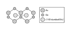
- FIG. 1 is a schematic view showing a ⁇ 110> dumbbell formed between GsAs crystal lattices.
- FIG. 2 is a schematic diagram showing that stabilizing the ⁇ 110> dumbbell suppresses clustering of interstitial As.
- FIG. 3 is a graph showing the formation energy in the neutral state of the ⁇ 110> dumbbell in GaAs and AlAs.
- FIG. 4 is a graph showing the binding energy in the neutral state of the ⁇ 110> dumbbell in GaAs and AlAs.
- FIG. 5 is a diagram illustrating a group III site, a group V site, a closest position of a dumbbell, and a second adjacent position of the dumbbell.
- FIG. 1 is a schematic view showing a ⁇ 110> dumbbell formed between GsAs crystal lattices.
- FIG. 2 is a schematic diagram showing that stabilizing the ⁇ 110> dumbbell suppresses clustering of interstitial As.
- FIG. 3 is a graph showing the formation energy in the neutral
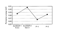
- FIG. 6 is a graph showing the formation energy of ⁇ 110> dumbbells in an In 0.6 Ga 0.4 As mixed crystal in a neutral state.
- FIG. 7 is a graph showing the formation energy of ⁇ 110> dumbbells in GaAs.
- FIG. 8 is a graph showing the size of the diffusion barrier between the lattices As.
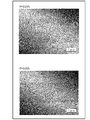
- FIG. 9 is a diagram showing an observation image by TEM.
- FIG. 10 is a schematic diagram illustrating the semiconductor device according to the first embodiment.
- FIG. 11 is a graph showing the slope efficiency of the semiconductor laser device when the concentration of P in the active layer is changed.
- FIG. 12 is a schematic view showing a semiconductor device according to the second embodiment.
- FIG. 13 is a schematic view showing a semiconductor device according to the third embodiment.
- FIG. 14 is a schematic view showing a semiconductor device according to the fourth embodiment.
- FIG. 15 is a schematic view showing a semiconductor device according to the fifth embodiment.
- FIG. 16 is a schematic view showing a semiconductor device according to the sixth embodiment.
- FIG. 17 is a schematic view showing a semiconductor device according to the seventh embodiment.
- FIG. 18 is a schematic view showing a semiconductor device according to the eighth embodiment.
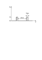
- FIG. 19 is a diagram showing an example in which P atoms are introduced digitally.
- gallium arsenide (GaAs) or aluminum arsenide (AlAs) is used as an example of a semiconductor crystal, but the implementation of the present invention is not limited to these examples, and III containing arsenic (As) as a main component.
- the present invention can be appropriately implemented in a semiconductor device using a ⁇ V group semiconductor crystal.
- the group III-V semiconductor crystal containing As as a main component includes AlGaAs, InGaAs, AlGaInAs, GaInNAs, AlGaInNAs, and the like.
- As being a V group main component means that the ratio of As to all V group elements in the composition elements of the III-V group semiconductor crystal is 95% or more.
- Al or Ga is a group III main component means that the ratio of Al or Ga to all group III elements in the composition elements of the group III-V semiconductor crystal is 95% or more.
- dislocation loop growth suppression mechanism First, let us consider the mechanism of dislocation loop formation. At that time, assuming uniform nucleation, the energy for forming dislocation loops in GaAs is the self energy of dislocations (sum of linear tension, dislocation core, and entropy term), stacking fault energy, and point defects. It depends on the balance between the degree of supersaturation and the chemical potential determined by the temperature of the system. However, when the formation energy was calculated using known physical quantities, it became clear that homogeneous nucleation was not a dislocation loop formation mechanism.
- Non-Patent Document 1 describes the relationship between the strain amount of a system and the structure of a point defect complex by performing heat treatment after growth on GaAs grown by a low temperature molecular beam epitaxy method. That is, the As interstitial atoms introduced during crystal growth progress to an assembly of As interstitial atom pairs, four interstitial As, and eight interstitial As with increasing heating temperature. . The strain of the system decreases as the aggregate of As interstitial atoms increases. This result means that the distortion of the entire system is alleviated by the formation of interstitial As clusters.
- the relaxation of strain originates from the presence of minute dislocation loops on the nanometer scale around the clusters present in the matrix. Such a small dislocation loop cannot be observed using a transmission electron microscope (TEM) or the like. However, when this dislocation loop grows by absorbing supersaturated point defects existing around it, its existence becomes obvious. When the growth of the dislocation loop further proceeds, the semiconductor device may eventually deteriorate and be destroyed. In particular, when a high load is applied to a semiconductor device, such as a high-power laser drive or a high electric field application, interstitial atoms are easily generated in the semiconductor crystal, and the interstitial atoms are easy to move. Growth is promoted. Such a dislocation loop grows in the bulk and causes deterioration of the characteristics of the semiconductor device.
- TEM transmission electron microscope
- FIG. 1 is a schematic view showing a ⁇ 110> dumbbell formed between GsAs crystal lattices.
- GaAs has a zinc blende type crystal structure composed of gallium atoms (Ga) and arsenic atoms (As).
- Ga gallium atoms
- As arsenic atoms
- the ⁇ 110> dumbbell is stable with As interstitial atoms paired in the ⁇ 110> direction.
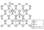
- FIG. 2 is a schematic diagram showing that stabilizing the ⁇ 110> dumbbells suppresses the clustering of interstitial As in the (1-10) plane.
- FIG. 2 corresponds to an example in which phosphorus (P) is introduced into a group V site of a GaAs crystal lattice to be verified later, but ⁇ 110> dumbbell stabilization and interstitial As clustering suppression. The relationship is not limited to the case where P is introduced into the group V site.
- dumbbell stabilization contributes to the suppression of the generation of dislocation loops.
- the introduced impurity is a group III element or a group V element from the viewpoint of not adversely affecting electrical characteristics.
- the degree to which the ⁇ 110> dumbbell is stabilized depending on the type and position of atoms introduced, including not only P but also atoms such as nitrogen (N), indium (In), antimony (Sb), etc. will be verified. .
- E form per unit cell of the ⁇ 110> dumbbell depends on the charge state q and Fermi energy E f of the system, and is expressed by the following equation (2).
- E form (q, E f ) E tot [dumbbell] (q) ⁇ E tot [bulk] ⁇ n + qE f (2)
- ⁇ n is the chemical potential of the element n.
- ⁇ n has a different value depending on whether the growth condition is a group III (Ga / Al) rich condition or a group V (As) rich condition.
- E tot becomes the total energy E tot [dumbbell + impurity] (q) of the system including the impurity, and the addition of impurity atoms and the removal of Ga (Al) or As atoms are considered in terms of chemical potential.
- the impurity means an element such as P, N, Sb, or In introduced into the GaAs crystal or the AlAs crystal in order to suppress the formation of clusters of As interstitial atoms.
- the binding energy of the ⁇ 110> dumbbell was defined as the total energy of the system when the ⁇ 110> dumbbell was formed and the difference between the total energy of the system when two As interstitial atoms separated from each other existed.
- the main calculation conditions are as follows.
- ⁇ Atom model 64 atoms (Ga or Al: 32, As: 32) constituting the matrix, As atoms constituting dumbbells: 2, Impurity atoms introduced: 1 to 3 Cut-off energy: Wave function And charge density distribution, 30 Ry and 250 Ry, respectively
- K point sample 3 ⁇ 3 ⁇ 2 -Calculated number of bands: 200
- JAMSEC Japan Agency for Marine-Earth Science and Technology
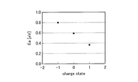
- FIG. 3 is a graph showing the formation energy in a neutral state of ⁇ 110> dumbbells in GaAs and AlAs (Group III rich condition). Similar results can be obtained even under the V group rich condition.
- the vertical axis represents ⁇ 110> dumbbell formation energy (eV)
- the horizontal axis represents the type of element to be introduced.
- the results in GaAs are indicated by black circles, and the results in AlAs are indicated by hollow squares.
- FIG. 4 is a graph showing the binding energy in the neutral state of the ⁇ 110> dumbbell in GaAs and AlAs.
- the vertical axis represents the ⁇ 110> dumbbell binding energy (eV)
- the horizontal axis represents the type of element to be introduced.
- the results in GaAs are indicated by black circles, and the results in AlAs are indicated by hollow squares.
- the meanings of the ellipsis shown on the horizontal axis in the graphs of FIGS. 3 and 4 are as follows.
- the group III site, the group V site, the closest position of the dumbbell, and the second adjacent position of the dumbbell are as shown in FIG. Note that due to the three-dimensionality of the crystal structure, the closest position and the second proximity position are present on the front side and the back side of the paper, respectively.
- the formation energy of the ⁇ 110> dumbbell is lower than when not introduced.
- the effect when P is introduced is remarkable, and the formation energy is reduced by about 0.2 eV.
- the formation energy of ⁇ 110> dumbbells hardly changes or increases when Al or Ga is introduced.
- the introduction of In is less effective than P, but the formation energy decreases.
- the effect of reducing the formation energy becomes remarkable and a synergistic effect is obtained.
- the effect of reducing the formation energy is greater than the introduction of either N or P, and a synergistic effect is obtained.
- the effect of reducing dumbbell formation energy becomes remarkable when a plurality of P is introduced.
- the formation energy is reduced by about 0.3 eV.
- the effect is large in the model 3P (introduction of two P at the closest position of the dumbbell and one P at the second adjacent position).
- FIG. 6 is a graph showing the formation energy of ⁇ 110> dumbbells in an In 0.6 Ga 0.4 As mixed crystal in a neutral state. Calculations are performed under Group III rich conditions. In addition, in the group III site in the lattice, the In atom and the Ga atom are assumed to be randomly arranged.
- the vertical axis indicates the formation energy (eV) of ⁇ 110> dumbbells
- the horizontal axis indicates the type of element to be introduced.
- Model dumbbell-1 and model dumbbell-2 shown on the horizontal axis represent cases where In atoms and Ga atoms are arranged at the closest positions of the ⁇ 110> dumbbell, respectively.
- Model P-1 and model P-2 are obtained by introducing P into model dumbbell-1 and model dumbbell-2, respectively.
- the formation energy of the ⁇ 110> dumbbell decreases by about 20-30 meV.
- a model dumbbell-1 and a model P-1 having lower formation energy are formed in the vicinity of In atoms. This is because the effective shell charge of In atoms is high.
- InGaAs mixed crystals reflect the contribution of the effective shell charge of the In atoms constituting the matrix more greatly than GaAs and AlAs, as described above, so that the energy of ⁇ 110> dumbbell formation is 0 compared to GaAs and AlAs. It has decreased by about 1 to 0.25 eV. This means that in an AlGaAs mixed crystal, the concentration of As interstitial atoms alone is likely to be higher than in an InGaAs mixed crystal, and As clusters are likely to be formed, and the effect of introducing the impurities is higher. .
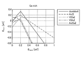
- FIG. 7 is a graph showing the formation energy of ⁇ 110> dumbbells in GaAs (Ga-rich condition).
- the slope is a charged state, which is a donor when positive and an acceptor when negative.
- FIG. 7 shows other interstitial defects such as As interstitial atoms (As ⁇ I ⁇ ), Ga vacancies (V ⁇ Ga ⁇ ), As vacancies (V ⁇ As ⁇ ), As antisites.
- a graph of defects (As ⁇ Ga ⁇ ) is also shown.
- the graph of ⁇ 110> dumbbell formation energy and the graph of formation energy of As interstitial atoms intersect at a position where the Fermi energy is approximately 0.35 eV. Therefore, when the Fermi energy is higher than 0.35 eV, the formation energy of the ⁇ 110> dumbbell is lower than the formation energy of As interstitial atoms.
- the band gap of GaAs obtained by simulation is about 1 eV, and the Fermi energy in the intrinsic semiconductor is about 0.5 eV.
- the crossing of the formation energy of As interstitial atoms and the formation energy of ⁇ 110> dumbbell at 0.35 eV indicates that the ⁇ 110> dumbbell is stable unless a p-type impurity is intentionally added.
- the Fermi energy is about 0.5 eV, the formation energy of Ga vacancies and As vacancies that are acceptors is low, and if there are residual impurities such as carbon, the Fermi energy decreases.
- the n-type dopant concentration may be an amount that can cancel the compensation effect due to vacancies and residual impurities. For example, it is desirably 1 ⁇ 10 15 cm ⁇ 3 or more. Even if such a mixed crystal having n-type conductivity is formed as an n-type conductive region inside a region to function as a p-type semiconductor in a semiconductor device, for example, the n-type conductive region Among them, the effect that As interstitial atoms form ⁇ 110> dumbbells is more stable.
- Examples of n-type dopants include silicon (Si) and selenium (Se).
- FIG. 8 is a graph showing the size of the diffusion barrier of the interstitial As.
- the barrier Ea for the diffusion of a single As interstitial atom depends on the charged state, and is about 0.8 eV when the charged state is ⁇ 1 (in GaAs having n-type conductivity).
- the charge state is +1 (in GaAs having p-type conductivity)
- it is about 0.4 eV. That is, the barrier against diffusion of a single As interstitial atom is twice or more larger in GaAs having n-type conductivity than in GaAs having p-type conductivity.
- the example of GaAs in which no impurity is introduced has been described, but the same effect is obtained even when an impurity is introduced.
- the As interstitial diffusion barrier increases by about 10% (in the neutral state, increases by 50 meV). That is, the effect of suppressing the diffusion of As interstitial atoms becomes more remarkable by introducing P into GaAs and making the base conductivity n-type.
- Table 1 shown below is a table summarizing experimental results verifying the relationship between the concentration of P substituted at the group V element site, the formation of dumbbells, and the detection of As precipitates.
- the verification experiment shown in Table 1 is performed as follows.
- SIMS Secondary ion mass spectrometry
- primary ions beam-like ions
- secondary ions ions generated by collisions between the ions and the solid surface at the molecular / atomic level. It is a surface measurement method to detect with.
- SIMS has a spatial resolution of about 10 ⁇ m, but can quantitate P with a concentration of about 0.01%.
- SIMS is preferably used for, for example, a GaAs long cavity laser element.
- An example of a measuring apparatus that employs SIMS is Cameca's sector SIMS (IMS series).
- the atom probe method is used to measure the concentration of P.
- a region including a measurement target is processed into a needle shape (probe shape) using a focused ion beam (FIB) processing apparatus.
- FIB focused ion beam
- the constituent atoms are field evaporated from the tip of the sample processed into a probe shape, and the atomic mass is analyzed by measuring the time of flight of the field evaporated atoms.
- the atom probe method is used for a semiconductor, it is preferable to assist evaporation of atoms with a laser beam in order to prevent charge-up.
- This measuring method is suitable, for example, for measuring the P concentration in the active layer in an InP-based BH laser element. This is because the analysis range can be narrowed (for example, 1 ⁇ m or less) as compared with normal SIMS.
- An example of a measuring apparatus that employs this atom probe method is Cameca's LEAP series.
- the concentration of P is measured using a scanning tunneling microscope (STM).
- STM scanning tunneling microscope
- the measurement method using STM is suitable for both InP-based BH laser elements and GaAs-based ridge laser elements.
- a sample is cleaved in an ultrahigh vacuum to expose a cross section of the active layer, and an atomic image is observed by STM.
- STM applies a bias voltage of several volts between a probe whose tip curvature is on the order of nanometers and the sample surface, and feeds back a small tunnel current (about 1 nA or less), thereby obtaining an uneven image of atoms. It is a microscope. At this time, since the electronic state is different between the base Ga, As, etc. and P, there is a difference in the contrast of the image obtained by STM. Therefore, the concentration can be evaluated by counting the number of P atoms from the image obtained by STM. Examples of STMs that can be used in this measurement method include STM-1 and LT-STM manufactured by Omicron.
- the concentration of P can be determined from the measurement of the optical band gap by photoluminescence measurement or the measurement of the lattice constant by X-ray diffraction.
- ⁇ 110> dumbbells can be confirmed by, for example, Raman spectroscopic measurement. This is because a crystal in which ⁇ 110> dumbbells are formed has a Raman-active vibration mode caused by ⁇ 110> dumbbells. For example, using a third harmonic of an Ar ion laser with a wavelength of 488 nm or a YAG laser with a wavelength of 355 nm, the local vibration mode is measured at a position of 50 to 150 cm ⁇ 1 with respect to the LO mode of the mixed crystal constituting the active layer. By doing so, formation of ⁇ 110> dumbbells can be confirmed.
- dumbbells As a method for directly observing the formation of ⁇ 110> dumbbells, there is anisotropy measurement of strain by X-ray diffraction. This method enables high-precision measurement by using wavelength-variable radiation. After the waveguide structure on the active layer is removed by etching, the dependency of the lattice constant on the depth direction is measured by measuring a plurality of diffraction surfaces.
- the precipitate of As As for the precipitate of As, observation with a transmission electron microscope (TEM) is performed. Quantification of As precipitates is based on the number of observations based on a resonator length of 100 ⁇ m in a resonator having a width of 25 ⁇ m. For example, as shown in FIG. 9, when TEM observation is performed, the presence of As precipitates is recognized as in the broken-line circle. By quantifying the As precipitates detected in this way around a resonator length of 100 ⁇ m, the As precipitate is quantified. In addition, in the observation image by TEM shown in FIG. 9, the concentration of P is 0.01% or less (meaning that P is not substantially added, the same applies hereinafter) and the concentration of P is 0.02%. In this case, a part of the measurement range is cut out.
- TEM transmission electron microscope
- the local vibration mode due to the ⁇ 110> dumbbell is observed when the concentration of P in the crystal is 0.01% and 0.02%.
- the concentration of P in the crystal is 0.1% or more, it is considered that the stabilization of interstitial As by the ⁇ 110> dumbbells functions sufficiently.
- the concentration of P, N, or Sb substituted at the group V element site is preferably in the range of 0.02% or more with respect to the total amount of the group V element at the group V element site, 0.1% It is more preferable to be in the above range.
- the concentration of In substituted for the Group III element site is the entire Group III element at the Group III element site.
- a range of 0.1% or more with respect to the amount is preferable. In this range, the probability that the introduced impurity atoms are close to other P impurity atoms increases, and the model 2P-1 ( ⁇ 110> dumbbell closest position and the second position indicated on the horizontal axis in FIGS. This is because it is easy to realize a state in which P is arranged at a close position.
- the concentration of impurity atoms in the group V element is in the range of 0.1 to 5%, the formation energy of ⁇ 110> dumbbells is low and the binding energy is high.
- the concentration of impurity atoms added to the III-V group semiconductor crystal containing As as a main component is preferably 5% or less. This is because the initial characteristics are excellent when the impurity atom concentration is 5% or less.
- the initial characteristic is evaluated by the maximum value of the slope efficiency when the temperature is changed.
- the slope efficiency is defined by the slope of the current-light output characteristic, and its unit is [mW / mA].
- Table 2 summarizes the verification results of the initial characteristics. As shown in Table 2, it can be seen that the initial characteristics are excellent when the concentration of impurity atoms is 5% or less. In particular, if the concentration of impurity atoms is 3% or less, no deterioration in the initial characteristics is measured.
- the energization and the current-light output characteristic measurement are repeated, and the increase rate of the threshold is measured.
- the increase rate of the threshold was measured under the acceleration condition of 120 ° C./150 mA
- the gradual deterioration was suppressed in the cases where the P concentration was 0.02%, 3%, and 5%.
- the increase rate of the threshold was measured under the acceleration condition of 155 ° C./125 mA
- the gradual deterioration was suppressed when the P concentration was 0.02% and 3%. Therefore, if the concentration of impurity atoms is 5% or less, the gradual deterioration is suppressed, and it is more preferable if the concentration of impurity atoms is 3% or less.
- the impurity atom concentration is 5% or less, the lattice constant difference and the band gap difference with the mixed crystal substrate are not large, so that the mobility is reduced due to misfit dislocation formation or alloy scattering, or two-dimensional electrons.
- the concentration is desirably 1% or less. This is because, when the concentration is higher than 1%, In is clustered and formation of ⁇ 110> dumbbells is prevented.
- the concentration of P, N, or Sb substituted at the group V element site is in the range of 0.02% to 5% with respect to the total amount of the group V element at the group V element site. It is preferable that it is 0.1% or more and 3% or less.
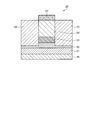
- FIG. 10 is a schematic diagram illustrating the semiconductor device according to the first embodiment.
- the semiconductor device shown in FIG. 10 is a semiconductor laser element using a buried heterostructure (BH) structure as a current confinement structure.
- FIG. 10 is a cross-sectional view parallel to the emission surface of this semiconductor laser element.
- BH buried heterostructure
- an n-type semiconductor layer 12 and an active layer 13 are sequentially stacked on a substrate 11.
- the upper part of the n-type semiconductor layer 12 and the active layer 13 have a mesa structure having a longitudinal direction in the emission direction.
- the active layer 13 has a multiple quantum well (MQW) structure including a well layer and a barrier layer.
- MQW multiple quantum well
- a p-type semiconductor layer 14 is laminated on the top of the n-type semiconductor layer 12 and the mesa structure formed of the active layer 13.
- An n-type semiconductor layer 15 as a current confinement structure is formed inside the p-type semiconductor layer 14 adjacent to both sides in the width direction of the mesa structure.
- an n-side electrode 16 is formed on the back surface of the substrate 11, and a p-side electrode 17 is formed on the surface of the p-type semiconductor layer 14.
- the n-type semiconductor layer 15 as a current confinement structure confines the current injected from the p-side electrode 17 inside, and confines the light generated from the active layer 13 in the lateral (width) direction, so that a high-order horizontal transverse mode is obtained. Responsible for the function to realize single transverse mode operation with suppressed.
- the well layer of the active layer 13 is a layer made of InGaAsP in which P is introduced into InGaAs.
- the barrier layer of the active layer 13 is made of AlGaAs and serves as a barrier function for confining carriers in the well layer.
- the active layer 13 is not limited to the above example, and may be formed of a III-V group semiconductor mainly composed of As such as GaAs, AlAs, AlGaAs, InGaAs, AlGaInAs, and GaInNAs.
- P is introduced only into the well layer of the active layer 13.
- P may be introduced into AlGaAs as the barrier layer, and P may be introduced into the entire active layer 13.
- the configuration of the active layer 13 is not limited to the multi-well structure, and any structure of the active layer 13 can suppress the occurrence of dislocation loops by introducing P.
- the impurity to be introduced is not limited to P, but may be N, Sb, or In.
- the active layer 13 Since the active layer 13 is in an active state when the semiconductor laser device 10 is driven, As interstitial atoms are easily formed and the As interstitial atoms are easily moved. Therefore, P, N, Introducing Sb or In is highly effective. In particular, when the active layer 13 has a multiple quantum well structure, it is the well layer that is activated when the semiconductor laser device 10 is driven. Therefore, P, N, Sb, or In is selectively applied only to the well layer. The effect is also great by introducing.
- the active layer 13 preferably has n-type conductivity. Therefore, it is preferable to add an n-type dopant to the active layer 13.
- the n-type dopant includes selenium (Se), sulfur (S), or silicon (Si).
- concentration of the n-type dopant of the active layer 13 is lower than the density
- the concentration of the n-type dopant in the active layer 13 is preferably 1 ⁇ 10 18 cm ⁇ 3 or less.
- the concentration is higher than 1 ⁇ 10 18 cm ⁇ 3
- the concentration of Ga vacancies and As vacancies in the semiconductor increases, so the binding energy of adjacent ⁇ 110> dumbbells decreases, and the effect of suppressing the diffusion of As interstitial atoms is reduced. It is because it falls. Further, it is desirable that the amount is sufficient to cancel the compensation effect of vacancies and residual impurities, for example, 1 ⁇ 10 15 cm ⁇ 3 or more.
- the other semiconductor layer is formed of a semiconductor having a higher band gap energy and a lower refractive index than the well layer of the active layer 13.
- the other semiconductor layer is preferably formed of a group III-V semiconductor containing As as a main component, but may be formed of, for example, InP.
- P, N, Sb, or In is selectively introduced into the p-type semiconductor layer 14 under the p-side electrode 17 or the n-type semiconductor layer 12 near the interface with the epitaxial substrate. This is also effective in suppressing the occurrence of dislocation loops. Further, selectively making the location where the dislocation loop is likely to occur n-type conductivity is also effective in suppressing the occurrence of the dislocation loop. As described above, the effect of suppressing the occurrence of dislocation loops can be obtained even if the semiconductor layer 10 has n-type conductivity as much as the intrinsic semiconductor.
- the semiconductor laser element 10 By creating a weak n-type conductive region that does not affect the function of the dislocation loop, the effect of suppressing the occurrence of dislocation loops can be obtained.
- Example 1 is a configuration embodying the first embodiment. Therefore, in the description of the first embodiment, the same FIG. 10 as that of the first embodiment is referred to. Moreover, the description which overlaps with description of 1st Embodiment is abbreviate
- the semiconductor laser device 10 according to Example 1 is a so-called AlInGaAsP-BH laser device on an InP substrate. Therefore, an n-type semiconductor layer 12 made of, for example, n-type InP and an active layer 13, for example, a p-type semiconductor layer 14 made of, for example, p-type InP are stacked on a substrate 11 made of InP.
- the active layer 13 has a mesa structure.
- the active layer 13 has an MQW structure in which a pair of a well layer and a barrier layer is laminated six times.
- a resonator width stripe width of the active layer 13
- a resonator length stripe length of the active layer 13
- the thicknesses of the well layer and the barrier layer are 6 nm and 10 nm, respectively, and the strain of the well layer and the barrier layer with respect to the InP substrate is 1% and ⁇ 0.3%, respectively.
- substrate is set as a positive distortion
- the case where it is small is set as a negative distortion.
- the composition of the active layer and the barrier layer of the active layer 13 is adjusted so that the oscillation wavelength is 1.55 ⁇ m.
- the composition of the active layer 13 in the case of different P concentrations is illustrated.
- the well layer is Al 0.058 In 0.676 Ga 0.267 As and the barrier layer is Al 0.206 In 0.488 Ga 0.306 As.
- the well layer is Al 0.054 In 0.68 Ga 0.265 As 0.99 P 0.01
- the barrier layer is Al 0.203. In 0.49 Ga 0.307 As 0.99 P 0.01 .
- the structure of the active layer 13 is such that the well layer is Al 0.048 In 0.69 Ga 0.262 As 0.97 P 0.03 , and the barrier layer Is Al 0.2 In 0.6 Ga 0.2 As 0.97 P 0.03 .
- the composition of group III Al, Ga, and In
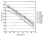
- FIG. 11 is a graph showing the slope efficiency of the semiconductor laser device when the concentration of P in the active layer is changed.
- data of two semiconductor laser elements having the same structure and composition are shown by a solid line and a broken line.
- the maximum value of the slope efficiency does not change until the concentration of P in the active layer is 3%.
- the maximum value of the slope efficiency at 25 ° C. is 0.28 to 0.29 mW / mA.
- the concentration of P in the active layer exceeds 5%, the slope efficiency decreases.
- the concentration of P in the active layer is 6.6%
- the maximum value of the slope efficiency at 25 ° C. is 0.22. It is ⁇ 0.23 mW / mA.
- the concentration of P in the active layer exceeds 10%, the slope efficiency at 25 ° C. is significantly lowered and becomes 0.2 mW / mA. Therefore, the semiconductor laser device 10 according to Example 1 has excellent initial characteristics.
- the threshold value of the active layer semiconductor laser element not added with P increases gradually after 1000 hours and increases by 10% or more after 2000 hours.
- the concentration of P in the active layer is 0.02%, 2.9%, and 6.6%, the gradual deterioration of the semiconductor laser element is suppressed.
- the increase rate of the threshold at 2000 hours is also 8% or less.
- the tendency of the threshold increase does not change, and the increase of the threshold is suppressed when the concentration is 0.02% and 2.9%, but in the example where P is not added.
- a 10% to 20% increase in threshold is measured.
- FIG. 12 is a schematic view showing a semiconductor device according to the second embodiment.
- the semiconductor device shown in FIG. 12 is a semiconductor laser element using an SI-BH (Semi-Insulating Buried Heterostructure) structure.
- FIG. 12 is a cross-sectional view parallel to the emission surface of this semiconductor laser element.
- SI-BH Semi-Insulating Buried Heterostructure
- an n-type semiconductor layer 22, an active layer 23, and a p-type semiconductor layer 24 are sequentially stacked on a substrate 21.
- the upper part of the n-type semiconductor layer 22, the active layer 23, and the p-type semiconductor layer 24 have a mesa structure having a longitudinal direction in the emission direction.
- the active layer 23 has a multiple quantum well structure including a well layer and a barrier layer.
- a buried layer 25 made of a high-resistance material such as Fe—InP is formed on the n-type semiconductor layer 22 and on both sides of the mesa structure made of the active layer 23 and the p-type semiconductor layer 24. Further, an n-side electrode 26 is formed on the back surface of the substrate 21, and a p-side electrode 27 is formed on the surface of the p-type semiconductor layer 24.
- the buried layer 25 has a function of suppressing the spread of current flowing from the p-side electrode 27 to the n-side electrode 26 and confining light generated from the active layer 23 in the lateral (width) direction.
- the buried layer 25 is made of, for example, a semi-insulating III-V semiconductor doped with iron (Fe).
- the buried layer 25 is not limited to a semi-insulating III-V semiconductor doped with iron (Fe), but may be a semi-insulating III-V semiconductor doped with ruthenium (Ru).
- the well layer of the active layer 23 is a layer made of InGaAs 0.99 P 0.01 in which P is introduced into InGaAs.
- the barrier layer of the active layer 23 is made of AlGaAs and serves as a barrier function for confining carriers in the well layer.
- the active layer 23 is not limited to the above example, and may be formed of other group III-V semiconductors mainly composed of As.
- the configuration of the active layer 23 is not limited to the multi-well structure, and P can be introduced into the entire active layer, and the impurity to be introduced is not limited to P.
- the active layer 23 preferably has n-type conductivity. Therefore, it is preferable to introduce an n-type dopant into the active layer 23.
- concentration of the n-type dopant of the active layer 23 is lower than the density
- the concentration of the n-type dopant in the active layer 23 is preferably 1 ⁇ 10 18 cm ⁇ 3 or less, and preferably 1 ⁇ 10 15 cm ⁇ 3 or more.
- the other semiconductor layer is formed of a semiconductor having a higher band gap energy and a lower refractive index than the well layer of the active layer 23.
- the other semiconductor layer is preferably formed of a group III-V semiconductor containing As as a main component, but may be formed of, for example, InP.
- P, N, Sb, or In into all the semiconductor layers of the semiconductor laser element 20
- P, N, Sb, or In is selectively applied to a portion of the p-type semiconductor layer 24 under the p-side electrode 27 or a portion of the p-type semiconductor layer 24 near the interface with the buried layer 25.
- the introduction is also effective in suppressing the occurrence of dislocation loops.
- selectively making the location where the dislocation loop is likely to occur n-type conductivity is also effective in suppressing the occurrence of the dislocation loop.
- the effect of suppressing the occurrence of dislocation loops can be obtained even if the semiconductor layer 20 has n-type conductivity as much as the intrinsic semiconductor. Therefore, even if it is a p-type semiconductor layer of the semiconductor laser element 20, the semiconductor laser element 20 By creating a weak n-type conductive region that does not affect the function of the dislocation loop, the effect of suppressing the occurrence of dislocation loops can be obtained.
- FIG. 13 is a schematic view showing a semiconductor device according to the third embodiment.
- the semiconductor device shown in FIG. 13 is a semiconductor laser element using a ridge structure.
- FIG. 13 is a cross-sectional view parallel to the emission surface of this semiconductor laser element.
- an n-type semiconductor layer 32, an active layer 33, and a p-type semiconductor layer 34 are sequentially stacked on a substrate 31.
- the upper part of the p-type semiconductor layer 34 has a ridge structure having a longitudinal direction in the emission direction.
- the active layer 33 has a multiple quantum well structure including a well layer and a barrier layer.
- an IFVD (Impurity Free Vacancy Disordering) method which is an end face protection structure described in Patent Document 1, is applied to the active layer 33.
- the ridge structure bears the function of confining light generated from the active layer 33 in the lateral (width) direction by making a difference in the thickness of the p-type semiconductor layer 34 functioning as a cladding layer.
- An n-side electrode 36 is formed on the back surface of the substrate 31, and a p-side electrode 37 is formed on the surface of the p-type semiconductor layer 34.
- the well layer of the active layer 33 is a layer made of InGaAsP in which P is introduced into InGaAs.
- the barrier layer of the active layer 33 is made of AlGaAs and serves as a barrier function for confining carriers in the well layer.
- the active layer 33 is not limited to the above example, and may be formed of other group III-V semiconductors mainly composed of As. Further, similarly to the first embodiment, in this embodiment, the configuration of the active layer 33 is not limited to the multiple well structure, and P can be introduced into the entire active layer, and the impurity to be introduced is not limited to P.
- the active layer 33 preferably has n-type conductivity. Therefore, it is preferable to introduce an n-type dopant into the active layer 33.
- concentration of the n-type dopant of the active layer 33 is lower than the density
- the concentration of the n-type dopant in the active layer 33 is preferably 1 ⁇ 10 18 cm ⁇ 3 or less, and preferably 1 ⁇ 10 15 cm ⁇ 3 or more.
- the other semiconductor layer is formed of a semiconductor having a higher band gap energy and a lower refractive index than the well layer of the active layer 33.
- the other semiconductor layer is preferably formed of a group III-V semiconductor containing As as a main component, but may be formed of, for example, InP.
- P, N, Sb, or In is introduced into all the semiconductor layers of the semiconductor laser element 30, not only the active layer 33 but also P, N, A method of introducing Sb or In is also conceivable.
- P, N, Sb, or In is selectively introduced into a portion of the p-type semiconductor layer 34 under the p-side electrode 37 or a portion of the p-type semiconductor layer 34 that becomes the rising portion of the ridge structure. This is also effective in suppressing the occurrence of dislocation loops. Further, selectively making the location where the dislocation loop is likely to occur n-type conductivity is also effective in suppressing the occurrence of the dislocation loop.
- the effect of suppressing the occurrence of dislocation loops can be obtained even if the semiconductor layer 30 has an n-type conductivity as much as the intrinsic semiconductor. Therefore, even if it is a p-type semiconductor layer of the semiconductor laser element 30, the semiconductor laser element 30 By creating a weak n-type conductive region that does not affect the function of the dislocation loop, the effect of suppressing the occurrence of dislocation loops can be obtained.
- the IFVD method when the laser output is about 1 W or less, the deterioration mode due to the end face is suppressed without adding P, N, Sb, or the like.
- the semiconductor laser device 30 in addition to the IFVD method being applied, P, N, Sb, or the like is introduced into the active layer 33 or the like, so that the CW having an optical output of several tens W or more Even under driving conditions, the occurrence of dislocation loops in the bulk as well as the end face is suppressed.
- Example 2 is a configuration embodying the third embodiment. Therefore, in description of Example 2, FIG. 13 same as 3rd Embodiment is referred. Moreover, the description which overlaps with description of 1st Embodiment is abbreviate
- the semiconductor laser device 30 according to the second embodiment is a ridge laser device on a so-called GaAs substrate. Therefore, an n-type semiconductor layer 32 made of, for example, n-type AlGaAs and an active layer 33, eg, a p-type semiconductor layer 34 made of, for example, p-type AlGaAs are stacked on a substrate 31 made of GaAs.
- the ridge structure has a longitudinal direction in the emission direction.
- the active layer 33 has an SQW (Single Quantum Well) structure in which a well layer is sandwiched between barrier layers.
- SQW Single Quantum Well
- a light output of about 12 W can be achieved with one chip when the drive (rated) current is 12 A.
- the thicknesses of the well layer and the barrier layer are 10 nm and 30 nm, respectively, and P is added to the active layer while adjusting the composition of the well layer and the barrier layer so that the oscillation wavelength is 910 nm.
- an oscillation wavelength of 910 nm can be realized by setting the well layer to In 0.075 Ga 0.925 As and the barrier layer to Al 0.32 Ga 0.68 As. Further, in the example of the active layer to which P is added at a concentration of 3%, the well layer is In 0.1 Ga 0.9 As 0.97 P 0.03 , and the barrier layer is Al 0.31 Ga 0.69 As. An oscillation wavelength of 910 nm can be realized by setting 0.97 P 0.03 . In this way, the Group III composition is adjusted, and the concentration of P added so as to make the wavelength constant is changed in the range of 0.02 to 10%.
- the initial characteristics are evaluated using a semiconductor laser device in which the concentration of P added as described above is changed in the range of 0.02 to 10%.
- the initial characteristics are evaluated by the maximum value of the slope efficiency at room temperature (25 ° C.).
- the slope efficiency is in the range of 1.01 to 1.02 W / A in any semiconductor laser element including the case where P is not added. Good initial characteristics can be obtained.
- the slope efficiency is reduced to about 1 W / A.
- the slope efficiency is reduced to 0.9 W / A or less.
- the semiconductor laser device it is desirable to configure the semiconductor laser device so that the concentration of P added to the active layer is 3% or less.
- the optical output of the semiconductor laser element was monitored while energizing a constant current of 12 A at an ambient temperature of 25 ° C.
- the optical output was exceeded after 1000 hours in the semiconductor laser element in which P was not added to the active layer. Decrease is observed.
- the semiconductor laser device in which P is added to the active layer at a concentration of 0.02% the light output is not reduced until 2000 hours.
- the semiconductor laser device in which P is added to the active layer at a concentration of 0.1% or more no decrease in light output is observed even after 2000 hours.
- Example 3 is obtained by changing the composition of the active layer in the configuration of Example 2. Therefore, only the composition of the active layer will be described here, and description of other components will be omitted.
- the active layer in Example 3 includes Al in the well layer and In in the barrier layer.
- the well layer is made of Al 0.05 In 0.15 Ga 0.8 As 0.97 P 0.03
- the barrier layer is made of Al 0.35 In 0.05.
- Ga 0.6 As 0.97 P 0.03 an oscillation wavelength of 910 nm is realized.
- the group III composition is adjusted, and the concentration of P added so as to make the wavelength constant is changed in the range of 0.02 to 10%.
- Example 3 the initial characteristics at room temperature (25 ° C.) are evaluated.
- the slope efficiency is in the range of 1.01 to 1.02 W / A in any semiconductor laser element including the case where P is not added.
- Good initial characteristics can be obtained. That is, the initial characteristic value at 25 ° C. is not significantly different between Example 2 and Example 3.
- the value of the initial characteristic at 50 ° C. is superior to that of the semiconductor laser device of Example 3 over Example 2. That is, the slope efficiency of Example 3 is improved by about 5% compared to the semiconductor laser element of Example 2. This is presumably because the band gaps of the well layer and the barrier layer were designed to be the same in Example 2 and Example 3, but the difference in group III composition between them caused a difference in electron affinity. The difference is 15 meV for the well layer and 19 meV for the barrier layer. As a result, in Example 3, it is considered that carrier leakage from the well layer at a high temperature was suppressed, and the slope efficiency was improved.
- Examples 2 and 3 an example of a semiconductor laser device having an oscillation wavelength of 910 nm is shown.
- the composition of the group III element may be changed as appropriate.
- the well layer of the active layer is made of Al 0.05 In 0.25 Ga 0.7 As 0.97 P 0.03
- the barrier layer is made of Al 0. 35 In 0.05 Ga 0.6 As 0.97 P 0.03 may be used.
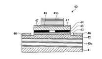
- FIG. 14 is a schematic view showing a semiconductor device according to the fourth embodiment.
- the semiconductor device shown in FIG. 14 is a vertical cavity surface emitting laser (VCSEL) type semiconductor laser element (hereinafter referred to as a surface emitting laser element).
- VCSEL vertical cavity surface emitting laser
- FIG. 14 is a cross-sectional view of the semiconductor laser element with respect to the emission direction.
- a layer 48 and an upper DBR mirror 49b are sequentially stacked.
- the upper end portion of the n-type semiconductor layer 42, the active layer 43, the current confinement layer 45, and the p-type semiconductor layer 44 are formed as mesa posts formed into a columnar shape by an etching process or the like. Yes.
- the n-side electrode 46 is disposed on the surface of the n-type semiconductor layer 42 exposed as a mesa post, and the p-side electrode 47 surrounds the phase adjustment layer 48 on the surface of the p-type semiconductor layer 44 that is the upper end of the mesa post. It is installed like a ring.
- the lower DBR mirror 49a is formed as a semiconductor multilayer mirror in which a plurality of composite semiconductor layers made of, for example, AlAs / GaAs are stacked.
- the thickness of each layer constituting this composite semiconductor layer is ⁇ / 4n ( ⁇ : oscillation wavelength, n: refractive index).
- the upper DBR mirror 49b is formed as a dielectric multilayer mirror in which a plurality of composite dielectric layers made of, for example, SiN / SiO 2 are stacked, and the thickness of each layer is ⁇ / 4n as in the lower DBR mirror 49a. It is said that.
- the current confinement layer 45 is composed of an opening and an oxidized constriction.
- the current confinement layer 45 is formed by an Al-containing layer made of, for example, AlAs, and the oxidized constriction portion is formed by oxidizing the Al-containing layer by a predetermined range from the outer peripheral portion.
- the oxidized constriction portion has an insulating property, and the current density in the active layer 43 is increased by constricting the current injected from the p-side electrode 47 and concentrating it in the opening.
- the active layer 43 has a multiple quantum well structure including a well layer and a barrier layer, and emits emitted light based on a current injected from the p-side electrode 47 and constricted by the current confinement layer 45.
- the emitted light is amplified by being resonated and amplified in a direction perpendicular to each layer including the active layer 43 between the lower DBR mirror 49a and the upper DBR mirror 49b as a resonator, and then laser is emitted from the upper surface of the upper DBR mirror 49b. Injected as light.
- the phase adjustment layer 48 provided between the p-type semiconductor layer 44 and the upper DBR mirror 49b is for adjusting the positions of antinodes and nodes of the standing wave of the laser beam formed in the resonator. is there.
- the well layer of the active layer 43 is a layer made of InGaAs 0.99 P 0.01 in which P is introduced into InGaAs.
- the barrier layer of the active layer 43 is made of AlGaAs and serves as a barrier function for confining carriers in the well layer.
- the active layer 43 is not limited to the above example, and may be formed of other group III-V semiconductors mainly composed of As. Further, similarly to the first embodiment, in this embodiment, the configuration of the active layer 43 is not limited to the multi-well structure, and P can be introduced into the entire active layer, and the impurity to be introduced is not limited to P.
- the active layer 43 preferably has n-type conductivity. Therefore, it is preferable to introduce an n-type dopant into the active layer 43.
- the n-type dopant is Se, S, or Si.
- concentration of the n-type dopant of the active layer 43 is lower than the density
- the concentration of the n-type dopant in the active layer 43 is preferably 1 ⁇ 10 18 cm ⁇ 3 or less, and when it is 1 ⁇ 10 15 cm ⁇ 3 or more, the effect of suppressing the occurrence of dislocation loops becomes significant.
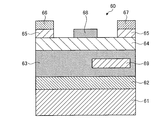
- FIG. 15 is a schematic view showing a semiconductor device according to the fifth embodiment.
- the semiconductor device shown in FIG. 15 is a heterojunction transistor (HFET).
- FIG. 15 is a cross-sectional view crossing each electrode of the heterojunction transistor.
- the heterojunction transistor 50 includes a substrate 51 made of semi-insulating GaAs and a 1 ⁇ m-thick buffer made of undoped GaAs for relaxing lattice mismatch formed on the substrate 51.
- a layer 54 and a contact layer 55 made of n + -type GaAs having a thickness of 100 nm are sequentially stacked.
- P is introduced as described above, but the same effect can be obtained by introducing Sb, N or In in addition to P. Further, In and P may be doped at the same time.
- a source electrode 56 and a drain electrode 57 are formed on the contact layer 55.
- the contact layer 55 is etched to a depth at which the surface of the electron supply layer 54 is exposed, and a gate electrode 58 is formed.
- the outline of the method for manufacturing the heterojunction transistor 50 having the above-described configuration is as follows.
- the buffer layer 52, the electron transit layer 53, the electron supply layer 54, and the contact layer 55 are sequentially epitaxially grown using the MOCVD method or the MBE method to form an epitaxial layer.
- a pattern is formed with a photoresist to protect a predetermined position, and the contact layer 55 is removed by performing wet etching on the epitaxial layer using, for example, a mixed solution of phosphoric acid, hydrogen peroxide solution, and water.
- a mixed solution of phosphoric acid, hydrogen peroxide solution, and water is exposed to form a gate electrode formation portion.
- a pattern is formed with a new photoresist, an ohmic metal made of a Ni / AuGe alloy is deposited, and lift-off is performed to form the source electrode 56 and the drain electrode 57. Further, a gate electrode 58 made of Ti / Pt / Au is formed on the surface of the electron supply layer 54 by a similar photolithography process. Thus, the heterojunction transistor 50 having the above configuration is manufactured.
- the heterojunction transistor 50 having the above configuration is excellent in long-term reliability as compared with a heterojunction transistor having a conventional structure. Specifically, the increase in on-resistance over time is suppressed, and the device life is extended. This is because P is introduced into the electron transit layer 53 in the heterojunction transistor 50. The heat generated when the heterojunction transistor 50 is energized and the concentration of the electric field between the gate and the drain at the time of interruption are likely to cause diffusion of As interstitial atoms. However, since P is introduced into the electron transit layer 53, As Diffusion of interstitial atoms is suppressed, As clusters are not formed, and as a result, generation of dislocation loops is suppressed.
- the P composition of GaAsP in the electron transit layer 53 is preferably in the range of 0.01 to 5%. Since the concentration of As interstitial atoms generated when the electric field stress applied to the device is high and characteristic variation starts to occur is about 1 ⁇ 10 19 cm ⁇ 3 , the P concentration is higher than the As interstitial atoms at this concentration. Is high (for example, 0.01% or more), the probability of ⁇ 110> dumbbell formation increases.
- FIG. 16 is a schematic view showing a semiconductor device according to the sixth embodiment.
- the semiconductor device shown in FIG. 16 is a heterojunction transistor (HFET), which is a modification of the fifth embodiment.
- FIG. 16 is a cross-sectional view crossing each electrode of the heterojunction transistor.
- this embodiment is a modification of 5th Embodiment, below, only a different point from 5th Embodiment is demonstrated.
- the heterojunction transistor 60 includes a substrate 61 made of semi-insulating GaAs and a 1 ⁇ m-thick buffer composed of undoped GaAs for relaxing lattice mismatch formed on the substrate 61.
- An electric layer composed of a layer 62, a 100 nm thick electron transit layer 63 made of undoped GaAs 0.99 P 0.01, and Al 0.3 Ga 0.7 As doped with Si, which is an n-type impurity ion.
- a supply layer 64 and a contact layer 65 made of n + -type GaAs having a thickness of 100 nm are sequentially stacked.
- a partial n-type layer 69 made of GaAs 0.99 P 0.01 having n ⁇ -type conductivity is formed in a part of the electron transit layer 63.
- the partial n-type layer 69 may be formed, for example, at a thickness of 30 nm, for example, in the intermediate portion of the electron transit layer 63 in the thickness (longitudinal) direction of the epitaxial layer. Further, in the lateral direction, it may be formed at the lower part between the gate and the drain where the electric field concentration is likely to occur and the concentration of As interstitial atoms is increased.
- the partial n-type layer 69 may be formed by selective growth or ion implantation.
- the concentration of the n-type dopant in the partial n-type layer 69 is preferably lower than the concentration of the n-type dopant in the other n-type semiconductor layers.
- the concentration of the n-type dopant in the partial n-type layer 69 is preferably 1 ⁇ 10 18 cm ⁇ 3 or less, and the effect is remarkable when it is 1 ⁇ 10 15 cm ⁇ 3 or more.
- the concentration is higher than 1 ⁇ 10 18 cm ⁇ 3
- the concentration of Ga vacancies and As vacancies in the semiconductor increases, so the binding energy of adjacent ⁇ 110> dumbbells decreases, and the effect of suppressing the diffusion of As interstitial atoms is reduced. It is because it falls. Further, this is because 1 ⁇ 10 15 cm ⁇ 3 or more is a sufficient amount to cancel the compensation effect of vacancies and residual impurities.
- the heterojunction transistor 60 in which the partial n-type layer 69 is provided at the position as described above has a high diffusion barrier of As interstitial atoms in the vicinity of the position where As interstitial atoms are generated, and thus suppresses fluctuations in characteristics due to diffusion. can do.
- FIG. 17 is a schematic view showing a semiconductor device according to the seventh embodiment.
- the semiconductor device shown in FIG. 17 is a radiation detection PIN diode.
- FIG. 17 is a cross-sectional view crossing each electrode of the PIN diode.
- the PIN diode 70 includes a substrate 71, a buffer layer 72 formed on the substrate 71, an i-type (Intrinsic) layer 73 formed on the buffer layer 72, and an i-type layer 73.
- the substrate 71 is made of semi-insulating GaAs.
- the buffer layer 72 is made of undoped GaAs having a thickness of 1 ⁇ m, and is a layer for relaxing lattice mismatch.
- the i-type layer 73 is an i-type semiconductor layer made of GaAs 0.99 P 0.01 having a thickness of 1 ⁇ m in which P is introduced into GaAs.
- the p-type layer 74 and the n-type layer 75 are p-type and n-type semiconductor layers formed by, for example, ion implantation, selective growth, or thermal diffusion with respect to GaAs.
- the anode electrode 76 can be Ti / Pt / Au, and the cathode electrode 77 can be Ni / Au.
- the interval between the anode electrode and the cathode electrode is, for example, 10 ⁇ m.
- the PIN diode 70 when a reverse voltage is applied to the anode electrode 76 and the cathode electrode 77, a depletion layer expands in the i-type layer 73. When radiation enters the depletion layer, electron-hole pairs are formed along the path of the radiation. If the PIN diode 70 is used, radiation can be detected by detecting the pulse current generated at this time.
- the detection sensitivity of radiation is proportional to the fifth power of the atomic number and the density
- forming a PIN diode with GaAs realizes a sensitivity of 100 times or more than that of a Si PIN diode, and the sensitivity is comparable to that of a Ge detector.
- the band gap of GaAs is larger than that of Si, it is advantageous for a Ge detector that operates stably at room temperature and must use liquid nitrogen.
- the mobility of GaAs at room temperature is about 8000 cm 2 / Vs, and a response speed five times that of Si can be expected.
- the conductivity is not affected because P is a group V element.
- the i-type layer 73 of this embodiment is not intentionally added with a p-type dopant. Therefore, the i-type layer 73 corresponds to a region where the Fermi energy in FIG. 7 is about 0.5 eV, and a state of forming a ⁇ 110> dumbbell is realized rather than an As interstitial atom being present alone.
- the concentration of the P element in the group V element in the i-type layer 73 is preferably 0.1 to 5%. If it is 0.1% or more, the effect of forming the ⁇ 110> dumbbell is high.
- FIG. 18 is a schematic view showing a semiconductor device according to the eighth embodiment.
- the semiconductor device shown in FIG. 18 is a vertical PIN diode for radiation detection.
- FIG. 18 is a cross-sectional view crossing each electrode of the vertical PIN diode.
- the vertical PIN diode 80 includes a substrate 81, a buffer layer 82 formed on the substrate 81, an i-type layer 83 formed on the buffer layer 82, and an i-type layer 83.
- the substrate 81 is made of GaAs having n-type conductivity.
- the buffer layer 82 is made of GaAs having a thickness of 1 ⁇ m having n-type conductivity, and is a layer for relaxing lattice mismatch.
- the i-type layer 83 is an i-type semiconductor layer made of GaAs 0.99 P 0.005 having a thickness of 100 ⁇ m in which P is introduced into GaAs.
- the p-GaAs layer 84 is formed in the i-GaAsP layer 83.
- An anode electrode 85 is formed on the p-GaAs layer 84, and a cathode electrode 86 is formed on the back surface of the substrate 81.
- the p-type layer 84 is a p-type semiconductor layer formed by, for example, ion implantation, selective growth, or thermal diffusion with respect to GaAs.
- the anode electrode 85 can be Ti / Pt / Au and the cathode electrode 86 can be Ni / Au.
- FIG. 19 shows the growth direction (thickness direction) of the i-type layer and the P concentration at that position. A portion where the P concentration is 0% corresponds to GaAs.
- an undoped layer is formed by alternately repeating a GaAsP layer and a GaAs layer having a composition of 0.05 at a thickness of 10 nm and 90 nm, respectively.
- a GaAsP layer By digitally forming a GaAsP layer, it is possible to form a region having a high P concentration locally. In the region where the P concentration is high, the ⁇ 110> dumbbell is formed at a position where a plurality of P atoms are present, and the formation energy decreases and the binding energy increases. For this reason, the effect of suppressing the diffusion of As interstitial atoms is enhanced. In addition, when a GaAsP layer is formed digitally, it is possible to suppress misfit dislocations and occurrence of cracks rather than stacking a uniform concentration GaAsP layer, and the crystal quality of the epitaxial film is improved.
- the vertical PIN diode 80 of this embodiment can increase the thickness of the depletion layer 10 times compared to the PIN diode 70 of the seventh embodiment, so that the sensitivity of radiation can be increased about 10 times. Further, since the cathode electrode 86 is on the back surface of the substrate 81, the element area can be reduced, and there is an advantage that integration of a two-dimensional detector or the like is facilitated. At the same time, in the vertical PIN diode 80 of the present embodiment, since P is introduced into the i-type layer, ⁇ 110> dumbbells are easily formed, and the diffusion of As interstitial atoms is suppressed. For this reason, the vertical PIN diode 80 of the present embodiment is superior in long-term reliability than the conventional PIN diode.
- the semiconductor device according to the present invention is useful as a semiconductor device with little variation in characteristics.
Landscapes
- Physics & Mathematics (AREA)
- Condensed Matter Physics & Semiconductors (AREA)
- General Physics & Mathematics (AREA)
- Electromagnetism (AREA)
- Optics & Photonics (AREA)
- Geometry (AREA)
- Semiconductor Lasers (AREA)
- Chemical & Material Sciences (AREA)
- Crystallography & Structural Chemistry (AREA)
- Light Receiving Elements (AREA)
- Junction Field-Effect Transistors (AREA)
Abstract
L'invention concerne un dispositif à semi-conducteur qui est pourvu d'une couche semi-conductrice comprenant un semi-conducteur cristallin de groupe III-V dont le composant principal est As, et un élément de groupe V autre que As étant introduit avec une concentration de 0,02 à 5 % au niveau du site du groupe V du semi-conducteur cristallin de groupe III-V dans la couche semi-conductrice. De préférence, l'élément de groupe V autre que As est N, P ou Sb, ou une combinaison de ceux-ci. Ainsi, l'invention concerne un dispositif à semi-conducteur qui empêche que des défauts ne se produisent dans le semi-conducteur cristallin non épitaxié et qui présente moins de variation des caractéristiques.
Priority Applications (2)
| Application Number | Priority Date | Filing Date | Title |
|---|---|---|---|
| JP2016507776A JPWO2015137373A1 (ja) | 2014-03-11 | 2015-03-11 | 半導体装置 |
| US15/235,756 US9960572B2 (en) | 2014-03-11 | 2016-08-12 | Semiconductor device |
Applications Claiming Priority (2)
| Application Number | Priority Date | Filing Date | Title |
|---|---|---|---|
| JP2014-047339 | 2014-03-11 | ||
| JP2014047339 | 2014-03-11 |
Related Child Applications (1)
| Application Number | Title | Priority Date | Filing Date |
|---|---|---|---|
| US15/235,756 Continuation US9960572B2 (en) | 2014-03-11 | 2016-08-12 | Semiconductor device |
Publications (1)
| Publication Number | Publication Date |
|---|---|
| WO2015137373A1 true WO2015137373A1 (fr) | 2015-09-17 |
Family
ID=54071816
Family Applications (2)
| Application Number | Title | Priority Date | Filing Date |
|---|---|---|---|
| PCT/JP2015/057093 Ceased WO2015137373A1 (fr) | 2014-03-11 | 2015-03-11 | Dispositif à semi-conducteur |
| PCT/JP2015/057094 Ceased WO2015137374A1 (fr) | 2014-03-11 | 2015-03-11 | Élément laser à semi-conducteurs |
Family Applications After (1)
| Application Number | Title | Priority Date | Filing Date |
|---|---|---|---|
| PCT/JP2015/057094 Ceased WO2015137374A1 (fr) | 2014-03-11 | 2015-03-11 | Élément laser à semi-conducteurs |
Country Status (5)
| Country | Link |
|---|---|
| US (2) | US9960572B2 (fr) |
| EP (1) | EP3118950B1 (fr) |
| JP (2) | JPWO2015137373A1 (fr) |
| CN (1) | CN106030939B (fr) |
| WO (2) | WO2015137373A1 (fr) |
Cited By (1)
| Publication number | Priority date | Publication date | Assignee | Title |
|---|---|---|---|---|
| US10847626B2 (en) | 2017-12-21 | 2020-11-24 | 3-5 Power Electronics GmbH | Stacked III-V semiconductor component |
Families Citing this family (3)
| Publication number | Priority date | Publication date | Assignee | Title |
|---|---|---|---|---|
| WO2015137373A1 (fr) * | 2014-03-11 | 2015-09-17 | 古河電気工業株式会社 | Dispositif à semi-conducteur |
| JP6980619B2 (ja) * | 2018-08-31 | 2021-12-15 | 株式会社東芝 | 半導体装置、および半導体装置の製造方法 |
| WO2024179842A1 (fr) * | 2023-03-01 | 2024-09-06 | Ams-Osram International Gmbh | Dispositif à semi-conducteur optoélectronique et procédé de production de dispositif à semi-conducteur électronique |
Citations (7)
| Publication number | Priority date | Publication date | Assignee | Title |
|---|---|---|---|---|
| JPS5160487A (fr) * | 1974-09-26 | 1976-05-26 | Int Standard Electric Corp | |
| JPS60200900A (ja) * | 1984-03-26 | 1985-10-11 | Sumitomo Electric Ind Ltd | 低転位密度の3−5化合物半導体単結晶 |
| JPS62186524A (ja) * | 1986-02-13 | 1987-08-14 | Toshiba Corp | エピタキシヤルウエハ |
| JPH0488690A (ja) * | 1990-07-31 | 1992-03-23 | Sanyo Electric Co Ltd | 半導体レーザ装置 |
| JPH05235470A (ja) * | 1992-02-24 | 1993-09-10 | Eastman Kodak Japan Kk | レーザダイオード |
| JPH07283482A (ja) * | 1994-04-12 | 1995-10-27 | Ricoh Co Ltd | 半導体レーザ装置及びその作製方法 |
| US5661742A (en) * | 1995-07-06 | 1997-08-26 | Huang; Kuo-Hsin | Light emitting diode structure |
Family Cites Families (26)
| Publication number | Priority date | Publication date | Assignee | Title |
|---|---|---|---|---|
| JPS55162288A (en) * | 1979-06-04 | 1980-12-17 | Nippon Telegr & Teleph Corp <Ntt> | Manufacture of buried type photosemiconductor device |
| GB2132016B (en) * | 1982-12-07 | 1986-06-25 | Kokusai Denshin Denwa Co Ltd | A semiconductor device |
| US5226053A (en) * | 1991-12-27 | 1993-07-06 | At&T Bell Laboratories | Light emitting diode |
| US5617437A (en) * | 1994-11-24 | 1997-04-01 | Fuji Photo Film Co., Ltd. | Semiconductor laser |
| CN1137689A (zh) * | 1995-06-02 | 1996-12-11 | 黄国欣 | 发光二极管结构 |
| JP2001102355A (ja) * | 1999-07-26 | 2001-04-13 | Sharp Corp | 半導体積層体の製造方法、半導体レーザ装置、およびその製造方法 |
| US6621842B1 (en) * | 1999-10-15 | 2003-09-16 | E20 Communications, Inc. | Method and apparatus for long wavelength semiconductor lasers |
| JP4259709B2 (ja) * | 1999-12-27 | 2009-04-30 | シャープ株式会社 | 量子井戸型活性層 |
| JP2002064244A (ja) * | 2000-06-06 | 2002-02-28 | Furukawa Electric Co Ltd:The | 分布帰還型半導体レーザ素子 |
| US6912237B2 (en) * | 2001-02-06 | 2005-06-28 | The Furukawa Electric Co., Ltd. | Semiconductor laser module and semiconductor laser device having light feedback function |
| ATE256875T1 (de) * | 2001-03-29 | 2004-01-15 | Imec Inter Uni Micro Electr | Sich verjüngender wellenleiter (taper) mit lateralen strahlbegrenzenden rippenwellenleitern |
| JP2003017812A (ja) * | 2001-04-25 | 2003-01-17 | Furukawa Electric Co Ltd:The | 半導体レーザ素子 |
| US20030013223A1 (en) * | 2001-07-16 | 2003-01-16 | Motorola, Inc. | Structure and method for fabricating semiconductor structures and devices utilizing the formation of a compliant III-V arsenide nitride substrate used to form the same |
| US6898224B2 (en) | 2001-08-22 | 2005-05-24 | The Furukawa Electric Co., Ltd. | Semiconductor laser device |
| JP2003152281A (ja) * | 2001-11-15 | 2003-05-23 | Sharp Corp | 半導体レーザ素子およびそれを用いた光ディスク装置 |
| US7801194B2 (en) * | 2002-07-01 | 2010-09-21 | Sharp Kabushiki Kaisha | Semiconductor laser device and optical disk unit using the same |
| US7332752B2 (en) | 2002-10-25 | 2008-02-19 | The University Of Connecticut | Optoelectronic circuit employing a heterojunction thyristor device to convert a digital optical signal to a digital electrical signal |
| US6927412B2 (en) * | 2002-11-21 | 2005-08-09 | Ricoh Company, Ltd. | Semiconductor light emitter |
| FR2857784B1 (fr) * | 2003-07-18 | 2005-10-07 | Cit Alcatel | Dispositif optique semi-conducteur sur substrat en phosphure d'indium pour grandes longueurs d'onde de fonctionnement |
| JP4814525B2 (ja) | 2005-01-11 | 2011-11-16 | 株式会社日立製作所 | 光半導体装置 |
| JP2007042943A (ja) * | 2005-08-04 | 2007-02-15 | Sumitomo Electric Ind Ltd | 半導体光素子 |
| US20070052048A1 (en) * | 2005-09-08 | 2007-03-08 | Raytheon Company | Strain compensated high electron mobility transistor |
| US8385379B2 (en) | 2010-01-07 | 2013-02-26 | Furukawa Electric Co., Ltd | Optical semiconductor device and pumping light source for optical fiber amplifier |
| JP5640996B2 (ja) * | 2012-01-11 | 2014-12-17 | トヨタ自動車株式会社 | 電池用電極の製造方法及び電池用電極 |
| JP5520986B2 (ja) | 2012-03-06 | 2014-06-11 | 古河電気工業株式会社 | 半導体レーザ素子の製造方法 |
| WO2015137373A1 (fr) * | 2014-03-11 | 2015-09-17 | 古河電気工業株式会社 | Dispositif à semi-conducteur |
-
2015
- 2015-03-11 WO PCT/JP2015/057093 patent/WO2015137373A1/fr not_active Ceased
- 2015-03-11 JP JP2016507776A patent/JPWO2015137373A1/ja active Pending
- 2015-03-11 CN CN201580008004.7A patent/CN106030939B/zh active Active
- 2015-03-11 JP JP2016507777A patent/JPWO2015137374A1/ja active Pending
- 2015-03-11 EP EP15761533.7A patent/EP3118950B1/fr active Active
- 2015-03-11 WO PCT/JP2015/057094 patent/WO2015137374A1/fr not_active Ceased
-
2016
- 2016-08-12 US US15/235,756 patent/US9960572B2/en active Active
- 2016-08-12 US US15/235,685 patent/US20160352075A1/en not_active Abandoned
Patent Citations (7)
| Publication number | Priority date | Publication date | Assignee | Title |
|---|---|---|---|---|
| JPS5160487A (fr) * | 1974-09-26 | 1976-05-26 | Int Standard Electric Corp | |
| JPS60200900A (ja) * | 1984-03-26 | 1985-10-11 | Sumitomo Electric Ind Ltd | 低転位密度の3−5化合物半導体単結晶 |
| JPS62186524A (ja) * | 1986-02-13 | 1987-08-14 | Toshiba Corp | エピタキシヤルウエハ |
| JPH0488690A (ja) * | 1990-07-31 | 1992-03-23 | Sanyo Electric Co Ltd | 半導体レーザ装置 |
| JPH05235470A (ja) * | 1992-02-24 | 1993-09-10 | Eastman Kodak Japan Kk | レーザダイオード |
| JPH07283482A (ja) * | 1994-04-12 | 1995-10-27 | Ricoh Co Ltd | 半導体レーザ装置及びその作製方法 |
| US5661742A (en) * | 1995-07-06 | 1997-08-26 | Huang; Kuo-Hsin | Light emitting diode structure |
Cited By (1)
| Publication number | Priority date | Publication date | Assignee | Title |
|---|---|---|---|---|
| US10847626B2 (en) | 2017-12-21 | 2020-11-24 | 3-5 Power Electronics GmbH | Stacked III-V semiconductor component |
Also Published As
| Publication number | Publication date |
|---|---|
| EP3118950A1 (fr) | 2017-01-18 |
| JPWO2015137374A1 (ja) | 2017-04-06 |
| US20160352075A1 (en) | 2016-12-01 |
| CN106030939A (zh) | 2016-10-12 |
| JPWO2015137373A1 (ja) | 2017-04-06 |
| US20160351392A1 (en) | 2016-12-01 |
| EP3118950A4 (fr) | 2018-02-14 |
| CN106030939B (zh) | 2019-10-11 |
| EP3118950B1 (fr) | 2020-09-09 |
| WO2015137374A1 (fr) | 2015-09-17 |
| US9960572B2 (en) | 2018-05-01 |
Similar Documents
| Publication | Publication Date | Title |
|---|---|---|
| US10374393B2 (en) | Quantum cascade laser with current blocking layers | |
| US9960572B2 (en) | Semiconductor device | |
| US10418785B2 (en) | Electron beam pumped non-c-plane UV emitters | |
| US6486491B1 (en) | Semiconductor device | |
| Liu et al. | Improving optical properties of 1.55 μm GaInNAs/GaAs multiple quantum wells with Ga (In) NAs barrier and space layer | |
| US9099842B2 (en) | Laser emission systems, heterostructure and active zone having coupled quantum-wells, and use for 1.55 mm laser emission | |
| US10277010B2 (en) | Semiconductor laser | |
| Yoshida et al. | Continuous-Wave (CW) operation of GaInP-AlGaInP visible compressively strained multiple quantum-wire (CS-WQWR) lasers | |
| Fleischmann et al. | Strained layer (111) B GaAs/InGaAs single quantum well lasers and the dependence of their characteristics upon indium composition | |
| Sandall et al. | Measurement of modal absorption, gain and recombination in p-doped and intrinsic quantum dot structures | |
| JP2007194561A (ja) | 面発光レーザ | |
| JP7711894B2 (ja) | 面発光量子カスケードレーザ | |
| JP6467193B2 (ja) | 量子カスケードレーザ | |
| Mialichi et al. | Resonance modes in InAs/InGaAlAs/InP quantum dot microdisk resonators | |
| Liu et al. | Quantum dots for terahertz devices | |
| Dumitrescu et al. | High-performance 1.3 μm dilute-nitride edge-emitting lasers | |
| Kohnke et al. | Second quantized state lasing and gain spectra measurements in n-type modulation doped GaAs-AlGaAs quantum-well lasers | |
| Bezotosnyi et al. | Modelling and experimental study of AlGaAs/GaAs injection lasers with electron superlattice barriers, emitting at 780-808 nm | |
| JP2012156562A (ja) | 面発光レーザ |
Legal Events
| Date | Code | Title | Description |
|---|---|---|---|
| 121 | Ep: the epo has been informed by wipo that ep was designated in this application |
Ref document number: 15762329 Country of ref document: EP Kind code of ref document: A1 |
|
| ENP | Entry into the national phase |
Ref document number: 2016507776 Country of ref document: JP Kind code of ref document: A |
|
| NENP | Non-entry into the national phase |
Ref country code: DE |
|
| 122 | Ep: pct application non-entry in european phase |
Ref document number: 15762329 Country of ref document: EP Kind code of ref document: A1 |