WO2016204227A1 - Dispositif à semi-conducteur et procédé de fabrication de dispositif à semi-conducteur - Google Patents
Dispositif à semi-conducteur et procédé de fabrication de dispositif à semi-conducteur Download PDFInfo
- Publication number
- WO2016204227A1 WO2016204227A1 PCT/JP2016/067935 JP2016067935W WO2016204227A1 WO 2016204227 A1 WO2016204227 A1 WO 2016204227A1 JP 2016067935 W JP2016067935 W JP 2016067935W WO 2016204227 A1 WO2016204227 A1 WO 2016204227A1
- Authority
- WO
- WIPO (PCT)
- Prior art keywords
- region
- semiconductor substrate
- semiconductor device
- defect
- peak
- Prior art date
- Legal status (The legal status is an assumption and is not a legal conclusion. Google has not performed a legal analysis and makes no representation as to the accuracy of the status listed.)
- Ceased
Links
Images









Classifications
-
- H—ELECTRICITY
- H10—SEMICONDUCTOR DEVICES; ELECTRIC SOLID-STATE DEVICES NOT OTHERWISE PROVIDED FOR
- H10D—INORGANIC ELECTRIC SEMICONDUCTOR DEVICES
- H10D62/00—Semiconductor bodies, or regions thereof, of devices having potential barriers
- H10D62/10—Shapes, relative sizes or dispositions of the regions of the semiconductor bodies; Shapes of the semiconductor bodies
- H10D62/13—Semiconductor regions connected to electrodes carrying current to be rectified, amplified or switched, e.g. source or drain regions
- H10D62/141—Anode or cathode regions of thyristors; Collector or emitter regions of gated bipolar-mode devices, e.g. of IGBTs
- H10D62/142—Anode regions of thyristors or collector regions of gated bipolar-mode devices
-
- H—ELECTRICITY
- H10—SEMICONDUCTOR DEVICES; ELECTRIC SOLID-STATE DEVICES NOT OTHERWISE PROVIDED FOR
- H10D—INORGANIC ELECTRIC SEMICONDUCTOR DEVICES
- H10D12/00—Bipolar devices controlled by the field effect, e.g. insulated-gate bipolar transistors [IGBT]
-
- H—ELECTRICITY
- H10—SEMICONDUCTOR DEVICES; ELECTRIC SOLID-STATE DEVICES NOT OTHERWISE PROVIDED FOR
- H10D—INORGANIC ELECTRIC SEMICONDUCTOR DEVICES
- H10D12/00—Bipolar devices controlled by the field effect, e.g. insulated-gate bipolar transistors [IGBT]
- H10D12/411—Insulated-gate bipolar transistors [IGBT]
- H10D12/441—Vertical IGBTs
- H10D12/461—Vertical IGBTs having non-planar surfaces, e.g. having trenches, recesses or pillars in the surfaces of the emitter, base or collector regions
- H10D12/481—Vertical IGBTs having non-planar surfaces, e.g. having trenches, recesses or pillars in the surfaces of the emitter, base or collector regions having gate structures on slanted surfaces, on vertical surfaces, or in grooves, e.g. trench gate IGBTs
-
- H—ELECTRICITY
- H10—SEMICONDUCTOR DEVICES; ELECTRIC SOLID-STATE DEVICES NOT OTHERWISE PROVIDED FOR
- H10D—INORGANIC ELECTRIC SEMICONDUCTOR DEVICES
- H10D62/00—Semiconductor bodies, or regions thereof, of devices having potential barriers
- H10D62/10—Shapes, relative sizes or dispositions of the regions of the semiconductor bodies; Shapes of the semiconductor bodies
- H10D62/17—Semiconductor regions connected to electrodes not carrying current to be rectified, amplified or switched, e.g. channel regions
- H10D62/393—Body regions of DMOS transistors or IGBTs
-
- H—ELECTRICITY
- H10—SEMICONDUCTOR DEVICES; ELECTRIC SOLID-STATE DEVICES NOT OTHERWISE PROVIDED FOR
- H10D—INORGANIC ELECTRIC SEMICONDUCTOR DEVICES
- H10D62/00—Semiconductor bodies, or regions thereof, of devices having potential barriers
- H10D62/50—Physical imperfections
- H10D62/53—Physical imperfections the imperfections being within the semiconductor body
-
- H—ELECTRICITY
- H10—SEMICONDUCTOR DEVICES; ELECTRIC SOLID-STATE DEVICES NOT OTHERWISE PROVIDED FOR
- H10D—INORGANIC ELECTRIC SEMICONDUCTOR DEVICES
- H10D62/00—Semiconductor bodies, or regions thereof, of devices having potential barriers
- H10D62/60—Impurity distributions or concentrations
-
- H—ELECTRICITY
- H10—SEMICONDUCTOR DEVICES; ELECTRIC SOLID-STATE DEVICES NOT OTHERWISE PROVIDED FOR
- H10D—INORGANIC ELECTRIC SEMICONDUCTOR DEVICES
- H10D62/00—Semiconductor bodies, or regions thereof, of devices having potential barriers
- H10D62/80—Semiconductor bodies, or regions thereof, of devices having potential barriers characterised by the materials
- H10D62/81—Semiconductor bodies, or regions thereof, of devices having potential barriers characterised by the materials of structures exhibiting quantum-confinement effects, e.g. single quantum wells; of structures having periodic or quasi-periodic potential variation
-
- H—ELECTRICITY
- H10—SEMICONDUCTOR DEVICES; ELECTRIC SOLID-STATE DEVICES NOT OTHERWISE PROVIDED FOR
- H10D—INORGANIC ELECTRIC SEMICONDUCTOR DEVICES
- H10D64/00—Electrodes of devices having potential barriers
- H10D64/111—Field plates
- H10D64/117—Recessed field plates, e.g. trench field plates or buried field plates
-
- H—ELECTRICITY
- H10—SEMICONDUCTOR DEVICES; ELECTRIC SOLID-STATE DEVICES NOT OTHERWISE PROVIDED FOR
- H10D—INORGANIC ELECTRIC SEMICONDUCTOR DEVICES
- H10D8/00—Diodes
- H10D8/01—Manufacture or treatment
- H10D8/045—Manufacture or treatment of PN junction diodes
-
- H—ELECTRICITY
- H10—SEMICONDUCTOR DEVICES; ELECTRIC SOLID-STATE DEVICES NOT OTHERWISE PROVIDED FOR
- H10D—INORGANIC ELECTRIC SEMICONDUCTOR DEVICES
- H10D8/00—Diodes
- H10D8/422—PN diodes having the PN junctions in mesas
-
- H—ELECTRICITY
- H10—SEMICONDUCTOR DEVICES; ELECTRIC SOLID-STATE DEVICES NOT OTHERWISE PROVIDED FOR
- H10D—INORGANIC ELECTRIC SEMICONDUCTOR DEVICES
- H10D84/00—Integrated devices formed in or on semiconductor substrates that comprise only semiconducting layers, e.g. on Si wafers or on GaAs-on-Si wafers
- H10D84/60—Integrated devices formed in or on semiconductor substrates that comprise only semiconducting layers, e.g. on Si wafers or on GaAs-on-Si wafers characterised by the integration of at least one component covered by groups H10D10/00 or H10D18/00, e.g. integration of BJTs
- H10D84/611—Combinations of BJTs and one or more of diodes, resistors or capacitors
- H10D84/613—Combinations of vertical BJTs and one or more of diodes, resistors or capacitors
- H10D84/617—Combinations of vertical BJTs and only diodes
-
- H—ELECTRICITY
- H10—SEMICONDUCTOR DEVICES; ELECTRIC SOLID-STATE DEVICES NOT OTHERWISE PROVIDED FOR
- H10D—INORGANIC ELECTRIC SEMICONDUCTOR DEVICES
- H10D84/00—Integrated devices formed in or on semiconductor substrates that comprise only semiconducting layers, e.g. on Si wafers or on GaAs-on-Si wafers
- H10D84/80—Integrated devices formed in or on semiconductor substrates that comprise only semiconducting layers, e.g. on Si wafers or on GaAs-on-Si wafers characterised by the integration of at least one component covered by groups H10D12/00 or H10D30/00, e.g. integration of IGFETs
- H10D84/811—Combinations of field-effect devices and one or more diodes, capacitors or resistors
-
- H—ELECTRICITY
- H10—SEMICONDUCTOR DEVICES; ELECTRIC SOLID-STATE DEVICES NOT OTHERWISE PROVIDED FOR
- H10P—GENERIC PROCESSES OR APPARATUS FOR THE MANUFACTURE OR TREATMENT OF DEVICES COVERED BY CLASS H10
- H10P30/00—Ion implantation into wafers, substrates or parts of devices
- H10P30/20—Ion implantation into wafers, substrates or parts of devices into semiconductor materials, e.g. for doping
-
- H—ELECTRICITY
- H10—SEMICONDUCTOR DEVICES; ELECTRIC SOLID-STATE DEVICES NOT OTHERWISE PROVIDED FOR
- H10P—GENERIC PROCESSES OR APPARATUS FOR THE MANUFACTURE OR TREATMENT OF DEVICES COVERED BY CLASS H10
- H10P30/00—Ion implantation into wafers, substrates or parts of devices
- H10P30/20—Ion implantation into wafers, substrates or parts of devices into semiconductor materials, e.g. for doping
- H10P30/202—Ion implantation into wafers, substrates or parts of devices into semiconductor materials, e.g. for doping characterised by the semiconductor materials
- H10P30/204—Ion implantation into wafers, substrates or parts of devices into semiconductor materials, e.g. for doping characterised by the semiconductor materials into Group IV semiconductors
-
- H—ELECTRICITY
- H10—SEMICONDUCTOR DEVICES; ELECTRIC SOLID-STATE DEVICES NOT OTHERWISE PROVIDED FOR
- H10P—GENERIC PROCESSES OR APPARATUS FOR THE MANUFACTURE OR TREATMENT OF DEVICES COVERED BY CLASS H10
- H10P30/00—Ion implantation into wafers, substrates or parts of devices
- H10P30/20—Ion implantation into wafers, substrates or parts of devices into semiconductor materials, e.g. for doping
- H10P30/208—Ion implantation into wafers, substrates or parts of devices into semiconductor materials, e.g. for doping of electrically inactive species
-
- H—ELECTRICITY
- H10—SEMICONDUCTOR DEVICES; ELECTRIC SOLID-STATE DEVICES NOT OTHERWISE PROVIDED FOR
- H10P—GENERIC PROCESSES OR APPARATUS FOR THE MANUFACTURE OR TREATMENT OF DEVICES COVERED BY CLASS H10
- H10P30/00—Ion implantation into wafers, substrates or parts of devices
- H10P30/20—Ion implantation into wafers, substrates or parts of devices into semiconductor materials, e.g. for doping
- H10P30/22—Ion implantation into wafers, substrates or parts of devices into semiconductor materials, e.g. for doping using masks
-
- H—ELECTRICITY
- H10—SEMICONDUCTOR DEVICES; ELECTRIC SOLID-STATE DEVICES NOT OTHERWISE PROVIDED FOR
- H10P—GENERIC PROCESSES OR APPARATUS FOR THE MANUFACTURE OR TREATMENT OF DEVICES COVERED BY CLASS H10
- H10P32/00—Diffusion of dopants within, into or out of wafers, substrates or parts of devices
- H10P32/10—Diffusion of dopants within, into or out of semiconductor bodies or layers
- H10P32/14—Diffusion of dopants within, into or out of semiconductor bodies or layers within a single semiconductor body or layer in a solid phase; between different semiconductor bodies or layers, both in a solid phase
- H10P32/1404—Diffusion of dopants within, into or out of semiconductor bodies or layers within a single semiconductor body or layer in a solid phase; between different semiconductor bodies or layers, both in a solid phase using predeposition followed by drive-in of impurities into the semiconductor surface, e.g. predeposition from a gaseous phase
- H10P32/1406—Diffusion of dopants within, into or out of semiconductor bodies or layers within a single semiconductor body or layer in a solid phase; between different semiconductor bodies or layers, both in a solid phase using predeposition followed by drive-in of impurities into the semiconductor surface, e.g. predeposition from a gaseous phase by ion implantation
-
- H—ELECTRICITY
- H10—SEMICONDUCTOR DEVICES; ELECTRIC SOLID-STATE DEVICES NOT OTHERWISE PROVIDED FOR
- H10P—GENERIC PROCESSES OR APPARATUS FOR THE MANUFACTURE OR TREATMENT OF DEVICES COVERED BY CLASS H10
- H10P32/00—Diffusion of dopants within, into or out of wafers, substrates or parts of devices
- H10P32/10—Diffusion of dopants within, into or out of semiconductor bodies or layers
- H10P32/17—Diffusion of dopants within, into or out of semiconductor bodies or layers characterised by the semiconductor material
- H10P32/171—Diffusion of dopants within, into or out of semiconductor bodies or layers characterised by the semiconductor material being group IV material
-
- H—ELECTRICITY
- H10—SEMICONDUCTOR DEVICES; ELECTRIC SOLID-STATE DEVICES NOT OTHERWISE PROVIDED FOR
- H10P—GENERIC PROCESSES OR APPARATUS FOR THE MANUFACTURE OR TREATMENT OF DEVICES COVERED BY CLASS H10
- H10P34/00—Irradiation with electromagnetic or particle radiation of wafers, substrates or parts of devices
- H10P34/40—Irradiation with electromagnetic or particle radiation of wafers, substrates or parts of devices with high-energy radiation
-
- H—ELECTRICITY
- H10—SEMICONDUCTOR DEVICES; ELECTRIC SOLID-STATE DEVICES NOT OTHERWISE PROVIDED FOR
- H10P—GENERIC PROCESSES OR APPARATUS FOR THE MANUFACTURE OR TREATMENT OF DEVICES COVERED BY CLASS H10
- H10P36/00—Gettering within semiconductor bodies
-
- H—ELECTRICITY
- H10—SEMICONDUCTOR DEVICES; ELECTRIC SOLID-STATE DEVICES NOT OTHERWISE PROVIDED FOR
- H10P—GENERIC PROCESSES OR APPARATUS FOR THE MANUFACTURE OR TREATMENT OF DEVICES COVERED BY CLASS H10
- H10P95/00—Generic processes or apparatus for manufacture or treatments not covered by the other groups of this subclass
- H10P95/90—Thermal treatments, e.g. annealing or sintering
Definitions
- the present invention relates to a semiconductor device and a method for manufacturing the semiconductor device.
- Patent Documents 1 and 2 Japanese Patent Application Laid-Open No. 2009-99705 Patent Document 2 International Publication No. 2013/100155 Pamphlet
- a semiconductor device may include a semiconductor substrate doped with impurities.
- the semiconductor device may include a surface-side electrode provided on the surface side of the semiconductor substrate.
- the semiconductor device may include a back side electrode provided on the back side of the semiconductor substrate.
- the semiconductor substrate may have a peak region that is disposed on the back side of the semiconductor substrate and has a peak with an impurity concentration of 1 or more.
- the semiconductor substrate may have a high concentration region that is disposed on the surface side of the peak region and in which the impurity concentration distribution is gentler than one or more peaks.
- the semiconductor substrate may have a low concentration region that is disposed on the surface side of the high concentration region and has a lower impurity concentration than the high concentration region.
- the semiconductor substrate may have a drift region, and the low concentration region may be included in the drift region.
- the length of the high concentration region in the depth direction may be longer than the length of the peak region in the depth direction.
- the carrier lifetime in the high concentration region may be longer than the carrier lifetime in the low concentration region.
- the length of the high concentration region in the depth direction may be 5 ⁇ m or more.
- the maximum value of the impurity concentration in the high concentration region may be 1.2 times or more of the impurity concentration in the low concentration region.
- the impurity concentration of the peak on the most surface side may be higher than 5 ⁇ 10 14 / cm 3 .
- the high concentration region may have an increasing portion where the impurity concentration increases from the back surface side to the front surface side.
- the high-concentration region may be disposed on the front surface side from the increasing portion, and may have a decreasing portion in which the impurity concentration decreases from the back surface side to the front surface side.
- the absolute value of the decrease rate of the impurity concentration in the decrease portion may be larger than the absolute value of the increase rate of the impurity concentration in the increase portion.
- the semiconductor substrate may be an MCZ substrate.
- the average oxygen concentration in the semiconductor substrate may be 1.0 ⁇ 10 16 / cm 3 or more and 1.0 ⁇ 10 18 / cm 3 or less.
- the semiconductor substrate may further include a defect region formed by extending in the depth direction from the surface of the semiconductor substrate. A part of the defect region and a part of the high concentration region may be formed at the same position in the depth direction.
- the tip of the defect region may extend to the back surface side of the semiconductor substrate rather than the peak provided most on the front surface side of the semiconductor substrate in the peak region.
- the tip of the defect region may be formed at the same position in the depth direction as any peak in the peak region.
- the semiconductor substrate may further include a defect region formed by extending in the depth direction from the back surface of the semiconductor substrate.
- the defect region may extend to the surface side of the semiconductor substrate rather than the high concentration region.
- the semiconductor substrate may have a transistor region in which a transistor is formed and a diode region in which a diode is formed.
- a high concentration region may be formed in the diode region.
- a high concentration region may also be formed in the transistor region.
- a high concentration region may not be formed in the transistor region.
- a method for manufacturing a semiconductor device may include a step of doping protons from the back side of the semiconductor substrate.
- the manufacturing method may include a step of forming a defect region extending in the depth direction of the semiconductor substrate.
- the manufacturing method may include a step of annealing the semiconductor substrate after the step of doping the proton and after the step of forming the defect region.
- the semiconductor substrate may be irradiated with an electron beam of 20 kGy or more and 1500 kGy or less. In the step of forming the defect region, an electron beam of 1200 kGy or less may be irradiated.
- the defect generating material is injected from the front surface or the back surface of the semiconductor substrate to a predetermined depth of the semiconductor substrate, thereby extending from the front surface or the back surface of the semiconductor substrate to the defect generating material injection position.
- a defective region may be formed.
- the semiconductor substrate may have a transistor region in which a transistor is formed and a diode region in which a diode is formed.
- the defect region In the step of forming the defect region, at least a part of the transistor region may be masked and the defect generating material may be implanted.
- the amount of proton doping may be 1.0 ⁇ 10 14 / cm 2 or more.
- FIG. 1 is a cross-sectional view showing an outline of a semiconductor device 100 according to a first embodiment of the present invention.
- 6 is a diagram showing an example of distribution of impurity concentration and carrier lifetime in a part of the FS region 20 and the drift region 14.
- FIG. 6 is a diagram for explaining a method for measuring a carrier lifetime in the semiconductor device 100.
- FIG. It is a figure which shows the other example of distribution of impurity concentration. It is a figure which shows the other example of distribution of impurity concentration. It is a figure which shows the other example of distribution of impurity concentration. It is a figure which shows the comparative example of the impurity concentration distribution when not performing with and without electron beam irradiation. It is a figure which shows the example of distribution of impurity concentration at the time of changing the conditions of electron beam irradiation.
- FIG. 5 is a diagram illustrating an example of a manufacturing method of the semiconductor device 100.
- FIG. It is a figure which shows the example which inject
- 3 is a diagram showing an example in which helium is injected from the surface side of the semiconductor substrate 10 to form a defect region 46.
- FIG. It is sectional drawing which shows the outline
- 6 is a diagram showing another example of the semiconductor device 200.
- FIG. 6 is a diagram showing another example of the semiconductor device 200.
- FIG. 6 is a diagram showing another example of the semiconductor device 200.
- FIG. 6 is a diagram showing another example of the semiconductor device 200.
- FIG. 6 is a diagram showing another example of the semiconductor device 200.
- FIG. 6 is a diagram showing another example of the semiconductor device 200.
- FIG. 6 is a diagram showing another example of the semiconductor device 200.
- FIG. 6 is a diagram showing another example of the semiconductor device 200.
- FIG. It is a figure which shows an example of the impurity density distribution at the time of irradiating an electron beam to a MCZ substrate, and a case where an FZ substrate is irradiated with an electron beam.
- FIG. 1 is a cross-sectional view showing an outline of a semiconductor device 100 according to the first embodiment of the present invention.
- the semiconductor device 100 is a vertical semiconductor device in which electrodes are formed on the front and back surfaces of the semiconductor substrate 10 and current flows in the thickness direction of the semiconductor substrate 10.
- a free wheel diode FWD
- the semiconductor device 100 may be another semiconductor device having the FS region 20 such as an IGBT.
- the semiconductor device 100 includes a semiconductor substrate 10, a front surface side electrode 102, and a back surface side electrode 104.
- the semiconductor substrate 10 is formed of a semiconductor material such as silicon or a compound semiconductor.
- the semiconductor substrate 10 is doped with a predetermined concentration of impurities.
- the semiconductor substrate 10 of this example has an N-type conductivity type.
- the semiconductor substrate 10 has a surface side region 12, a drift region 14, and a field stop region (FS region 20).
- the drift region 14 has the same conductivity type as that of the semiconductor substrate 10. In this example, the drift region 14 is N-type.
- the surface side region 12 is formed on the surface side of the semiconductor substrate 10 and is doped with an impurity having a conductivity type different from that of the drift region 14. In this example, the surface side region 12 is P-type. When the semiconductor device 100 is FWD, the surface side region 12 functions as an anode region.
- the FS region 20 is formed on the back side of the semiconductor substrate 10.
- the FS region 20 has the same conductivity type as the drift region 14 and is doped with impurities at a higher concentration than the drift region 14.
- the FS region 20 is N + type.
- a back side region may be formed between the FS region 20 and the back side electrode 104.
- the back side region functions as a cathode region.
- the front surface side electrode 102 is provided on the front surface side of the semiconductor substrate 10.
- the surface-side electrode 102 in this example has a planar shape, the surface-side electrode 102 in other examples may have a trench shape.
- the surface side electrode 102 is an anode electrode.
- the back side electrode 104 is provided on the back side of the semiconductor substrate 10.
- the back surface side electrode 104 is a cathode electrode.
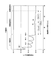
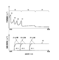
- FIG. 2A is a diagram showing an example of the distribution of impurity concentration and carrier lifetime in a part of the FS region 20 and the drift region 14.
- the horizontal axis indicates the depth from the back surface of the semiconductor substrate 10
- the vertical axis indicates the impurity concentration.
- the carrier lifetime shows a relative value that does not depend on the scale of the vertical axis.
- the peak of the impurity concentration near the depth of 0 ⁇ m corresponds to the back side region such as the cathode region.
- the back side region is formed by doping impurities such as phosphorus from the back side of the semiconductor substrate 10.
- the FS region 20 has a peak region 30 and a high concentration region 32 in order from the back side.
- the drift region 14 has a low concentration region 34 having a lower impurity concentration than the high concentration region 32.
- the entire drift region 14 may be the low concentration region 34.
- the peak region 30 is arranged on the back surface side of the center of the semiconductor substrate 10.
- the peak region 30 may be formed in a predetermined range whose distance from the back surface side of the semiconductor substrate 10 is 30 ⁇ m or less, may be formed in a predetermined range of 20 ⁇ m or less, or may be formed in a predetermined range of 10 ⁇ m or less. Good.
- the impurity concentration distribution in the peak region 30 has one or more peaks 40.
- the peak 40 is formed by doping an impurity having a small mass such as proton from the back side of the semiconductor substrate 10. By using light impurities such as protons, the position of the peak 40 can be accurately controlled.
- the impurity is preferably a substance having a lighter mass than phosphorus and selenium.
- the high concentration region 32 is arranged on the surface side of the peak region 30.
- the impurity concentration of the high concentration region 32 is higher than the impurity concentration of the semiconductor substrate 10 (in this example, the impurity concentration of the drift region 14), and the peak region 30 (peak 40 in this example) in the depth direction of the semiconductor substrate 10. Changes more slowly.
- the maximum value of the impurity concentration in the high concentration region 32 may be 1.2 times or more, 1.5 times or more, or 2 times or more of the impurity concentration in the low concentration region 34.
- the average value of the impurity concentration in the high concentration region 32 may be 1.1 times or more than the impurity concentration in the low concentration region 34, or may be 1.2 times or more.
- the impurity concentration in the low concentration region 34 described above may be an average impurity concentration in the low concentration region 34.
- the maximum value of the slope with respect to the depth of the impurity concentration distribution in the high concentration region 32 may be smaller than the average value of the slope of the impurity concentration distribution at the peak 40. Further, the maximum value of the impurity concentration in the high concentration region 32 is smaller than the maximum value of each peak 40 included in the peak region 30. Further, the maximum value of the impurity concentration in the high concentration region 32 may be smaller than the minimum value of the impurity concentration in the peak region 30.
- the high concentration region 32 may be longer than the one peak 40 in the depth direction. Further, the high concentration region 32 may be longer in the depth direction than the entire peak region 30.
- the boundary between the high concentration region 32 and the peak region 30 may be a point where the impurity concentration first shows a minimum value after the peak 40. Further, the boundary between the high concentration region 32 and the peak region 30 may be a point where the amount of change in the depth direction of the impurity concentration becomes a predetermined value or less after the peak 40. For example, a point where the change in impurity concentration is 20% or less with respect to a distance of 1 ⁇ m in the depth direction on the front surface side from the peak 40 may be the boundary on the back surface side of the high concentration region 32.
- the boundary between the high concentration region 32 and the low concentration region 34 may be a point where the impurity concentration becomes the average impurity concentration of the drift region 14.
- the high concentration region 32 is longer than the width of any peak 40.
- the width of the peak 40 refers to the width between two minimum values of the impurity concentration. Even when the peak region 30 has a plurality of peaks 40, the high concentration region 32 may be longer than the entire peak region 30.
- the low concentration region 34 is arranged on the surface side of the high concentration region 32.
- the impurity concentration of the low concentration region 34 is lower than the impurity concentration of the high concentration region 32.
- the impurity concentration in the low concentration region 34 may be the same as the impurity concentration of the semiconductor substrate 10.
- the high concentration region 32 forms a defect region extending in the depth direction in the semiconductor substrate 10 after or before doping impurities such as protons to generate the peak 40 under a predetermined condition. It is formed by heat treatment after formation.
- the defect region has a higher density of crystal defects than other regions of the semiconductor substrate 10.
- the defect region is formed in at least a part of a region where the high concentration region 32 is to be formed.
- the defect region may be formed in the same region as the region where the high concentration region 32 is to be formed, or may be formed in a region wider than the region where the high concentration region 32 is to be formed. Since there are relatively many crystal defects in the defect region, impurities such as protons are likely to diffuse to deep positions.
- the defect region can be formed by irradiating the semiconductor substrate 10 with an electron beam under predetermined conditions.
- crystal defects are formed in a region on the surface side of the peak region 30.
- impurities such as protons doped in the peak region 30 diffuse to the surface side.
- the length in the depth direction of the high concentration region 32 may be 5 ⁇ m or more.
- the length of the high concentration region 32 indicates the length from the boundary with the peak region 30 to the boundary with the low concentration region 34.
- the length of the high concentration region 32 may be 10 ⁇ m or more, 20 ⁇ m or more, or 30 ⁇ m or more.
- the length of the high concentration region 32 can be controlled by the doping amount of impurities such as protons, the range in which the defect region is formed, the density of crystal defects in the defect region, and the like.
- the length of the high concentration region 32 can be controlled by the amount of electron beam irradiation, the temperature or time of heat treatment after electron beam irradiation, and the like.
- crystal defects in the defect region formed by an electron beam or the like are recovered by diffusion of impurities such as protons, so that the carrier lifetime on the front side of the semiconductor substrate is shortened and the carrier lifetime on the back side is lengthened.
- impurities such as protons
- hydrogen is introduced into the range region of the semiconductor substrate 10 by proton injection.
- the introduced hydrogen is further diffused from the range region to the back of the semiconductor substrate 10 (in this case, the front surface side) by heat treatment.
- Hydrogen introduced in this way can terminate dangling bonds caused by point defects formed by electron beam irradiation or the like. This reduces the point defect concentration and increases the carrier lifetime. For this reason, the peak currents Irp and dv / dt during reverse recovery can be simultaneously reduced.
- the carrier lifetime in the high concentration region 32 is longer than the carrier lifetime in the low concentration region 34.
- the carrier lifetime distribution has an edge that transitions from a long lifetime to a short lifetime at the boundary between the high concentration region 32 and the low concentration region 34. Note that the carrier lifetime in the high concentration region 32 is substantially constant, and the carrier lifetime in the low concentration region 34 may gradually decrease toward the surface side.
- the peak region 30 and the high concentration region 32 include vacancies (V) introduced by proton injection or electron beam irradiation, oxygen (O) mixed during the production of the semiconductor substrate 10 or introduced during the element formation process, In addition, it is considered that a region where a donor is formed due to a vacancy-oxygen-hydrogen defect (VOH defect) due to implanted hydrogen (H).
- the donor due to the VOH defect has a donor conversion rate in the range of 0.1% to 10% with respect to the amount of hydrogen introduced or the concentration of hydrogen.
- the concentration distribution obtained by multiplying the hydrogen concentration distribution by the donor ratio is sufficiently higher than the phosphorus concentration of the semiconductor substrate 10, so that the donor concentration distribution (net doping) of the VOH defect reflecting the concentration distribution of the implanted hydrogen. Concentration distribution).
- the high concentration region 32 is a region deeper than the range Rp of the injected protons, hydrogen is a region where hydrogen has diffused from the range Rp to the back side (in this case, the front surface side) of the semiconductor substrate 10. .
- the value obtained by multiplying the diffused hydrogen concentration distribution by the donor ratio is smaller than the phosphorus concentration of the semiconductor substrate 10.
- the point defect concentration is almost uniformly distributed in a predetermined region deeper than the proton range Rp. Therefore, the diffused hydrogen concentration is combined with vacancies and oxygen to form VOH defects.
- the donor concentration as the VOH defect exceeds the phosphorus concentration of the semiconductor substrate 10, the high concentration region 32 can be formed.
- oxygen and a small amount of diffused hydrogen are combined in a substantially uniform vacancy concentration distribution, the concentration distribution of VOH defects is also substantially uniform. That is, the donor concentration distribution in the high concentration region 32 is dominated by the vacancy concentration distribution.
- the impurity concentration distribution in the high concentration region 32 has an increasing portion 42 in which the impurity concentration increases from the back surface side to the front surface side in the vicinity of the boundary with the low concentration region 34, and the increasing portion 42. It has a decreasing portion 44 which is disposed on the front surface side and the impurity concentration decreases from the back surface side to the front surface side.
- the high concentration region 32 has an impurity concentration distribution corresponding to the impurity concentration distribution in the peak region 30 because impurities such as protons doped in the peak region 30 diffuse.
- impurities such as protons doped in the peak region 30 diffuse.
- an increase portion 42 and a decrease portion 44 appear at the end of the high concentration region 32.
- the impurity concentration distribution in the high concentration region 32 becomes gentler than the impurity concentration distribution in the peak region 30.
- the absolute value of the decrease rate of the impurity concentration in the decrease portion 44 is greater than the absolute value of the increase rate of the impurity concentration in the increase portion 42. large. That is, the impurity concentration of the decrease part 44 changes more rapidly than the increase part 42.
- the distance between the peak 40 and the boundary between the increasing portion 42 and the decreasing portion 44 may be 10 ⁇ m or more, may be 20 ⁇ m or more, and may be 30 ⁇ m or more.
- the position of the peak 40 is a position of about 7 ⁇ m from the back surface of the semiconductor substrate 10
- the position of the boundary between the increasing portion 42 and the decreasing portion 44 is a position of about 40 ⁇ m from the back surface of the semiconductor substrate 10.
- FIG. 2B is a diagram for explaining a method for measuring a carrier lifetime in the semiconductor device 100.
- the defect region is formed by electron beam irradiation.
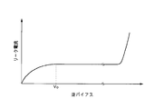
- FIG. 2B shows the relationship between the reverse bias voltage and the leakage current in the semiconductor device 100. Crystal defects are formed in the low concentration region 34 by electron beam irradiation, and the defects are not eliminated by impurities such as protons. For this reason, when the reverse bias is increased from 0 V, the leakage current gradually increases.
- the boundary position between the high concentration region 32 and the low concentration region 34 can be estimated by measuring the reverse bias voltage Vo at which the leakage current does not change. Note that the voltage Vo, the relationship between the boundary position x 0 is given by the following equation.
- FIG. 3 is a diagram showing another example of distribution of impurity concentration.
- proton is used as an impurity to be doped in the peak region 30 and electron beam irradiation is used to form a defect region.
- impurity concentration distributions 23-1, 23-2, 23-3 and 23-4 are shown for each of four types of proton doping amounts.
- the acceleration voltage for accelerating protons is 550 keV
- the annealing temperature after proton doping is 370 ° C.
- the annealing time is 5 hours
- the electron beam irradiation amount is 800 kGy
- the annealing temperature after electron beam irradiation is 360 ° C.
- the annealing time was 1 hour.
- the proton doping amount is 1.0 ⁇ 10 15 / cm 2 for distribution 23-1, 3.0 ⁇ 10 14 / cm 2 for distribution 23-2, and 1.0 ⁇ 10 14 / cm for distribution 23-3.
- cm 2 and distribution 23-4 is 1.0 ⁇ 10 13 / cm 2 .
- the higher the proton doping amount the longer the high concentration region 32 on the surface side than the peak region 30 becomes.
- the high concentration region 32 does not appear in the distribution 23-4 in which the proton doping amount is relatively small as 1.0 ⁇ 10 13 / cm 2 .
- the proton dope amount is 1.0 ⁇ 10 14 / cm 2 or more.
- the impurity concentration of the high concentration region 32 is not substantially changed. Also from this, it is preferable that the proton dope amount be 1.0 ⁇ 10 14 / cm 2 or more.
- the doping amount of protons may be greater than 3.0 ⁇ 10 14 / cm 2, may be 1.0 ⁇ 10 15 / cm 2 or more.
- FIG. 4 is a diagram showing another distribution example of the impurity concentration.
- a plurality of peaks 40 are provided in the peak region 30.
- peaks 40-1, 40-2, 40-3, 40-4 are provided in order from the back side of the peak region 30.
- the peak 40 on the most surface side may have a higher impurity concentration than the peak 40 on the back side of one of the peaks 40.
- the peak 40-4 has a higher impurity concentration than the peak 40-3.
- the peak 40-1 has a higher impurity concentration than any other peak 40.
- the peak 40-2 has a higher impurity concentration than the peak 40-3.
- the impurity concentration of the peak 40 on the most surface side may be higher than 5 ⁇ 10 14 / cm 3 . Further, the impurity concentration of the peak 40 on the most surface side may be greater than 1.2 ⁇ 10 15 / cm 3 or greater than 1.4 ⁇ 10 15 / cm 3 .
- the impurity concentration distribution of the high concentration region 32 has an increase portion 42 and a decrease portion 44.
- the peak region 30 has a plurality of peaks 40, proton diffusion in the depth direction of the high concentration region 32 is also made uniform.
- the boundary between the increasing portion 42 and the decreasing portion 44 is arranged near the center of the high concentration region 32.
- the length of the high concentration region 32 is about 43 ⁇ m, and the boundary between the increase portion 42 and the decrease portion 44 is disposed at a depth of about 21 ⁇ m to 22 ⁇ m from both ends of the high concentration region 32.
- the proton doping amount corresponding to the peak 40-1 is 3.0 ⁇ 10 14 / cm 2
- the acceleration voltage is 400 keV
- the proton doping amount corresponding to the peak 40-2 is 1.0 ⁇ 10 10. 13 / cm 2
- acceleration voltage is 820 keV
- proton doping amount corresponding to peak 40-3 is 7.0 ⁇ 10 12 / cm 2
- acceleration voltage is 1110 keV
- proton doping amount corresponding to peak 40-4 was set to 1.0 ⁇ 10 13 / cm 2 and the acceleration voltage was set to 1450 keV.
- the annealing temperature after proton doping was 370 ° C., the annealing time was 5 hours, the electron beam irradiation dose was 160 kGy, the annealing temperature after electron beam irradiation was 360 ° C., and the annealing time was 1 hour.
- FIG. 5 is a diagram showing a comparative example of the impurity concentration distribution when electron beam irradiation is performed and when it is not performed.
- the distribution 21 is a distribution under the same conditions as the distribution shown in FIG.
- the distribution 110 is a distribution when electron beam irradiation is not performed after proton annealing and annealing.
- the distribution 110 has the same conditions as the distribution 21 except that the electron beam irradiation is not performed.
- the distribution 112 is a distribution when helium is doped from the back surface of the semiconductor substrate 10 instead of performing electron beam irradiation.
- the distribution 112 has the same conditions as the distribution 21 except that helium is doped instead of electron beam irradiation.
- Helium was injected from the back surface of the semiconductor substrate 10 at a position shallower than the shallowest peak 40 when viewed from the back surface of the semiconductor substrate 10.
- helium was doped under conditions of 700 keV and 2.4 ⁇ 10 12 / cm 2 .
- the high concentration region 32 is not formed in the distribution 110 in which the electron beam irradiation is not performed and the distribution 112 in which helium doping is performed instead of the electron beam irradiation.
- the distribution 21 annealed after the electron beam irradiation a high concentration region 32 is formed.
- the high concentration region 32 can be formed by electron beam irradiation and annealing under predetermined conditions.
- the maximum value of the impurity concentration of the high concentration region 32 in the distribution 21 is 1.4 ⁇ 10 14 / cm 3 .
- the average value of the impurity concentration in the low concentration region 34 is 1.0 ⁇ 10 14 / cm 3 .
- FIG. 6 is a diagram showing an example of impurity concentration distribution when the electron beam irradiation conditions are changed.
- the distribution 23-2 is the same as the distribution 23-2 shown in FIG.
- Distribution 23-5 is an example in which the electron beam irradiation amount is changed to 800 kGy
- distribution 23-6 is an example in which the electron beam irradiation amount is changed to 1200 kGy.
- Conditions other than the electron beam irradiation amount of the distribution 23-5 and the distribution 23-6 are the same as those of the distribution 23-2.
- the electron beam irradiation dose is preferably 1500 kGy or less.
- the electron beam irradiation dose may be 1200 kGy or less, or 800 kGy or less.
- the electron beam dose is preferably 20 kGy or more.
- the electron beam dose may be adjusted according to the acceleration voltage of protons.
- FIG. 7 is a diagram illustrating an example of a method for manufacturing the semiconductor device 100.
- a base substrate is prepared, and surface structures such as the surface side region 12 and the surface side electrode 102 are formed on the surface side of the base substrate (S300).
- the semiconductor substrate 10 is formed by grinding the back side of the base substrate so as to have a substrate thickness corresponding to the breakdown voltage (S302).
- a cathode region is formed by shallowly doping impurities such as phosphorus from the back side of the semiconductor substrate 10 (S304). After doping the impurities, the cathode region is annealed with a laser or the like (S306).
- protons are doped at a position deeper than the cathode region from the back side of the semiconductor substrate 10 (S308).
- protons may be doped at one or more depth positions.
- the semiconductor substrate 10 is annealed under predetermined conditions (S310). As a result, a peak region 30 having one or more peaks 40 is formed.
- S312 and S314 may be performed between S306 and S308. That is, the electron beam irradiation may be after the proton injection or before the proton injection.
- a defect region extending in the depth direction is formed in the semiconductor substrate 10 (S312).
- a defect region may be formed by irradiating an electron beam as described above.
- the defect region is formed by extending all over the semiconductor substrate 10 in the depth direction.
- the electron beam may be irradiated from the back surface side of the semiconductor substrate 10 or from the front surface side.
- the semiconductor substrate 10 is annealed under a predetermined condition (S314). Thereby, the high concentration region 32 is formed.
- the back side electrode 104 is formed on the back side of the semiconductor substrate 10. Thereby, the semiconductor device 100 can be manufactured.
- a step of forming a floating region between S304 and S306 may be further provided.
- a predetermined mask pattern may be formed on the back side of the semiconductor substrate 10, and an impurity such as boron may be doped in a region not covered with the mask pattern.
- a step of doping helium from the back side of the semiconductor substrate 10 may be further provided between S310 and S312. In this step, helium is doped at a predetermined depth position in the peak region 30 to adjust the carrier lifetime.
- the high concentration region 32 can be formed up to a deep position of the semiconductor substrate 10. Further, the high concentration region 32 having a relatively uniform concentration can be formed. It is conceivable to form a high-concentration impurity region in a deep position of the semiconductor substrate 10 by accelerating a low-mass impurity such as proton with a high voltage. In this case, however, an expensive apparatus is required. On the other hand, according to the manufacturing method of this example, protons may be doped at a relatively shallow position, and can be realized with a simple apparatus.
- the defect region was formed by irradiating the semiconductor substrate 10 with an electron beam.
- the defect region may be formed by a method other than electron beam irradiation.
- a defect region can be formed by injecting a defect generating material into the semiconductor substrate 10.
- the crystal generation material is a material that can generate crystal defects in a region where the material passes through the semiconductor substrate 10.
- the crystal forming material is helium.
- helium doped from the back surface side of the semiconductor substrate 10 is implanted from the back surface of the semiconductor substrate 10 at a shallower range than the proton range implanted from the back surface of the semiconductor substrate 10 to the shallowest peak position. did.
- helium ions may be implanted deeper than the proton range implanted from the back surface of the semiconductor substrate 10 to the deepest peak position. Crystal defects are formed in a region through which helium ions implanted from the back surface of the semiconductor substrate 10 have passed. For this reason, the defect area
- FIG. 8 is a diagram showing an example in which helium ions are implanted deeper than the deepest proton from the back side of the semiconductor substrate 10.
- FIG. 8A is a distribution diagram showing the concentration distribution of protons (hydrogen) and the density distribution of crystal defects with respect to the depth from the implantation surface (in this example, the back surface of the semiconductor substrate 10).
- Protons may be injected at a plurality of peak positions. Protons are injected in multiple times for each peak position.
- the number of proton peak injections is 3, and the hydrogen concentration distribution in each injection is shown separately.
- Helium is injected into one injection position. Although not shown, helium may be injected into different positions a plurality of times.
- a defect region 46 extending from the back surface of the semiconductor substrate 10 is formed by passing helium.
- the defect density distribution in the defect region 46 has a peak in the vicinity of the helium implantation position. Since the defect region 46 easily diffuses protons, the protons can be diffused to the surface side of the semiconductor substrate 10 by annealing the semiconductor substrate 10 after implanting protons and helium.
- FIG. 8B is a distribution diagram showing the density distribution (left axis) of vacancies related defects and the distribution of carrier lifetime (right axis) corresponding to FIG. 8A.
- FIG. 8B shows each distribution after annealing.
- the hole-related defect density is a total density distribution of holes (V), double holes (VV), and the like.
- V holes
- VV double holes
- vacancy-related defects are most densely distributed in the vicinity of the helium range.
- FIG. 8 (c) shows the donor concentration distribution corresponding to FIGS. 8 (a) and 8 (b). Since a VOH defect can be formed in a region deeper than the deepest proton range corresponding to the hydrogen termination, a high concentration region 32 having a concentration higher than the phosphorus concentration of the semiconductor substrate 10 can be formed. Furthermore, in the proton range region where the hydrogen concentration is sufficiently high, a peak corresponding to the proton concentration distribution is formed.
- the high concentration region 32 can be formed in the same manner as the point defect formed by electron beam irradiation.
- the injection position of helium may coincide with the end position of the region where the high concentration region 32 is to be formed.
- the helium implantation position may be closer to the surface of the semiconductor substrate 10 than the end of the region where the high concentration region 32 is to be formed.
- the defect region 46 extends to the surface side of the semiconductor substrate 10 with respect to the high concentration region 32.
- FIG. 8B shows that more crystal defects remain in the region on the surface side of the semiconductor substrate 10 than in the high concentration region 32. Thereby, the carrier lifetime in the said area
- the defect region 46 may extend to the surface side of the semiconductor substrate 10 from the center in the depth direction of the semiconductor substrate 10. Further, the defect region 46 may extend to the surface side of the semiconductor substrate 10 by 40 ⁇ m or more from the impurity concentration peak 40 at the deepest position when viewed from the back surface of the semiconductor substrate 10.
- FIG. 9 is a diagram showing an example in which helium is implanted from the surface side of the semiconductor substrate 10 to form the defect region 46.
- a defect region 46 formed by extending in the depth direction from the surface of the semiconductor substrate 10 is formed in the semiconductor substrate 10.
- three types of defect regions 46 having different helium implantation positions are shown.
- the defect region 46-1 is formed in the high concentration region 32 at the tip on the back surface side of the semiconductor substrate 10. That is, a part of the defect region 46-1 is formed at the same position in the depth direction as a part of the high concentration region 32. Proton diffusion is promoted in the region where the defect region 46-1 is formed. Therefore, by forming the defect region 46-1 in at least a part of the region where the high concentration region 32 is to be formed, the high concentration region 32 can be formed in a wider range.
- the density of crystal defects before proton diffusion is shown by dotted lines.
- a peak of crystal defect density exists in the vicinity of the helium implantation position.
- crystal defects are terminated by diffusing protons by heat treatment.
- the peak of the crystal defect density can be made gentle and the leakage current can be suppressed.
- the tip of the defect region 46 may extend to the back surface side of the semiconductor substrate 10 rather than the peak 40 provided most on the front surface side of the semiconductor substrate 10 in the peak region 30. .
- region 46 can be formed over the whole area
- the tip of the defect region 46 may be formed at the same position in the depth direction as any one of the peaks 40 in the peak region 30.
- the peak of the crystal defect density in the vicinity of the helium implantation position can be made smoother. For this reason, the leakage current can be further suppressed.
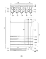
- FIG. 10A is a cross-sectional view showing an outline of a semiconductor device 200 according to the second embodiment of the present invention.
- the semiconductor substrate 10 in the semiconductor device 200 includes a transistor region 50 in which a transistor such as IGBT is formed, and a diode region 70 in which a diode such as FWD is formed.
- the transistor region 50 and the diode region 70 are adjacent to each other.
- the transistor region 50 includes, from the surface side of the semiconductor substrate 10, an N + type emitter region 58, a P type surface side region 12 that functions as a base region, an N ⁇ type drift region 14, an FS region 20, and a P + type.
- Collector region 52 is provided. Further, an N + type accumulation region 62 for improving the IE effect may be provided between the surface side region 12 and the drift region 14.
- the transistor region 50 is provided with a plurality of gate trenches 54 extending from the surface of the semiconductor substrate 10 to the drift region 14 and a plurality of emitter trenches 56.
- a gate electrode G to which a gate voltage is applied is formed inside the gate trench 54.
- an emitter electrode E that is electrically connected to the surface-side electrode 102 that functions as an emitter electrode is formed.
- An insulating film 68 is formed between the gate electrode G and the emitter electrode E and the surface side electrode 102. However, a through hole that connects the emitter electrode E and the surface-side electrode 102 is formed in a partial region of the insulating film 68.
- a P-type surface side region 12, an N ⁇ type drift region 14, an FS region 20, and an N + type cathode region 64 functioning as a base region are provided from the surface side of the semiconductor substrate 10. .
- An accumulation region 62 may also be formed in the diode region 70.
- a peak region having a plurality of peaks 40 is formed in the transistor region 50 and the FS region 20 of the diode region 70.
- the diode region 70 is provided with a plurality of emitter trenches 56 extending from the surface of the semiconductor substrate 10 to the drift region 14. Further, a back-side electrode 104 that contacts the collector region 52 and the cathode region 64 is formed on the back surface of the semiconductor substrate 10.
- the semiconductor device 200 of this example irradiates the entire semiconductor substrate 10 with an electron beam in order to form a defect region. As a result, the high concentration region 32 is formed in the transistor region 50 and the diode region 70.
- FIG. 10B is a diagram illustrating another example of the semiconductor device 200.
- FIG. 10B only the semiconductor substrate 10 is shown.
- helium ions are implanted from the back side of the semiconductor substrate 10 in order to form a defect region.
- Other structures are the same as those of the semiconductor device 200 shown in FIG. 10A.
- helium ions are implanted into the entire transistor region 50 and diode region 70.
- the helium ion implantation position 72 is closer to the surface of the semiconductor substrate 10 than the region where the high concentration region 32 is to be formed.
- a defect region 46 is formed between the back surface of the semiconductor substrate 10 and the implantation position 72. After forming the defect region 46 and injecting protons into the peak region 30, the semiconductor substrate 10 is annealed. As a result, the high concentration region 32 is formed in the transistor region 50 and the diode region 70.
- FIG. 10C is a diagram illustrating another example of the semiconductor device 200.
- FIG. 10C only the semiconductor substrate 10 is shown.
- helium ions are implanted from the back side of the semiconductor substrate 10 in order to form a defect region.
- Other structures are the same as those of the semiconductor device 200 shown in FIG. 10A.
- helium ions are implanted into the diode region 70 and helium ions are not implanted into the transistor region 50.
- a metal mask 74 that masks the transistor region 50 is used in the step of implanting helium ions.
- the helium ion implantation position 72 is closer to the surface of the semiconductor substrate 10 than the region where the high concentration region 32 is to be formed.
- a defect region 46 is formed between the back surface of the semiconductor substrate 10 and the implantation position 72. After forming the defect region 46 and injecting protons into the peak region 30, the semiconductor substrate 10 is annealed. As a result, the high concentration region 32 is formed in the diode region 70, and the high concentration region 32 is not formed in the transistor region 50.
- FIG. 10D is a diagram illustrating another example of the semiconductor device 200.
- FIG. 10D only the semiconductor substrate 10 is shown.
- helium ions are implanted from the surface side of the semiconductor substrate 10 in order to form a defect region.
- Other structures are the same as those of the semiconductor device 200 shown in FIG. 10A.
- helium ions are implanted into the entire transistor region 50 and diode region 70.
- the helium ion implantation position 72 is, for example, any position in the peak region 30.
- a defect region 46 is formed between the surface of the semiconductor substrate 10 and the implantation position 72. After forming the defect region 46 and injecting protons into the peak region 30, the semiconductor substrate 10 is annealed. As a result, the high concentration region 32 is formed in the transistor region 50 and the diode region 70.
- FIG. 10E is a diagram illustrating another example of the semiconductor device 200.
- FIG. 10E only the semiconductor substrate 10 is shown.
- helium ions are implanted from the surface side of the semiconductor substrate 10 in order to form a defect region.
- Other structures are the same as those of the semiconductor device 200 shown in FIG. 10A.
- helium ions are implanted into the diode region 70 and helium ions are not implanted into the transistor region 50.
- a metal mask 74 that masks the transistor region 50 is used in the step of implanting helium ions.
- the helium ion implantation position 72 is, for example, any position in the peak region 30.
- a defect region 46 is formed between the surface of the semiconductor substrate 10 and the implantation position 72. After forming the defect region 46 and injecting protons into the peak region 30, the semiconductor substrate 10 is annealed. As a result, the high concentration region 32 is formed in the diode region 70, and the high concentration region 32 is not formed in the transistor region 50.
- FIG. 10F is a diagram illustrating another example of the semiconductor device 200.
- the semiconductor device 200 of this example helium ions are implanted from the back side of the semiconductor substrate 10 in order to form a defect region.
- Other structures are the same as those of the semiconductor device 200 shown in FIG. 10A.
- helium ions are implanted into the diode region 70 and a part of the transistor region 50 adjacent to the diode region 70, and helium ions are implanted into a part of the transistor region 50 away from the diode region 70.
- a metal mask 74 that masks the transistor region 50 is used in the step of implanting helium ions.
- the helium ion implantation position 72 is closer to the surface of the semiconductor substrate 10 than the region where the high concentration region 32 is to be formed.
- a defect region 46 is formed between the back surface of the semiconductor substrate 10 and the implantation position 72.
- the semiconductor substrate 10 is annealed.
- the high concentration region 32 is formed in the diode region 70 and a partial region of the transistor region 50, and the high concentration region 32 is not formed in the remaining region of the transistor region 50.
- the high concentration region 32 may be formed in a partial region of the transistor region 50.
- the semiconductor substrate 10 described with reference to FIGS. 1 to 10F may be an MCZ (Magnetic Field Applied) substrate.
- the MCZ substrate has a higher oxygen concentration than the FZ substrate.
- oxygen concentration is high, VO defects are relatively increased and VV defects are relatively decreased in the semiconductor substrate 10 irradiated with the electron beam. Since VO defects are easily terminated with hydrogen, protons can be easily diffused, and the high concentration region 32 can be formed up to a deep position.
- the MCZ substrate in which protons are diffused has more VOH defects than VV defects.
- the VOH defect has a shallower level than the VV defect and hardly contributes to the leakage current. For this reason, when protons are diffused in the MCZ substrate, the leakage current can be reduced.
- FIG. 11 is a diagram showing an example of the impurity concentration distribution when the MCZ substrate is irradiated with an electron beam and when the FZ substrate is irradiated with an electron beam.
- the specific resistance of the substrate is the same between the example using the MCZ substrate and the example using the FZ substrate.
- the use of the MCZ substrate increases the impurity concentration on the surface side from the proton peak 40. For this reason, a high concentration region can be easily formed.
- the semiconductor device 100 using the MCZ substrate has a reduced leakage current as compared with the device using the FZ substrate. Further, even compared with an example in which the MCZ substrate is irradiated with an electron beam and protons are not injected, the semiconductor device 100 using the MCZ substrate has a reduced leakage current.
- the semiconductor substrate 10 may be a substrate having an average oxygen concentration of 1.0 ⁇ 10 16 / cm 3 or more and 1.0 ⁇ 10 18 / cm 3 or less. This also has the same effect as the MCZ substrate.
- the average oxygen concentration of the semiconductor substrate 10 may be 3.0 ⁇ 10 16 / cm 3 or more and 5.0 ⁇ 10 17 / cm 3 or less.
- the semiconductor substrate 10 may be a substrate having an average carbon concentration of 1.0 ⁇ 10 14 / cm 3 or more and 3.0 ⁇ 10 15 / cm 3 or less. Further, the substrate may have both the average oxygen concentration and the average carbon concentration within the above-described ranges.
- DESCRIPTION OF SYMBOLS 10 ... Semiconductor substrate, 12 ... Surface side area
Landscapes
- Metal-Oxide And Bipolar Metal-Oxide Semiconductor Integrated Circuits (AREA)
- Thin Film Transistor (AREA)
- Physics & Mathematics (AREA)
- High Energy & Nuclear Physics (AREA)
- Recrystallisation Techniques (AREA)
- Electrodes Of Semiconductors (AREA)
Abstract
Priority Applications (6)
| Application Number | Priority Date | Filing Date | Title |
|---|---|---|---|
| CN201680003833.0A CN107004723B (zh) | 2015-06-17 | 2016-06-16 | 半导体装置及半导体装置的制造方法 |
| DE112016000170.3T DE112016000170T5 (de) | 2015-06-17 | 2016-06-16 | Halbleitervorrichtung und Verfahren zur Hestellung einer Halbleitervorrichtung |
| JP2017525294A JP6311840B2 (ja) | 2015-06-17 | 2016-06-16 | 半導体装置および半導体装置の製造方法 |
| US15/607,696 US10304928B2 (en) | 2015-06-17 | 2017-05-30 | Semiconductor device and method of manufacturing semiconductor device |
| US16/358,705 US10756182B2 (en) | 2015-06-17 | 2019-03-20 | Semiconductor device and method of manufacturing semiconductor device |
| US16/997,886 US11335772B2 (en) | 2015-06-17 | 2020-08-19 | Semiconductor device and method of manufacturing semiconductor device |
Applications Claiming Priority (2)
| Application Number | Priority Date | Filing Date | Title |
|---|---|---|---|
| JP2015121751 | 2015-06-17 | ||
| JP2015-121751 | 2015-06-17 |
Related Child Applications (1)
| Application Number | Title | Priority Date | Filing Date |
|---|---|---|---|
| US15/607,696 Continuation-In-Part US10304928B2 (en) | 2015-06-17 | 2017-05-30 | Semiconductor device and method of manufacturing semiconductor device |
Publications (1)
| Publication Number | Publication Date |
|---|---|
| WO2016204227A1 true WO2016204227A1 (fr) | 2016-12-22 |
Family
ID=57545331
Family Applications (1)
| Application Number | Title | Priority Date | Filing Date |
|---|---|---|---|
| PCT/JP2016/067935 Ceased WO2016204227A1 (fr) | 2015-06-17 | 2016-06-16 | Dispositif à semi-conducteur et procédé de fabrication de dispositif à semi-conducteur |
Country Status (5)
| Country | Link |
|---|---|
| US (3) | US10304928B2 (fr) |
| JP (2) | JP6311840B2 (fr) |
| CN (1) | CN107004723B (fr) |
| DE (1) | DE112016000170T5 (fr) |
| WO (1) | WO2016204227A1 (fr) |
Cited By (20)
| Publication number | Priority date | Publication date | Assignee | Title |
|---|---|---|---|---|
| JP2018137454A (ja) * | 2015-06-17 | 2018-08-30 | 富士電機株式会社 | 半導体装置および半導体装置の製造方法 |
| JP2018157200A (ja) * | 2017-03-15 | 2018-10-04 | 富士電機株式会社 | 半導体装置 |
| WO2020080295A1 (fr) * | 2018-10-18 | 2020-04-23 | 富士電機株式会社 | Dispositif à semi-conducteur et procédé de fabrication |
| JP2021028930A (ja) * | 2019-08-09 | 2021-02-25 | 富士電機株式会社 | 半導体装置 |
| WO2021125064A1 (fr) * | 2019-12-18 | 2021-06-24 | 富士電機株式会社 | Dispositif à semi-conducteur et procédé de fabrication de dispositif à semi-conducteur |
| WO2021145397A1 (fr) * | 2020-01-17 | 2021-07-22 | 富士電機株式会社 | Dispositif semi-conducteur et procédé de fabrication de dispositif semi-conducteur |
| JPWO2021166980A1 (fr) * | 2020-02-18 | 2021-08-26 | ||
| WO2021181644A1 (fr) * | 2020-03-13 | 2021-09-16 | 三菱電機株式会社 | Dispositif à semi-conducteur et son procédé de fabrication |
| DE112020001043T5 (de) | 2019-10-11 | 2021-12-23 | Fuji Electric Co., Ltd. | Halbleitervorrichtung und herstellungsverfahren einer halbleitervorrichtung |
| JP2022097741A (ja) * | 2018-11-16 | 2022-06-30 | 富士電機株式会社 | 半導体装置および製造方法 |
| JPWO2022196768A1 (fr) * | 2021-03-17 | 2022-09-22 | ||
| JP2022161357A (ja) * | 2021-04-08 | 2022-10-21 | 富士電機株式会社 | 半導体装置および製造方法 |
| WO2023233802A1 (fr) * | 2022-05-30 | 2023-12-07 | 富士電機株式会社 | Procédé de fabrication de dispositif à semi-conducteur |
| US11972950B2 (en) | 2018-12-28 | 2024-04-30 | Fuji Electric Co., Ltd. | Semiconductor device and method for manufacturing |
| US11996452B2 (en) | 2020-01-17 | 2024-05-28 | Fuji Electric Co., Ltd. | Semiconductor device including an IGBT with reduced variation in threshold voltage |
| JPWO2024128072A1 (fr) * | 2022-12-13 | 2024-06-20 | ||
| US12051591B2 (en) | 2019-12-17 | 2024-07-30 | Fuji Electric Co., Ltd. | Semiconductor device |
| US12191358B2 (en) | 2019-08-09 | 2025-01-07 | Fuji Electric Co., Ltd. | Semiconductor device |
| US12266719B2 (en) | 2020-03-04 | 2025-04-01 | Fuji Electric Co., Ltd. | Semiconductor device, manufacturing method of semiconductor device, and power conversion device comprising semiconductor device |
| US12543355B2 (en) | 2020-11-17 | 2026-02-03 | Fuji Electric Co., Ltd. | Semiconductor device |
Families Citing this family (24)
| Publication number | Priority date | Publication date | Assignee | Title |
|---|---|---|---|---|
| JP6237921B2 (ja) * | 2014-09-30 | 2017-11-29 | 富士電機株式会社 | 半導体装置および半導体装置の製造方法 |
| JP6406452B2 (ja) * | 2015-06-30 | 2018-10-17 | 富士電機株式会社 | 半導体装置及びその製造方法 |
| JP6477897B2 (ja) * | 2015-09-16 | 2019-03-06 | 富士電機株式会社 | 半導体装置および半導体装置の製造方法 |
| JP6614326B2 (ja) * | 2016-02-15 | 2019-12-04 | 富士電機株式会社 | 半導体装置 |
| CN107924951B (zh) * | 2016-03-10 | 2021-11-23 | 富士电机株式会社 | 半导体装置 |
| JP6673501B2 (ja) * | 2016-12-08 | 2020-03-25 | 富士電機株式会社 | 半導体装置 |
| DE112018003666B4 (de) | 2017-07-19 | 2025-02-06 | Mitsubishi Electric Corporation | Verfahren zur herstellung eines halbleiterbauelements und halbleiterbauelement |
| CN109979935B (zh) * | 2017-12-28 | 2025-04-22 | 富士电机株式会社 | 半导体装置及半导体装置的制造方法 |
| DE112019000094T5 (de) * | 2018-03-19 | 2020-09-24 | Fuji Electric Co., Ltd. | Halbleitervorrichtung und verfahren zum herstellen einerhalbleitervorrichtung |
| CN119208363A (zh) | 2018-11-16 | 2024-12-27 | 富士电机株式会社 | 半导体装置及制造方法 |
| US10651281B1 (en) * | 2018-12-03 | 2020-05-12 | Globalfoundries Inc. | Substrates with self-aligned buried dielectric and polycrystalline layers |
| WO2020149354A1 (fr) * | 2019-01-18 | 2020-07-23 | 富士電機株式会社 | Dispositif semi-conducteur et procédé de fabrication de dispositif semi-conducteur |
| JP7251616B2 (ja) * | 2019-04-26 | 2023-04-04 | 富士電機株式会社 | 半導体装置および製造方法 |
| WO2021049499A1 (fr) | 2019-09-11 | 2021-03-18 | 富士電機株式会社 | Dispositif à semi-conducteur et procédé de fabrication |
| DE112020001029B4 (de) | 2019-10-11 | 2025-06-05 | Fuji Electric Co., Ltd. | Halbleitervorrichtung und herstellungsverfahren einer halbleitervorrichtung |
| JP7710830B2 (ja) * | 2020-02-18 | 2025-07-22 | 株式会社デンソー | 半導体装置 |
| JP7361634B2 (ja) * | 2020-03-02 | 2023-10-16 | 三菱電機株式会社 | 半導体装置及び半導体装置の製造方法 |
| JP7452632B2 (ja) * | 2020-04-01 | 2024-03-19 | 富士電機株式会社 | 半導体装置および半導体装置の製造方法 |
| DE112021000103T5 (de) * | 2020-04-01 | 2022-06-30 | Fuji Electric Co., Ltd. | Halbleitervorrichtung und herstellungsverfahren einer halbleitervorrichtung |
| JP7264100B2 (ja) | 2020-04-02 | 2023-04-25 | 信越半導体株式会社 | シリコン単結晶基板中のドナー濃度の制御方法 |
| DE102020110072A1 (de) * | 2020-04-09 | 2021-10-14 | Infineon Technologies Ag | Vertikale leistungs-halbleitervorrichtung und herstellungsverfahren |
| JP7515428B2 (ja) * | 2021-02-16 | 2024-07-12 | 三菱電機株式会社 | 半導体装置およびその製造方法 |
| JPWO2024100926A1 (fr) * | 2022-11-08 | 2024-05-16 | ||
| JP2025050265A (ja) * | 2023-09-22 | 2025-04-04 | 株式会社東芝 | 半導体装置の製造方法、および半導体装置 |
Citations (5)
| Publication number | Priority date | Publication date | Assignee | Title |
|---|---|---|---|---|
| JP2006344823A (ja) * | 2005-06-09 | 2006-12-21 | Sumco Corp | Igbt用のシリコンウェーハ及びその製造方法 |
| WO2011125156A1 (fr) * | 2010-04-02 | 2011-10-13 | トヨタ自動車株式会社 | Dispositif à semi-conducteurs pourvu d'un substrat semi-conducteur comportant une région de diode et une région de composant igbt |
| JP2012069861A (ja) * | 2010-09-27 | 2012-04-05 | Renesas Electronics Corp | 半導体装置の製造方法 |
| JP2013138172A (ja) * | 2011-11-30 | 2013-07-11 | Denso Corp | 半導体装置 |
| WO2013141221A1 (fr) * | 2012-03-19 | 2013-09-26 | 富士電機株式会社 | Procédé de production d'un dispositif semi-conducteur |
Family Cites Families (54)
| Publication number | Priority date | Publication date | Assignee | Title |
|---|---|---|---|---|
| JPS55128869A (en) * | 1979-03-26 | 1980-10-06 | Mitsubishi Electric Corp | Semiconductor device and method of fabricating the same |
| US5528058A (en) * | 1986-03-21 | 1996-06-18 | Advanced Power Technology, Inc. | IGBT device with platinum lifetime control and reduced gaw |
| JP2984478B2 (ja) * | 1992-08-15 | 1999-11-29 | 株式会社東芝 | 伝導度変調型半導体装置及びその製造方法 |
| KR100213201B1 (ko) * | 1996-05-15 | 1999-08-02 | 윤종용 | 씨모스 트랜지스터 및 그 제조방법 |
| TW389995B (en) * | 1998-06-03 | 2000-05-11 | United Microelectronics Corp | Method of manufacturing high-voltage metal-oxide-semiconductor device |
| JP2000091443A (ja) * | 1998-09-14 | 2000-03-31 | Mitsubishi Electric Corp | 半導体装置およびその製造方法 |
| JP3416537B2 (ja) * | 1998-11-13 | 2003-06-16 | 富士通カンタムデバイス株式会社 | 化合物半導体装置及びその製造方法 |
| KR100401130B1 (ko) * | 2001-03-28 | 2003-10-10 | 한국전자통신연구원 | 수직형 채널을 가지는 초미세 mos 트랜지스터 제조방법 |
| KR100954332B1 (ko) * | 2003-06-30 | 2010-04-21 | 엘지디스플레이 주식회사 | 액정표시소자와 그 제조방법 |
| KR100598035B1 (ko) * | 2004-02-24 | 2006-07-07 | 삼성전자주식회사 | 전하 전송 이미지 소자의 제조 방법 |
| JP2005322712A (ja) | 2004-05-07 | 2005-11-17 | Toyota Motor Corp | 半導体基板,半導体装置,およびそれらの製造方法 |
| KR100599595B1 (ko) * | 2004-05-24 | 2006-07-13 | 삼성에스디아이 주식회사 | 발광표시 장치용 반도체 소자 및 그 제조 방법 |
| DE102004047749B4 (de) * | 2004-09-30 | 2008-12-04 | Infineon Technologies Austria Ag | Halbleiterbauteil Diode und IGBT sowie dafür geeignetes Herstellungsverfahren |
| DE102005026408B3 (de) * | 2005-06-08 | 2007-02-01 | Infineon Technologies Ag | Verfahren zur Herstellung einer Stoppzone in einem Halbleiterkörper und Halbleiterbauelement mit einer Stoppzone |
| US7554137B2 (en) * | 2005-10-25 | 2009-06-30 | Infineon Technologies Austria Ag | Power semiconductor component with charge compensation structure and method for the fabrication thereof |
| JP5151975B2 (ja) * | 2006-02-24 | 2013-02-27 | 三菱電機株式会社 | 半導体装置の製造方法 |
| JP5111867B2 (ja) * | 2007-01-16 | 2013-01-09 | 株式会社ジャパンディスプレイイースト | 表示装置 |
| JP5203667B2 (ja) | 2007-10-16 | 2013-06-05 | トヨタ自動車株式会社 | 半導体装置の製造方法 |
| JP5365009B2 (ja) | 2008-01-23 | 2013-12-11 | 富士電機株式会社 | 半導体装置およびその製造方法 |
| DE102008049664B3 (de) * | 2008-09-30 | 2010-02-11 | Infineon Technologies Austria Ag | Verfahren zum Herstellen eines Halbleiterkörpers mit einem graduellen pn-Übergang |
| WO2010057978A1 (fr) * | 2008-11-20 | 2010-05-27 | Saphire Aps | Tranche à base de semi-conducteurs haute tension et module solaire à dispositifs électroniques intégrés |
| WO2013031212A1 (fr) * | 2011-08-29 | 2013-03-07 | 次世代パワーデバイス技術研究組合 | Elément bidirectionnel, circuit d'élément bidirectionnel et appareil de conversion de puissance |
| DE102011113549B4 (de) | 2011-09-15 | 2019-10-17 | Infineon Technologies Ag | Ein Halbleiterbauelement mit einer Feldstoppzone in einem Halbleiterkörper und ein Verfahren zur Herstellung einer Feldstoppzone in einem Halbleiterkörper |
| JP2013074181A (ja) * | 2011-09-28 | 2013-04-22 | Toyota Motor Corp | 半導体装置とその製造方法 |
| WO2013089256A1 (fr) * | 2011-12-15 | 2013-06-20 | 富士電機株式会社 | Dispositif semi-conducteur et procédé de fabrication d'un dispositif semi-conducteur |
| JP6067585B2 (ja) | 2011-12-28 | 2017-01-25 | 富士電機株式会社 | 半導体装置および半導体装置の製造方法 |
| CN104303285B (zh) * | 2012-08-22 | 2017-03-01 | 富士电机株式会社 | 半导体装置以及半导体装置的制造方法 |
| CN104620391B (zh) * | 2012-10-23 | 2017-09-19 | 富士电机株式会社 | 半导体装置及其制造方法 |
| US9590083B2 (en) * | 2012-12-06 | 2017-03-07 | Institute of Microelectronics, Chinese Academy of Sciences | ITC-IGBT and manufacturing method therefor |
| JP6144510B2 (ja) * | 2013-03-11 | 2017-06-07 | 三菱電機株式会社 | 半導体装置の製造方法 |
| CN103178006B (zh) * | 2013-03-29 | 2015-09-23 | 上海和辉光电有限公司 | 调整低温多晶硅晶体管阀值电压的方法 |
| JP6037012B2 (ja) | 2013-06-26 | 2016-11-30 | 富士電機株式会社 | 半導体装置および半導体装置の製造方法 |
| US9166027B2 (en) * | 2013-09-30 | 2015-10-20 | Infineon Technologies Ag | IGBT with reduced feedback capacitance |
| US9012980B1 (en) * | 2013-12-04 | 2015-04-21 | Infineon Technologies Ag | Method of manufacturing a semiconductor device including proton irradiation and semiconductor device including charge compensation structure |
| US9484221B2 (en) * | 2014-01-13 | 2016-11-01 | Infineon Technologies Ag | Bipolar semiconductor device and method of manufacturing thereof |
| US10211325B2 (en) * | 2014-01-28 | 2019-02-19 | Infineon Technologies Ag | Semiconductor device including undulated profile of net doping in a drift zone |
| US9312135B2 (en) | 2014-03-19 | 2016-04-12 | Infineon Technologies Ag | Method of manufacturing semiconductor devices including generating and annealing radiation-induced crystal defects |
| JP6332446B2 (ja) * | 2014-06-12 | 2018-05-30 | 富士電機株式会社 | 半導体装置 |
| US9754787B2 (en) | 2014-06-24 | 2017-09-05 | Infineon Technologies Ag | Method for treating a semiconductor wafer |
| CN105814694B (zh) * | 2014-10-03 | 2019-03-08 | 富士电机株式会社 | 半导体装置以及半导体装置的制造方法 |
| DE102014117538A1 (de) | 2014-11-28 | 2016-06-02 | Infineon Technologies Ag | Verfahren zum Herstellen von Halbleitervorrichtungen unter Verwendung von Implantation leichter Ionen und Halbleitervorrichtung |
| KR101955055B1 (ko) * | 2014-11-28 | 2019-03-07 | 매그나칩 반도체 유한회사 | 전력용 반도체 소자 및 그 소자의 제조 방법 |
| DE102014119088A1 (de) * | 2014-12-18 | 2016-06-23 | Infineon Technologies Ag | Ein Verfahren zum Bilden eines Halbleiterbauelements und eines Halbleitersubstrats |
| DE102015107085B4 (de) | 2015-05-06 | 2025-04-10 | Infineon Technologies Ag | Verfahren zum Herstellen von Halbleitervorrichtungen und sauerstoffkorrelierte thermische Donatoren enthaltende Halbleitervorrichtung |
| WO2016204227A1 (fr) * | 2015-06-17 | 2016-12-22 | 富士電機株式会社 | Dispositif à semi-conducteur et procédé de fabrication de dispositif à semi-conducteur |
| JP6733739B2 (ja) * | 2016-10-17 | 2020-08-05 | 富士電機株式会社 | 半導体装置 |
| DE102016120771B3 (de) | 2016-10-31 | 2018-03-08 | Infineon Technologies Ag | Verfahren zum Herstellen von Halbleitervorrichtungen und Halbleitervorrichtung, die wasserstoff-korrelierte Donatoren enthält |
| WO2018092788A1 (fr) * | 2016-11-16 | 2018-05-24 | 富士電機株式会社 | Dispositif à semiconducteur |
| DE102017127169B4 (de) * | 2017-11-17 | 2022-01-27 | Infineon Technologies Ag | Verfahren zur herstellung eines halbleiterbauelements |
| JP7052322B2 (ja) * | 2017-11-28 | 2022-04-12 | 富士電機株式会社 | 炭化珪素半導体装置および炭化珪素半導体装置の製造方法 |
| DE112019000094T5 (de) * | 2018-03-19 | 2020-09-24 | Fuji Electric Co., Ltd. | Halbleitervorrichtung und verfahren zum herstellen einerhalbleitervorrichtung |
| JP7173312B2 (ja) * | 2019-05-16 | 2022-11-16 | 富士電機株式会社 | 半導体装置および半導体装置の製造方法 |
| WO2021029285A1 (fr) * | 2019-08-09 | 2021-02-18 | 富士電機株式会社 | Dispositif à semi-conducteur |
| US11996452B2 (en) * | 2020-01-17 | 2024-05-28 | Fuji Electric Co., Ltd. | Semiconductor device including an IGBT with reduced variation in threshold voltage |
-
2016
- 2016-06-16 WO PCT/JP2016/067935 patent/WO2016204227A1/fr not_active Ceased
- 2016-06-16 DE DE112016000170.3T patent/DE112016000170T5/de active Pending
- 2016-06-16 JP JP2017525294A patent/JP6311840B2/ja active Active
- 2016-06-16 CN CN201680003833.0A patent/CN107004723B/zh active Active
-
2017
- 2017-05-30 US US15/607,696 patent/US10304928B2/en active Active
-
2018
- 2018-03-20 JP JP2018053576A patent/JP6642609B2/ja active Active
-
2019
- 2019-03-20 US US16/358,705 patent/US10756182B2/en active Active
-
2020
- 2020-08-19 US US16/997,886 patent/US11335772B2/en active Active
Patent Citations (5)
| Publication number | Priority date | Publication date | Assignee | Title |
|---|---|---|---|---|
| JP2006344823A (ja) * | 2005-06-09 | 2006-12-21 | Sumco Corp | Igbt用のシリコンウェーハ及びその製造方法 |
| WO2011125156A1 (fr) * | 2010-04-02 | 2011-10-13 | トヨタ自動車株式会社 | Dispositif à semi-conducteurs pourvu d'un substrat semi-conducteur comportant une région de diode et une région de composant igbt |
| JP2012069861A (ja) * | 2010-09-27 | 2012-04-05 | Renesas Electronics Corp | 半導体装置の製造方法 |
| JP2013138172A (ja) * | 2011-11-30 | 2013-07-11 | Denso Corp | 半導体装置 |
| WO2013141221A1 (fr) * | 2012-03-19 | 2013-09-26 | 富士電機株式会社 | Procédé de production d'un dispositif semi-conducteur |
Cited By (58)
| Publication number | Priority date | Publication date | Assignee | Title |
|---|---|---|---|---|
| JP2018137454A (ja) * | 2015-06-17 | 2018-08-30 | 富士電機株式会社 | 半導体装置および半導体装置の製造方法 |
| US11335772B2 (en) | 2015-06-17 | 2022-05-17 | Fuji Electric Co., Ltd. | Semiconductor device and method of manufacturing semiconductor device |
| US10756182B2 (en) | 2015-06-17 | 2020-08-25 | Fuji Electric Co., Ltd. | Semiconductor device and method of manufacturing semiconductor device |
| JP2018157200A (ja) * | 2017-03-15 | 2018-10-04 | 富士電機株式会社 | 半導体装置 |
| JP7020185B2 (ja) | 2017-03-15 | 2022-02-16 | 富士電機株式会社 | 半導体装置 |
| DE112019008041B4 (de) * | 2018-10-18 | 2026-02-05 | Fuji Electric Co., Ltd. | Halbleitervorrichtung und herstellungsverfahren davon |
| US12191148B2 (en) | 2018-10-18 | 2025-01-07 | Fuji Electric Co., Ltd. | Semiconductor device and manufacturing method thereof |
| US11735424B2 (en) | 2018-10-18 | 2023-08-22 | Fuji Electric Co., Ltd. | Semiconductor device and manufacturing method thereof |
| WO2020080295A1 (fr) * | 2018-10-18 | 2020-04-23 | 富士電機株式会社 | Dispositif à semi-conducteur et procédé de fabrication |
| US11342186B2 (en) | 2018-10-18 | 2022-05-24 | Fuji Electric Co., Ltd. | Semiconductor device and manufacturing method thereof |
| US12266532B2 (en) | 2018-11-16 | 2025-04-01 | Fuji Electric Co., Ltd. | Semiconductor device and fabrication method |
| US11854782B2 (en) | 2018-11-16 | 2023-12-26 | Fuji Electric Co., Ltd. | Semiconductor device and fabrication method |
| JP7400874B2 (ja) | 2018-11-16 | 2023-12-19 | 富士電機株式会社 | 半導体装置および製造方法 |
| JP2022097741A (ja) * | 2018-11-16 | 2022-06-30 | 富士電機株式会社 | 半導体装置および製造方法 |
| US12368048B2 (en) | 2018-12-28 | 2025-07-22 | Fuji Electric Co., Ltd. | Semiconductor device and method for manufacturing |
| JP2024175139A (ja) * | 2018-12-28 | 2024-12-17 | 富士電機株式会社 | 半導体装置 |
| US11972950B2 (en) | 2018-12-28 | 2024-04-30 | Fuji Electric Co., Ltd. | Semiconductor device and method for manufacturing |
| JP7790508B2 (ja) | 2018-12-28 | 2025-12-23 | 富士電機株式会社 | 半導体装置 |
| JP7404702B2 (ja) | 2019-08-09 | 2023-12-26 | 富士電機株式会社 | 半導体装置 |
| US12191358B2 (en) | 2019-08-09 | 2025-01-07 | Fuji Electric Co., Ltd. | Semiconductor device |
| JP2021028930A (ja) * | 2019-08-09 | 2021-02-25 | 富士電機株式会社 | 半導体装置 |
| US12261058B2 (en) | 2019-10-11 | 2025-03-25 | Fuji Electric Co., Ltd. | Semiconductor device and manufacturing method of semiconductor device |
| DE112020001043T5 (de) | 2019-10-11 | 2021-12-23 | Fuji Electric Co., Ltd. | Halbleitervorrichtung und herstellungsverfahren einer halbleitervorrichtung |
| US12051591B2 (en) | 2019-12-17 | 2024-07-30 | Fuji Electric Co., Ltd. | Semiconductor device |
| JP7823694B2 (ja) | 2019-12-18 | 2026-03-04 | 富士電機株式会社 | 半導体装置および半導体装置の製造方法 |
| JP7215599B2 (ja) | 2019-12-18 | 2023-01-31 | 富士電機株式会社 | 半導体装置および半導体装置の製造方法 |
| US12119227B2 (en) | 2019-12-18 | 2024-10-15 | Fuji Electric Co., Ltd. | Semiconductor apparatus and manufacturing method of semiconductor apparatus |
| WO2021125064A1 (fr) * | 2019-12-18 | 2021-06-24 | 富士電機株式会社 | Dispositif à semi-conducteur et procédé de fabrication de dispositif à semi-conducteur |
| JPWO2021125064A1 (fr) * | 2019-12-18 | 2021-06-24 | ||
| JP2024157038A (ja) * | 2019-12-18 | 2024-11-06 | 富士電機株式会社 | 半導体装置および半導体装置の製造方法 |
| WO2021145397A1 (fr) * | 2020-01-17 | 2021-07-22 | 富士電機株式会社 | Dispositif semi-conducteur et procédé de fabrication de dispositif semi-conducteur |
| JPWO2021145397A1 (fr) * | 2020-01-17 | 2021-07-22 | ||
| US12294025B2 (en) | 2020-01-17 | 2025-05-06 | Fuji Electric Co., Ltd. | Semiconductor apparatus and manufacturing method of semiconductor apparatus |
| US11996452B2 (en) | 2020-01-17 | 2024-05-28 | Fuji Electric Co., Ltd. | Semiconductor device including an IGBT with reduced variation in threshold voltage |
| JP7231066B2 (ja) | 2020-01-17 | 2023-03-01 | 富士電機株式会社 | 半導体装置および半導体装置の製造方法 |
| US12087827B2 (en) | 2020-02-18 | 2024-09-10 | Fuji Electric Co., Ltd. | Semiconductor device |
| JPWO2021166980A1 (fr) * | 2020-02-18 | 2021-08-26 | ||
| JP7279846B2 (ja) | 2020-02-18 | 2023-05-23 | 富士電機株式会社 | 半導体装置 |
| CN114175270A (zh) * | 2020-02-18 | 2022-03-11 | 富士电机株式会社 | 半导体装置 |
| US12266719B2 (en) | 2020-03-04 | 2025-04-01 | Fuji Electric Co., Ltd. | Semiconductor device, manufacturing method of semiconductor device, and power conversion device comprising semiconductor device |
| US12354878B2 (en) | 2020-03-13 | 2025-07-08 | Mitsubishi Electric Corporation | Semiconductor device having semiconductor substrate including hydrogen-related donor, and manufacturing method therefor |
| JP6976493B1 (ja) * | 2020-03-13 | 2021-12-08 | 三菱電機株式会社 | 半導体装置およびその製造方法 |
| WO2021181644A1 (fr) * | 2020-03-13 | 2021-09-16 | 三菱電機株式会社 | Dispositif à semi-conducteur et son procédé de fabrication |
| US12543355B2 (en) | 2020-11-17 | 2026-02-03 | Fuji Electric Co., Ltd. | Semiconductor device |
| JP7473075B2 (ja) | 2021-03-17 | 2024-04-23 | 富士電機株式会社 | 半導体装置 |
| US12593478B2 (en) | 2021-03-17 | 2026-03-31 | Fuji Electric Co., Ltd. | Semiconductor device |
| CN115989563A (zh) * | 2021-03-17 | 2023-04-18 | 富士电机株式会社 | 半导体装置 |
| WO2022196768A1 (fr) * | 2021-03-17 | 2022-09-22 | 富士電機株式会社 | Dispositif semi-conducteur |
| JPWO2022196768A1 (fr) * | 2021-03-17 | 2022-09-22 | ||
| JP7683287B2 (ja) | 2021-04-08 | 2025-05-27 | 富士電機株式会社 | 半導体装置および製造方法 |
| US12557573B2 (en) | 2021-04-08 | 2026-02-17 | Fuji Electric Co., Ltd. | Semiconductor device provided with at least IGBT |
| JP2022161357A (ja) * | 2021-04-08 | 2022-10-21 | 富士電機株式会社 | 半導体装置および製造方法 |
| WO2023233802A1 (fr) * | 2022-05-30 | 2023-12-07 | 富士電機株式会社 | Procédé de fabrication de dispositif à semi-conducteur |
| JPWO2023233802A1 (fr) * | 2022-05-30 | 2023-12-07 | ||
| JP7652341B2 (ja) | 2022-05-30 | 2025-03-27 | 富士電機株式会社 | 半導体装置の製造方法 |
| WO2024128072A1 (fr) * | 2022-12-13 | 2024-06-20 | 富士電機株式会社 | Dispositif à semi-conducteur et procédé de fabrication de dispositif à semi-conducteur |
| JP7831641B2 (ja) | 2022-12-13 | 2026-03-17 | 富士電機株式会社 | 半導体装置および半導体装置の製造方法 |
| JPWO2024128072A1 (fr) * | 2022-12-13 | 2024-06-20 |
Also Published As
| Publication number | Publication date |
|---|---|
| US20200381515A1 (en) | 2020-12-03 |
| US20170271447A1 (en) | 2017-09-21 |
| US10304928B2 (en) | 2019-05-28 |
| JP6642609B2 (ja) | 2020-02-05 |
| JPWO2016204227A1 (ja) | 2017-09-28 |
| US10756182B2 (en) | 2020-08-25 |
| DE112016000170T5 (de) | 2017-08-03 |
| US11335772B2 (en) | 2022-05-17 |
| JP6311840B2 (ja) | 2018-04-18 |
| US20190214462A1 (en) | 2019-07-11 |
| JP2018137454A (ja) | 2018-08-30 |
| CN107004723A (zh) | 2017-08-01 |
| CN107004723B (zh) | 2021-03-09 |
Similar Documents
| Publication | Publication Date | Title |
|---|---|---|
| JP6311840B2 (ja) | 半導体装置および半導体装置の製造方法 | |
| JP6428945B2 (ja) | 半導体装置および半導体装置の製造方法 | |
| JP6508372B2 (ja) | 半導体装置および半導体装置の製造方法 | |
| US10056451B2 (en) | Semiconductor device and method for producing semiconductor device | |
| JP6708266B2 (ja) | 半導体装置 | |
| US9530672B2 (en) | Production method for a semiconductor device | |
| US9887190B2 (en) | Semiconductor device and method for manufacturing the same | |
| JP2013074181A (ja) | 半導体装置とその製造方法 | |
| CN104282759A (zh) | 超结mosfet及其制造方法和复合半导体装置 | |
| JP5261324B2 (ja) | 半導体装置とその製造方法 | |
| TWI553714B (zh) | 半導體裝置之製造方法 | |
| JP5272299B2 (ja) | 半導体装置およびその製造方法 | |
| JP6365790B2 (ja) | 半導体装置および半導体装置の製造方法 | |
| JP2010114368A (ja) | 半導体装置とその製造方法 | |
| CN116264250A (zh) | 半导体装置以及半导体装置的制造方法 | |
| DE102021127927A1 (de) | Verfahren zum herstellen einer halbleitervorrichtung einschliesslich einer ionenimplantation und halbleitervorrichtung | |
| JP2008135439A (ja) | バイポーラ半導体装置とその製造方法 |
Legal Events
| Date | Code | Title | Description |
|---|---|---|---|
| 121 | Ep: the epo has been informed by wipo that ep was designated in this application |
Ref document number: 16811701 Country of ref document: EP Kind code of ref document: A1 |
|
| ENP | Entry into the national phase |
Ref document number: 2017525294 Country of ref document: JP Kind code of ref document: A |
|
| WWE | Wipo information: entry into national phase |
Ref document number: 112016000170 Country of ref document: DE |
|
| 122 | Ep: pct application non-entry in european phase |
Ref document number: 16811701 Country of ref document: EP Kind code of ref document: A1 |