WO2017191815A1 - 仮固定用樹脂フィルム - Google Patents
仮固定用樹脂フィルム Download PDFInfo
- Publication number
- WO2017191815A1 WO2017191815A1 PCT/JP2017/016978 JP2017016978W WO2017191815A1 WO 2017191815 A1 WO2017191815 A1 WO 2017191815A1 JP 2017016978 W JP2017016978 W JP 2017016978W WO 2017191815 A1 WO2017191815 A1 WO 2017191815A1
- Authority
- WO
- WIPO (PCT)
- Prior art keywords
- layer
- resin
- film
- resin film
- electronic component
- Prior art date
- Legal status (The legal status is an assumption and is not a legal conclusion. Google has not performed a legal analysis and makes no representation as to the accuracy of the status listed.)
- Ceased
Links
Images


Classifications
-
- C—CHEMISTRY; METALLURGY
- C09—DYES; PAINTS; POLISHES; NATURAL RESINS; ADHESIVES; COMPOSITIONS NOT OTHERWISE PROVIDED FOR; APPLICATIONS OF MATERIALS NOT OTHERWISE PROVIDED FOR
- C09J—ADHESIVES; NON-MECHANICAL ASPECTS OF ADHESIVE PROCESSES IN GENERAL; ADHESIVE PROCESSES NOT PROVIDED FOR ELSEWHERE; USE OF MATERIALS AS ADHESIVES
- C09J7/00—Adhesives in the form of films or foils
- C09J7/20—Adhesives in the form of films or foils characterised by their carriers
- C09J7/29—Laminated material
-
- B—PERFORMING OPERATIONS; TRANSPORTING
- B32—LAYERED PRODUCTS
- B32B—LAYERED PRODUCTS, i.e. PRODUCTS BUILT-UP OF STRATA OF FLAT OR NON-FLAT, e.g. CELLULAR OR HONEYCOMB, FORM
- B32B27/00—Layered products comprising a layer of synthetic resin
-
- C—CHEMISTRY; METALLURGY
- C09—DYES; PAINTS; POLISHES; NATURAL RESINS; ADHESIVES; COMPOSITIONS NOT OTHERWISE PROVIDED FOR; APPLICATIONS OF MATERIALS NOT OTHERWISE PROVIDED FOR
- C09J—ADHESIVES; NON-MECHANICAL ASPECTS OF ADHESIVE PROCESSES IN GENERAL; ADHESIVE PROCESSES NOT PROVIDED FOR ELSEWHERE; USE OF MATERIALS AS ADHESIVES
- C09J7/00—Adhesives in the form of films or foils
- C09J7/10—Adhesives in the form of films or foils without carriers
-
- B—PERFORMING OPERATIONS; TRANSPORTING
- B32—LAYERED PRODUCTS
- B32B—LAYERED PRODUCTS, i.e. PRODUCTS BUILT-UP OF STRATA OF FLAT OR NON-FLAT, e.g. CELLULAR OR HONEYCOMB, FORM
- B32B27/00—Layered products comprising a layer of synthetic resin
- B32B27/06—Layered products comprising a layer of synthetic resin as the main or only constituent of a layer, which is next to another layer of the same or of a different material
- B32B27/08—Layered products comprising a layer of synthetic resin as the main or only constituent of a layer, which is next to another layer of the same or of a different material of synthetic resin
-
- C—CHEMISTRY; METALLURGY
- C09—DYES; PAINTS; POLISHES; NATURAL RESINS; ADHESIVES; COMPOSITIONS NOT OTHERWISE PROVIDED FOR; APPLICATIONS OF MATERIALS NOT OTHERWISE PROVIDED FOR
- C09J—ADHESIVES; NON-MECHANICAL ASPECTS OF ADHESIVE PROCESSES IN GENERAL; ADHESIVE PROCESSES NOT PROVIDED FOR ELSEWHERE; USE OF MATERIALS AS ADHESIVES
- C09J11/00—Features of adhesives not provided for in group C09J9/00, e.g. additives
- C09J11/02—Non-macromolecular additives
- C09J11/06—Non-macromolecular additives organic
-
- C—CHEMISTRY; METALLURGY
- C09—DYES; PAINTS; POLISHES; NATURAL RESINS; ADHESIVES; COMPOSITIONS NOT OTHERWISE PROVIDED FOR; APPLICATIONS OF MATERIALS NOT OTHERWISE PROVIDED FOR
- C09J—ADHESIVES; NON-MECHANICAL ASPECTS OF ADHESIVE PROCESSES IN GENERAL; ADHESIVE PROCESSES NOT PROVIDED FOR ELSEWHERE; USE OF MATERIALS AS ADHESIVES
- C09J183/00—Adhesives based on macromolecular compounds obtained by reactions forming in the main chain of the macromolecule a linkage containing silicon, with or without sulfur, nitrogen, oxygen, or carbon only; Adhesives based on derivatives of such polymers
- C09J183/04—Polysiloxanes
-
- C—CHEMISTRY; METALLURGY
- C09—DYES; PAINTS; POLISHES; NATURAL RESINS; ADHESIVES; COMPOSITIONS NOT OTHERWISE PROVIDED FOR; APPLICATIONS OF MATERIALS NOT OTHERWISE PROVIDED FOR
- C09J—ADHESIVES; NON-MECHANICAL ASPECTS OF ADHESIVE PROCESSES IN GENERAL; ADHESIVE PROCESSES NOT PROVIDED FOR ELSEWHERE; USE OF MATERIALS AS ADHESIVES
- C09J201/00—Adhesives based on unspecified macromolecular compounds
-
- C—CHEMISTRY; METALLURGY
- C09—DYES; PAINTS; POLISHES; NATURAL RESINS; ADHESIVES; COMPOSITIONS NOT OTHERWISE PROVIDED FOR; APPLICATIONS OF MATERIALS NOT OTHERWISE PROVIDED FOR
- C09J—ADHESIVES; NON-MECHANICAL ASPECTS OF ADHESIVE PROCESSES IN GENERAL; ADHESIVE PROCESSES NOT PROVIDED FOR ELSEWHERE; USE OF MATERIALS AS ADHESIVES
- C09J201/00—Adhesives based on unspecified macromolecular compounds
- C09J201/02—Adhesives based on unspecified macromolecular compounds characterised by the presence of specified groups, e.g. terminal or pendant functional groups
-
- C—CHEMISTRY; METALLURGY
- C09—DYES; PAINTS; POLISHES; NATURAL RESINS; ADHESIVES; COMPOSITIONS NOT OTHERWISE PROVIDED FOR; APPLICATIONS OF MATERIALS NOT OTHERWISE PROVIDED FOR
- C09J—ADHESIVES; NON-MECHANICAL ASPECTS OF ADHESIVE PROCESSES IN GENERAL; ADHESIVE PROCESSES NOT PROVIDED FOR ELSEWHERE; USE OF MATERIALS AS ADHESIVES
- C09J2301/00—Additional features of adhesives in the form of films or foils
- C09J2301/20—Additional features of adhesives in the form of films or foils characterized by the structural features of the adhesive itself
- C09J2301/208—Additional features of adhesives in the form of films or foils characterized by the structural features of the adhesive itself the adhesive layer being constituted by at least two or more adjacent or superposed adhesive layers, e.g. multilayer adhesive
Definitions
- the present invention relates to a resin film for temporary fixing.
- a support tape called a BG tape
- the thinned semiconductor element tends to warp due to the influence of the circuit applied to the surface.
- the BG tape which is a tape material that is easily deformed, is becoming unable to sufficiently support a thinned semiconductor element.
- the productivity tends to decrease.
- the method of reducing the adhesiveness by heating is concerned about the influence on the semiconductor element due to heating and is inferior in heat resistance, and therefore cannot be used in a process application for forming a through electrode or the like.
- introduction of expensive laser equipment is indispensable, and considerable investment is indispensable for application of such a process.
- the electronic parts to be processed are not limited to those having high smoothness, and there is an increasing tendency to process a wafer having a solder ball on the circuit surface and surface irregularities exceeding 80 ⁇ m. In the case of such a large uneven surface, if the unevenness is sufficiently embedded, it becomes difficult to peel the adhesive from the surface. Further, when the adhesive strength of the solder balls is insufficient, there is a concern that the solder balls are lost when the pressure-sensitive adhesive is peeled off.
- the present invention has been made in view of the above circumstances, and provides a temporary fixing resin film that can satisfactorily process an electronic component and can be easily peeled off from the processed electronic component and a support.
- the purpose is to do.
- the present invention includes a first layer containing a first thermoplastic resin having a glass transition temperature of ⁇ 50 ° C. to 50 ° C., a second thermoplastic resin having a glass transition temperature of ⁇ 50 ° C. to 50 ° C., and curing And a second layer containing a sex component.
- the electronic component can be satisfactorily processed by having the first and second layers, and from the processed electronic component and the support. It can be easily peeled off. That is, by providing the resin film with two layers, the peel strength with respect to the electronic component surface and the peel strength with respect to the support surface can be adjusted, respectively, and damage to the electronic component or breakage of the adhesive can be prevented. Moreover, the physical property (for example, shear viscosity) required at the time of processing and the peelability from a support body can be reconciled by sticking the 2nd layer which has the said specific composition on a support body surface.
- the film thickness can be easily controlled, and variations in thickness between individual electronic components can be reduced.
- the resin film for temporary fixing which concerns on this invention can be bonded together on an electronic component or a support body by simple methods, such as a lamination, and is excellent also in workability
- the content of the curable component in the second layer may be 10 to 500 parts by mass with respect to 100 parts by mass of the second thermoplastic resin. If content of the sclerosing
- the temporary fixing resin film according to the present invention may have a first layer thickness of 10 to 350 ⁇ m and a second layer thickness of 10 to 350 ⁇ m. If the thickness of the resin film for temporary fixing is within the above range, it is easy to sufficiently bury the surface unevenness of the electronic component such as a semiconductor element, and the electronic component and the support can be more reliably fixed. it can.
- the thickness of the first layer and the thickness of the second layer may satisfy the relationship of the following formula (1).
- a represents the thickness of a 1st layer
- b represents the thickness of a 2nd layer.
- the thickness ratio is within the above range, it is possible to easily adjust the peel strength of the electronic component surface and the peel strength of the pressure sensitive adhesive support surface.
- the first thermoplastic resin and / or the second thermoplastic resin has a crosslinkable functional group and has a weight average molecular weight of 100,000 to 1,200,000. Resin may be used. In this case, the first layer and the second layer can exhibit better peelability.
- the curable component may be a thermosetting resin.
- the first layer and / or the second layer may further contain a silicone compound.
- the first layer and / or the second layer may further contain a curing accelerator.
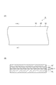
- (A) is a top view showing an embodiment of a temporary fixing resin film sheet having a first layer and a second layer, and (B) is along the II line in (A). It is a schematic cross section.
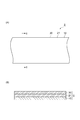
- (A) is a top view showing an embodiment of the first resin sheet, and (B) is a schematic cross-sectional view taken along line II-II in (A).
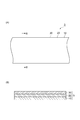
- (A) is a top view showing an embodiment of the second resin sheet, and (B) is a schematic cross-sectional view taken along line III-III of (A).
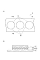
- (A) is a top view which shows other embodiment of the resin film sheet for temporary fixing which concerns on this invention,
- (B) is a schematic cross section along the IV-IV line of (A).
- FIG. It is a schematic cross section for explaining one embodiment of a separation process for separating the processed electronic component from the support and the temporarily fixing resin film. It is a schematic cross section for explaining one embodiment of a manufacturing method of an electronic device.
- the temporarily fixing resin film includes a first layer containing a first thermoplastic resin and a second layer containing a second thermoplastic resin and a curable component.
- FIG. 1A is a top view showing one embodiment of the temporarily fixing resin film of the present embodiment
- FIG. 1B is a schematic cross-sectional view taken along the line II of FIG. 1A. is there.
- the temporary fixing resin film sheet 1 shown in FIG. 1 includes a support film 10, a first layer 21, a second layer 22, and a support film 10 in this order, and includes a first layer 21 and a second layer 22.
- the temporary fixing resin film 20 is provided.
- the temporary fixing resin film according to the present embodiment has two layers having different compositions, so that the peel strength of the pressure-sensitive adhesive electronic component surface and the peel strength of the pressure-sensitive adhesive support surface can be adjusted. It can peel easily from both the electronic component currently fixed to the support body and the support body through the resin film. Further, since it is a film-like pressure-sensitive adhesive, it is easier to control the film thickness, and the variation in thickness between individual electronic components can be reduced. Further, the temporarily fixing resin film according to the present embodiment can be bonded onto an electronic component or a support by a simple method such as laminating, and is excellent in workability.
- the first layer includes a first thermoplastic resin (hereinafter also referred to as (a1) a thermoplastic resin).
- a1 a thermoplastic resin
- the thermoplastic resin can be used without particular limitation as long as it is a resin having thermoplasticity at least before the film is laminated on the electronic component or the support.
- the thermoplastic resin may be a resin that forms a crosslinked structure by heating or the like.
- thermoplastic resin a polymer having a crosslinkable functional group
- examples of the polymer having a crosslinkable functional group include thermoplastic polyimide resin, (meth) acrylic copolymer having a crosslinkable functional group, urethane resin polyphenylene ether resin, polyetherimide resin, phenoxy resin, and modified polyphenylene ether resin. It is done. Among these, a (meth) acrylic copolymer having a crosslinkable functional group is preferable. In the present specification, (meth) acryl is used to mean either acrylic or methacrylic.
- a thermoplastic resin may be used individually by 1 type, and may be used in combination of 2 or more type.
- the (meth) acrylic copolymer having a crosslinkable functional group one obtained by a polymerization method such as pearl polymerization or solution polymerization may be used, or a commercially available product may be used.
- the polymer having a crosslinkable functional group may have a crosslinkable functional group in the polymer chain or at the end of the polymer chain.
- the crosslinkable functional group include an epoxy group, an alcoholic hydroxyl group, a phenolic hydroxyl group, and a carboxyl group.
- a crosslinkable functional group may be used individually by 1 type, and may be used in combination of 2 or more type.
- the glass transition temperature of the thermoplastic resin (hereinafter sometimes referred to as “Tg”) is preferably ⁇ 50 ° C. to 50 ° C., more preferably ⁇ 30 ° C. to 20 ° C. . If Tg is in such a range, it is possible to obtain more sufficient fluidity while suppressing deterioration in handleability due to excessive increase in the tack force of the first layer, and further the elasticity of the sheet after curing. Since a rate can be made lower, it can further suppress that peeling strength becomes high too much.
- Tg is a midpoint glass transition temperature value when the thermoplastic resin is measured using differential scanning calorimetry (DSC, for example, “Thermo Plus 2” manufactured by Rigaku Corporation). Specifically, the Tg is a midpoint glass transition calculated by a method according to JIS K 7121: 1987 by measuring a change in calorie under conditions of a temperature increase rate of 10 ° C./min and a measurement temperature of ⁇ 80 to 80 ° C. Temperature.
- the weight average molecular weight of the thermoplastic resin is not particularly limited, and is preferably 100,000 to 1,200,000, more preferably 200,000 to 1,000,000. When the weight average molecular weight of the thermoplastic resin is in such a range, it becomes easier to ensure film formability and fluidity.
- the weight average molecular weight is a polystyrene conversion value using a standard polystyrene calibration curve by gel permeation chromatography (GPC).
- the first layer comprises (a1) a thermoplastic resin and, if necessary, a silicone compound (hereinafter sometimes referred to as (a2) silicone compound), a curing accelerator (hereinafter referred to as (a3) a curing accelerator). In some cases) and other ingredients.
- a silicone compound hereinafter sometimes referred to as (a2) silicone compound
- a curing accelerator hereinafter referred to as (a3) a curing accelerator
- the silicone compound can be used without particular limitation as long as it has a polysiloxane structure.
- silicone modified resin straight silicone oil, non-reactive modified silicone oil, reactive modified silicone oil and the like can be mentioned.
- a silicone compound can be used individually by 1 type or in combination of 2 or more types.
- the resin film for temporary fixing is easily removed from the semiconductor chip, the sealing body, and the support without using a solvent even at a low temperature of 100 ° C. or lower. It becomes possible to peel.
- the silicone compound used in the present embodiment is a silicone-modified resin
- silicone-modified resin there is no particular limitation as long as it is a resin modified with silicone.
- a silicone-modified alkyd resin is preferable.
- the first layer contains the silicone-modified alkyd resin, the temporary fixing resin film can be more easily peeled off without using a solvent when peeling the resin film for temporary fixing from the electronic component.
- a method for obtaining a silicone-modified alkyd resin for example, (i) a normal synthesis reaction for obtaining an alkyd resin, that is, when reacting a polyhydric alcohol with a fatty acid, a polybasic acid, etc., an organopolysiloxane is used as an alcohol component. The method of making it react simultaneously, (ii) The method of making organopolysiloxane react with the general alkyd resin synthesized beforehand.
- Examples of the polyhydric alcohol used as a raw material for the alkyd resin include dihydric alcohols such as ethylene glycol, diethylene glycol, triethylene glycol, propylene glycol, trimethylene glycol, tetramethylene glycol, and neopentyl glycol, glycerin, trimethylolethane, Examples thereof include trihydric alcohols such as trimethylolpropane, and tetrahydric or higher polyhydric alcohols such as diglycerin, triglycerin, pentaerythritol, dipentaerythritol, mannitol, and sorbit. These may be used individually by 1 type and may be used in combination of 2 or more type.
- polybasic acid used as a raw material for the alkyd resin examples include aromatic polybasic acids such as phthalic anhydride, terephthalic acid, isophthalic acid, and trimetic anhydride, and aliphatic saturated polybasic acids such as succinic acid, adipic acid, and sebacic acid.
- aromatic polybasic acids such as phthalic anhydride, terephthalic acid, isophthalic acid, and trimetic anhydride
- aliphatic saturated polybasic acids such as succinic acid, adipic acid, and sebacic acid.
- Aliphatic unsaturated polybasic acids such as basic acid, maleic acid, maleic anhydride, fumaric acid, itaconic acid, citraconic anhydride, cyclopentadiene-maleic anhydride adduct, terpene-maleic anhydride adduct, rosin-maleic anhydride
- polybasic acids by Diels-Alder reaction such as acid ad
- the alkyd resin may further contain a modifying agent or a crosslinking agent.
- Denaturing agents include octylic acid, lauric acid, palmitic acid, stearic acid, oleic acid, linoleic acid, linolenic acid, eleostearic acid, ricinoleic acid, dehydrated ricinoleic acid, coconut oil, linseed oil, gill oil, castor oil, dehydrated Castor oil, soybean oil, safflower oil, and these fatty acids can be used. These may be used individually by 1 type and may be used in combination of 2 or more type.
- crosslinking agent examples include amino resins such as melamine resins and urea resins, urethane resins, epoxy resins, and phenol resins. Among these, amino resins are preferred because amino alkyd resins crosslinked with amino resins are obtained.
- a crosslinking agent may be used individually by 1 type, and may be used in combination of 2 or more type.
- the silicone-modified alkyd resin can be used in combination with an acidic catalyst as a curing catalyst.
- an acidic catalyst there is no restriction
- an acidic catalyst for example, an organic acidic catalyst such as p-toluenesulfonic acid and methanesulfonic acid is suitable.
- An acidic catalyst may be used individually by 1 type, and may be used in combination of 2 or more type.
- silicone-modified alkyd resin examples include Tesfine TA31-209E (trade name, manufactured by Hitachi Chemical Co., Ltd.).
- silicone compound used in the present embodiment is a modified silicone oil
- polyether-modified silicone, alkyl-modified silicone, and epoxy-modified silicone are preferable.
- Any silicone can be used without particular limitation as long as it is compatible with the high molecular weight substance.
- silicone SH-3773M, L-7001, SH-550, SH-710 manufactured by Toray Dow Corning Co., Ltd., X-22-163, KF-105, X-22-163B manufactured by Shin-Etsu Silicone Co., Ltd., X-22-163C, BYK-UV3500 manufactured by BYK, and the like.
- the blending amount of the (a2) silicone compound in the first layer is preferably 0 to 100 parts by mass and more preferably 2 to 80 parts by mass with respect to 100 parts by mass of the (a1) thermoplastic resin. (A2) If the compounding amount of the silicone compound is within the above range, it is possible to achieve both higher adhesion between the adhesiveness during processing of the electronic component and the peelability after processing.
- curing accelerator examples include imidazoles, dicyandiamide derivatives, dicarboxylic acid dihydrazide, triphenylphosphine, tetraphenylphosphonium tetraphenylborate, 2-ethyl-4-methylimidazole-tetraphenylborate, 1,8-diazabicyclo. [5,4,0] undecene-7-tetraphenylborate and the like. These may be used individually by 1 type and may be used in combination of 2 or more type.
- thermoplastic resin contains a (meth) acrylic copolymer having an epoxy group
- a curing accelerator for accelerating the curing of the epoxy group contained in the acrylic copolymer is included. Is preferred.
- the blending amount of (a3) curing accelerator in the first layer is preferably 0.01 to 2.0 parts by mass with respect to 100 parts by mass of (a1) thermoplastic resin.
- A3 If the blending amount of the curing accelerator is 0.01 parts by mass or more with respect to 100 parts by mass of (a1) thermoplastic resin, the first layer is sufficiently cured in the thermal history in the manufacturing process of the semiconductor element. Therefore, the electronic component and the support can be more reliably fixed. If the blending amount of (a3) curing accelerator is 2.0 parts by mass or less with respect to 100 parts by mass of (a1) thermoplastic resin, the melt viscosity of the resin film for temporary fixing is unlikely to increase due to heating during the manufacturing process. Therefore, the storage stability of the film tends to be further improved.
- Other components include inorganic fillers, organic fillers, silane coupling agents, curable components, and the like.
- the inorganic filler examples include metal fillers such as silver powder, gold powder, and copper powder; non-metallic inorganic fillers such as silica, alumina, boron nitride, titania, glass, iron oxide, and ceramic.
- the inorganic filler can be selected according to the desired function.
- the metal filler can be added for the purpose of imparting thixotropy to the film.
- Nonmetallic inorganic fillers can be added for the purpose of imparting low thermal expansion and low hygroscopicity to the film.
- An inorganic filler may be used individually by 1 type, and may be used in combination of 2 or more type.
- the inorganic filler preferably has an organic group on the surface.
- an organic group By modifying the surface of the inorganic filler with an organic group, it is easy to improve the dispersibility in an organic solvent and the adhesion and heat resistance of the film when preparing a resin composition for forming a film. It becomes.
- the inorganic filler having an organic group on the surface can be obtained, for example, by mixing a silane coupling agent represented by the following general formula (B-1) and an inorganic filler and stirring at a temperature of 30 ° C. or higher. .
- the modification of the surface of the inorganic filler with an organic group can be confirmed by UV (ultraviolet) measurement, IR (infrared) measurement, XPS (X-ray photoelectron spectroscopy) measurement, or the like.
- X represents an organic group selected from the group consisting of a phenyl group, a glycidoxy group, an acryloyl group, a methacryloyl group, a mercapto group, an amino group, a vinyl group, an isocyanate group, and a methacryloxy group;
- R 11 , R 12 and R 13 each independently represents an alkyl group having 1 to 10 carbon atoms.
- alkyl group having 1 to 10 carbon atoms examples include methyl group, ethyl group, propyl group, butyl group, pentyl group, hexyl group, heptyl group, octyl group, nonyl group, decyl group, isopropyl group and isobutyl group. It is done.
- the alkyl group having 1 to 10 carbon atoms is preferably a methyl group, an ethyl group or a pentyl group from the viewpoint of easy availability.
- X is preferably an amino group, a glycidoxy group, a mercapto group, or an isocyanate group, and more preferably a glycidoxy group or a mercapto group.
- s is preferably 0 to 5, and more preferably 0 to 4, from the viewpoint of suppressing film fluidity at high heat and improving heat resistance.
- Preferred silane coupling agents are, for example, trimethoxyphenylsilane, dimethyldimethoxyphenylsilane, triethoxyphenylsilane, dimethoxymethylphenylsilane, vinyltrimethoxysilane, vinyltriethoxysilane, vinyltris (2-methoxyethoxy) silane, N- (2-aminoethyl) -3-aminopropylmethyldimethoxysilane, N- (2-aminoethyl) -3-aminopropyltrimethoxysilane, 3-aminopropyltriethoxysilane, 3-aminopropyltrimethoxysilane, 3- Glycidoxypropyltrimethoxysilane, 3-glycidoxypropylmethyldimethoxysilane, 2- (3,4-epoxycyclohexyl) ethyltrimethoxysilane, 3-isocyanatopropyltrieth
- 3-aminopropyltriethoxysilane, 3-glycidoxypropyltrimethoxysilane, 3-isocyanatopropyltriethoxysilane, and 3-mercaptopropyltrimethoxysilane are preferable, and trimethoxyphenylsilane, 3-glycidoxy More preferred are propyltrimethoxysilane and 3-mercaptopropyltrimethoxysilane.
- a silane coupling agent may be used individually by 1 type, and may be used in combination of 2 or more type.
- the amount of the coupling agent used is preferably 0.01 to 50 parts by weight, and 0.05 parts by weight with respect to 100 parts by weight of the inorganic filler, from the viewpoint of balancing the effect of improving heat resistance and storage stability. Part to 20 parts by weight is more preferable, and from the viewpoint of improving heat resistance, 0.5 to 10 parts by weight is still more preferable.
- the blending amount of the inorganic filler in the first layer is 300 with respect to 100 parts by mass of (a1) thermoplastic resin from the viewpoint of improving the handleability of the temporarily fixing resin film in the B-stage state and improving the low thermal expansion. It is preferably no greater than 200 parts by mass, more preferably no greater than 200 parts by mass, and even more preferably no greater than 100 parts by mass.
- the minimum of content of an inorganic filler does not have a restriction
- Examples of the organic filler include carbon, rubber filler, silicone fine particles, polyamide fine particles, and polyimide fine particles.
- the blending amount of the organic filler is preferably 300 parts by mass or less, more preferably 200 parts by mass or less, and still more preferably 100 parts by mass or less with respect to 100 parts by mass of the (a1) thermoplastic resin.
- the first layer can contain a curable component such as an epoxy resin, a phenol resin, or a bismaleimide resin.
- the thickness of the first layer 21 is not particularly limited. From the viewpoint of sufficiently embedding unevenness on the surface of an electronic component such as a semiconductor element, the thickness of the first layer 21 is the thickness after drying and the unevenness on the surface of the electronic component such as a semiconductor element. Is preferably equal to or less than 10 to 350 ⁇ m. If the thickness is 10 ⁇ m or more, there will be less variation in thickness at the time of coating, and since the thickness is sufficient, the strength of the film or the cured product of the film will be good, and electronic components such as semiconductor elements will Unevenness on the surface can be embedded more sufficiently.
- the thickness is 350 ⁇ m or less, it is difficult to be crushed when bonded to the second layer 22, so that the thickness of the temporarily fixing resin film is less likely to vary, and the amount of residual solvent in the film is reduced by sufficient drying. It becomes easy to reduce, and foaming when the cured product of the film is heated can be further reduced.
- the second layer includes a second thermoplastic resin (hereinafter also referred to as (b1) thermoplastic resin) and a curable component (hereinafter also referred to as (b2) curable component).
- a second thermoplastic resin hereinafter also referred to as (b1) thermoplastic resin
- a curable component hereinafter also referred to as (b2) curable component
- thermoplastic resin can be used without particular limitation as long as it is a resin having thermoplasticity at least before the film is laminated on the electronic component or the support.
- the thermoplastic resin may be a resin that forms a crosslinked structure by heating or the like.
- the polymer (b1) used in the present embodiment can be a polymer having a crosslinkable functional group.
- the polymer having a crosslinkable functional group include thermoplastic polyimide resin, (meth) acrylic copolymer having a crosslinkable functional group, urethane resin polyphenylene ether resin, polyetherimide resin, phenoxy resin, and modified polyphenylene ether resin. It is done. Among these, a (meth) acrylic copolymer having a crosslinkable functional group is preferable.
- the above resins may be used alone or in combination of two or more.
- the (meth) acrylic copolymer having a crosslinkable functional group one obtained by a polymerization method such as pearl polymerization or solution polymerization may be used, or a commercially available product may be used.
- the polymer having a crosslinkable functional group may have a crosslinkable functional group in the polymer chain or at the end of the polymer chain.
- the crosslinkable functional group include an epoxy group, an alcoholic hydroxyl group, a phenolic hydroxyl group, and a carboxyl group.
- a carboxyl group is preferable.
- the carboxyl group can be introduced into the polymer chain by using acrylic acid.
- the polymer having a crosslinkable functional group is preferably a (meth) acrylic copolymer having a carboxyl group, for example, a (meth) acrylic acid ester copolymer having a carboxyl group or a (meth) acrylic having a carboxyl group. Mention may be made of copolymers. Among these, a (meth) acrylic acid ester copolymer having a carboxyl group is preferable.
- said (meth) acrylic copolymer what has acrylic acid ester as a main component is mentioned, For example, the copolymer of butyl acrylate and / or ethyl acrylate, and acrylonitrile is mentioned.
- the Tg of the thermoplastic resin is preferably ⁇ 50 ° C. to 50 ° C., more preferably ⁇ 40 ° C. to 20 ° C. If Tg is in such a range, it is possible to obtain more sufficient fluidity while suppressing the tackiness of the second layer from being increased excessively and deteriorating the handleability. Since the elasticity modulus of a layer can be made lower, it can suppress more that peeling strength becomes high too much.
- the weight average molecular weight of the thermoplastic resin is not particularly limited, and is preferably 100,000 to 1,200,000, more preferably 300,000 to 1,000,000. When the weight average molecular weight of the thermoplastic resin is in such a range, it becomes easy to ensure film formability and fluidity.
- the curable component is not particularly limited, and a thermosetting resin is preferable.
- thermosetting resin examples include an epoxy resin, an acrylic resin, a silicone resin, a phenol resin, a thermosetting polyimide resin, a polyurethane resin, a melamine resin, and a urea resin. These may be used alone or in combination of two or more. Can also be used.
- the thermosetting resin is particularly preferably an epoxy resin from the viewpoint of obtaining a second layer excellent in heat resistance, workability and reliability.
- the epoxy resin is not particularly limited as long as it is cured and has a heat resistance.
- a bifunctional epoxy resin such as a bisphenol A type epoxy, a novolac type epoxy resin such as a phenol novolac type epoxy resin, a cresol novolak type epoxy resin, or the like can be used.
- a polyfunctional epoxy resin such as a polyfunctional epoxy resin, a glycidyl amine type epoxy resin, a heterocyclic ring-containing epoxy resin, an alicyclic epoxy resin, can be applied to the epoxy resin.
- Epicoat series (Epicoat 807, Epicoat 815, Epicoat 825, Epicoat 827, Epicoat 828, Epicoat 834, Epicoat 1001, Epicoat 1004, Epicoat 1007, Epicoat 1009, “Epicoat” manufactured by Japan Epoxy Resin Co., Ltd. Are registered trademarks), Dow Chemical Company, DER-330, DER-301, DER-361, and Nippon Steel & Sumikin Chemical Co., Ltd., YD8125, YDF8170, and the like.
- Examples of the phenol novolac type epoxy resin include Epicoat 152 and Epicoat 154 manufactured by Japan Epoxy Resin Co., Ltd., EPPN-201 manufactured by Nippon Kayaku Co., Ltd., and DEN-438 manufactured by Dow Chemical Co., Ltd.
- Examples of the o-cresol novolac type epoxy resin include EOCN-102S, EOCN-103S, EOCN-104S, EOCN-1012, EOCN-1025, EOCN-1027 manufactured by Nippon Kayaku Co., Ltd., YDCN701 manufactured by Nippon Steel & Sumikin Chemical Co., Ltd. YDCN702, YDCN703, YDCN704, etc. are mentioned.
- Epon 1031S manufactured by Japan Epoxy Resin Co., Ltd., Araldite 0163 manufactured by Ciba Specialty Chemicals Co., Ltd., Denacol EX-611, EX-614, EX-614B, EX-622 manufactured by Nagase ChemteX Corporation. , EX-512, EX-521, EX-421, EX-411, EX-321 and the like ("Araldite” and "Denacol" are registered trademarks).
- amine type epoxy resin Epicoat 604 manufactured by Japan Epoxy Resin Co., Ltd., YH-434 manufactured by Toto Kasei Co., Ltd., TETRAD-X and TETRAD-C manufactured by Mitsubishi Gas Chemical Co., Ltd., ELM- manufactured by Sumitomo Chemical Co., Ltd. 120 etc. are mentioned.
- heterocyclic ring-containing epoxy resin include Araldite PT810 manufactured by Ciba Specialty Chemicals, ERL4234, ERL4299, ERL4221, and ERL4206 manufactured by UCC. These epoxy resins may be used individually by 1 type, and may be used in combination of 2 or more type.
- thermosetting resin When using an epoxy resin as the thermosetting resin, it is preferable to use an epoxy resin curing agent together.
- the epoxy resin curing agent a known curing agent that is usually used can be used.
- the epoxy resin curing agent include bisphenols having two or more phenolic hydroxyl groups in one molecule such as amines, polyamides, acid anhydrides, polysulfides, boron trifluoride, bisphenol A, bisphenol F, and bisphenol S, Phenol resins such as phenol novolac resin, bisphenol A novolak resin, and cresol novolac resin are listed.
- the epoxy resin curing agent is preferably a phenol resin such as a phenol novolac resin, a bisphenol A novolac resin, or a cresol novolac resin.
- Phenolite LF2882 Phenolite LF2822
- Phenolite TD-2090 Phenolite TD-2149
- Phenolite VH-4150 Phenolite
- the blending amount of the (b2) curable component in the second layer is preferably 10 to 500 parts by mass, more preferably 50 to 300 parts by mass with respect to 100 parts by mass of (b1) thermoplastic resin. If the blending amount of the curable component is within the above range, the temporarily fixing resin film can have sufficient low-temperature sticking property, heat resistance, curability and peelability. When the blending amount is 10 parts by mass or more, the sticking property to the support and the heat resistance are improved, the retention property at the time of back grinding is also improved, and the wafer tends to be hard to break.
- the blending amount is 500 parts by mass or less, the viscosity before curing is not excessively low, and the composition can be cured in a relatively short time, and the retainability of the electronic component to the support and the peelability from the support are improved. It tends to be compatible.
- the second layer may be a silicone compound (hereinafter also referred to as (b3) silicone compound), a curing accelerator (hereinafter, (B4) may be referred to as a curing accelerator) and may contain other components.
- a silicone compound hereinafter also referred to as (b3) silicone compound
- a curing accelerator hereinafter, (B4) may be referred to as a curing accelerator
- silicone compound those mentioned above as the (a2) silicone compound can be used.
- the temporary fixing resin film can be easily removed from the semiconductor chip, the sealing body, and the support without using a solvent even at a low temperature of 100 ° C. or lower. It becomes possible to peel.
- the blending amount of the (b3) silicone compound in the second layer is preferably 0 to 100 parts by mass, more preferably 2 to 80 parts by mass with respect to 100 parts by mass of (b1) the thermoplastic resin. (B3) If the compounding amount of the silicone compound is within the above range, it is possible to achieve both adhesiveness during processing of electronic parts and peelability after processing.
- thermoplastic resin contains a (meth) acrylic copolymer having an epoxy group
- curing accelerator that accelerates the curing of the epoxy group contained in the acrylic copolymer. Is preferred.
- the blending amount of (b4) curing accelerator in the second layer is preferably 0.01 to 2.0 parts by mass with respect to 100 parts by mass of (b1) thermoplastic resin.
- (B4) When the blending amount of the curing accelerator is 0.01 parts by mass or more with respect to 100 parts by mass of (b1) thermoplastic resin, the second layer is sufficiently cured in the thermal history in the manufacturing process of the semiconductor element. Therefore, the electronic component and the support can be more reliably fixed. If the blending amount of (b4) curing accelerator is 2.0 parts by mass or less with respect to 100 parts by mass of (b1) thermoplastic resin, the melt viscosity of the resin film for temporary fixing is unlikely to increase due to heating during the manufacturing process. Therefore, the storage stability of the film tends to be further improved.
- Other components include inorganic fillers, organic fillers, silane coupling agents, and the like.
- the blending amount of the inorganic filler in the second layer is 300 parts by mass with respect to 100 parts by mass of (b1) thermoplastic resin from the viewpoint of improving the handleability of the temporarily fixing resin film in the B-stage state and improving the low thermal expansion. Part or less, preferably 200 parts by weight or less, more preferably 100 parts by weight or less. There is no restriction
- the blending amount of the organic filler is preferably 300 parts by mass or less, more preferably 200 parts by mass or less, and still more preferably 100 parts by mass or less with respect to (b1) 100 parts by mass of the thermoplastic resin.
- the blending amount of the organic filler is preferably 300 parts by mass or less, more preferably 200 parts by mass or less, and still more preferably 100 parts by mass or less with respect to (b1) 100 parts by mass of the thermoplastic resin.
- the thickness of the second layer 22 is not particularly limited, and is preferably 10 to 350 ⁇ m from the viewpoint of sufficiently fixing the electronic component and the support for transportation. If the thickness is 10 ⁇ m or more, there will be less variation in thickness at the time of coating, and since the thickness is sufficient, the strength of the film or the cured product of the film will be good, and support for electronic parts and transportation The body can be more sufficiently fixed. If the thickness is 350 ⁇ m or less, it is difficult to be crushed when bonded to the first layer 21, so that the thickness of the temporarily fixing resin film is less likely to vary, and the amount of residual solvent in the film is reduced by sufficient drying. It becomes easy to reduce, and foaming when the cured product of the film is heated can be further reduced.
- the thickness ratio between the first layer 21 and the second layer 22 preferably satisfies the relationship of the formula (1), and more preferably satisfies the relationship of the formula (2).
- a represents the thickness of the first layer 21, and b represents the thickness of the second layer 22.
- the ratio of the thicknesses of the first layer 21 and the second layer 22 is within the above range, the unevenness on the surface of the electronic component such as a semiconductor element can be sufficiently embedded in the temporarily fixing resin film. There is a tendency that the carrier and the carrier for transportation can be sufficiently fixed.
- the shear viscosity before curing of the first layer 21 is preferably 20000 Pa ⁇ s or less at 120 ° C., and more preferably 18000 Pa ⁇ s or less. If the shear viscosity at 120 ° C. is 20000 Pa ⁇ s or less, for example, it is sufficient when a pressure of 0.02 to 0.2 MPa is applied for 1 to 5 minutes under the conditions of 70 to 150 ° C. and 5 to 15 mbar. Therefore, the embedding property of the electronic component having bumps and other irregularities is further improved, and it is easier to press-bond to the electronic component without generating a gap.
- the shear viscosity at 120 ° C. may be 500 Pa ⁇ s or more.
- the second layer 22 preferably has a shear viscosity of 200 to 30000 Pa ⁇ s at 120 ° C., preferably 400 to 27000 Pa ⁇ s at 120 ° C., from the viewpoint of the handleability of the film or the adhesion to the support. It is more preferable.
- the shear viscosity is 200 Pa ⁇ s or more, the handleability of the film is further improved, and when the shear viscosity is 30000 Pa ⁇ s or less, sufficient adhesiveness is easily obtained.
- the above shear viscosity is measured when ARES (Rheometric Scientific Co., Ltd.) is used and the temperature is increased at a rate of temperature increase of 20 ° C./min while applying 5% strain to the temporarily fixing resin film. Mean value.
- the storage modulus of the first layer 21 after curing is preferably 0.1 to 1000 MPa at 25 ° C., more preferably 1 to 900 MPa. If the storage elastic modulus at 25 ° C. is 0.1 MPa or more, it is difficult for adhesive residue to occur in the electronic component during the peeling process, and if the elastic modulus at 25 ° C. is 1000 MPa or less, the electronic component having bumps and other irregularities during the peeling step Difficult to break bumps and other irregularities. That is, in the present embodiment, the first layer can be a layer attached to the electronic component.
- the storage modulus of the second layer 22 after curing is preferably 100 MPa or more at 25 ° C., more preferably 200 MPa or more. If the storage elastic modulus at 25 ° C. is 100 MPa or more, the electronic component and the support tend to be sufficiently fixed when the electronic component is thinned.
- the storage elastic modulus after curing may be 6000 MPa or less at 25 ° C.
- the relationship between the storage elastic modulus after curing of the first layer 21 and the storage elastic modulus after curing of the second layer 22 is higher than the storage elastic modulus after curing of the first layer 21. It is preferred that the storage modulus of the layer 22 after curing is greater. If the storage elastic modulus after curing is such a relationship, it is possible to further reduce the possibility of adhesive residue remaining on the electronic component during the peeling process, and further prevent breakage of bumps and the like on the electronic component. In addition, when the electronic component is thinned, the electronic component and the support can be more firmly fixed.
- the storage elastic modulus means a measured value when measured using a dynamic viscoelasticity measuring apparatus (manufactured by UBM Co., Ltd.) while increasing the temperature at a rate of temperature increase of 3 ° C./min.
- the first layer 21 preferably has a 30 ° peel strength with respect to an electronic component such as a silicon wafer of 500 N / m or less at 25 ° C., more preferably 450 N / m or less. If the 30 ° peel strength is 500 N / m or less, the first layer and the electronic component can be further peeled without any adhesive residue, and the possibility that the electronic component breaks during peeling tends to be reduced.
- the 30 ° peel strength may be 10 N / m or more.
- 30 ° peel strength can be measured as follows. Grooves having a width of 40 ⁇ m and a depth of 40 ⁇ m are formed at intervals of 100 ⁇ m on the surface of a 625 ⁇ m thick silicon mirror wafer (6 inches) by blade dicing.
- the stepped silicon mirror wafer thus produced is placed on the stage of a vacuum laminator (manufactured by NPC Corporation, LM-50X50-S) so that the level difference of the stepped silicon mirror wafer becomes the upper surface.
- the fixing resin film is installed so that the first layer is attached to the stepped silicon mirror wafer side. This was heated and pressurized for 2 minutes at a temperature of 120 ° C.
- the obtained measurement sample is cured and cut into a width of 10 mm. This is subjected to a peel test at a speed of 300 mm / min with a peel tester set so that the peel angle is 30 °, and the peel strength at that time is set to 30 ° peel strength.
- the second layer 22 preferably has a 90 ° peel strength at 25 ° C. of 5 N / m to 200 N / m, more preferably 6 to 180 N / m, on a support, for example, a silicon mirror wafer. If the 90 ° peel strength is within the above range, the second layer and the support can be peeled without any adhesive residue. If the 90 ° peel strength is 5 N / m or more, the electronic component and the support can be more firmly fixed in the grinding process, and if it is 200 N / m or less, the temporarily fixing resin film is peeled off. In this case, the adhesive layer can be peeled off without any adhesive residue between the second layer and the support, and the possibility that the film remains on the support can be further reduced.
- 90 ° peel strength can be measured as follows.
- a 625 ⁇ m-thick silicon mirror wafer (6 inches) is placed on the stage of a vacuum laminator (manufactured by NPC, LM-50X50-S), and the temporarily fixing resin film according to this embodiment is placed on the second Install so that the layer sticks to the silicon mirror wafer side.
- the obtained measurement sample is cured and cut into a width of 10 mm.
- This is subjected to a peel test at a speed of 300 mm / min with a peel tester set so that the peel angle is 90 °, and the peel strength at that time is set to 90 ° peel strength.
- the temporarily fixing resin film sheet 1 according to this embodiment can be manufactured, for example, from a first resin sheet 2 shown in FIG. 2 and a second resin sheet 3 shown in FIG.
- FIG. 2 (A) is a top view showing an embodiment of the first resin sheet
- FIG. 2 (B) is a schematic sectional view taken along the line II-II in FIG. 2 (A).
- the first resin sheet 2 shown in FIG. 2 includes a support film 10 having releasability, a first layer 21 provided on the support film 10, and the side opposite to the support film 10 of the first layer 21. And a protective film 30 provided on the surface.
- FIG. 3A is a top view showing an embodiment of the second resin sheet
- FIG. 3B is a schematic cross-sectional view taken along line III-III in FIG. 3A.
- the second resin sheet 3 shown in FIG. 3 includes a support film 10 having releasability, a second layer 22 provided on the support film 10, and the side opposite to the support film 10 of the second layer 22. And a protective film 30 provided on the surface.
- the temporary fixing resin film sheet 1 peels the protective film 30 from the first resin sheet 2 and the second resin sheet 3, and the first layer 21 surface and the second layer 22 surface are separated by 60 ⁇ It can manufacture by bonding together by roll lamination etc. at 120 degreeC.
- Each of the first layer 21 and the second layer 22 according to the present embodiment is prepared by mixing and kneading the above-described components in an organic solvent to prepare a varnish, applying the produced varnish on the support film 10 and drying it. It can form by the method to do. Thus, the resin sheets 2 and 3 provided with the first layer 21 or the second layer 22 on the support film 10 are respectively produced.
- the organic solvent is not particularly limited, and can be determined in consideration of the volatility during film formation from the boiling point. Specifically, from the viewpoint of making the film hard to progress during film formation, methanol, ethanol, 2-methoxyethanol, 2-ethoxyethanol, 2-butoxyethanol, methyl ethyl ketone, acetone, methyl isobutyl ketone, toluene, xylene, etc.
- a relatively low boiling point solvent is preferred.
- a solvent having a relatively high boiling point such as dimethylacetamide, dimethylformamide, N-methylpyrrolidone and cyclohexanone. These solvent may be used individually by 1 type, and may be used in combination of 2 or more type.
- the solid concentration in the varnish is preferably 10 to 80% by mass.
- the above mixing and kneading can be performed by using a normal stirrer, a raking machine, a three-roller, a ball mill, or other dispersing machine, and appropriately combining them.
- the heat drying is not particularly limited as long as the solvent used is sufficiently volatilized, and can be performed usually by heating at 60 to 200 ° C. for 0.1 to 90 minutes.
- Protective film 30 can be attached to first layer 21 or second layer 22 provided on support film 10 as necessary.
- first resin sheet 2 or the second resin sheet 3 having the three-layer structure including the support film 10, the first layer 21 or the second layer 22, and the protective film 30 described above is obtained. be able to.
- the first resin sheet 2 or the second resin sheet 3 obtained in this way can be easily stored, for example, by winding it into a roll. Moreover, a roll-shaped film can be cut out into a suitable size and stored in a sheet shape. Moreover, the resin film sheet 1 for temporary fixing of this embodiment obtained by bonding these films can also be easily preserve
- the support film 10 is not particularly limited, and examples thereof include polyethylene terephthalate, polybutylene terephthalate, polyethylene naphthalate, polyethylene, polypropylene, polyamide, and polyimide.
- the support film 10 is preferably polyethylene terephthalate, polybutylene terephthalate, polyethylene naphthalate, polypropylene, polyamide, or polyimide from the viewpoint of excellent flexibility and toughness. Further, from the viewpoint of improving the peelability from the resin film (resin layer), it is preferable to use as the support film a film that has been subjected to a release treatment with a silicone compound, a fluorine compound, or the like.
- the thickness of the support film 10 may be appropriately changed depending on the intended flexibility, but is preferably 3 to 350 ⁇ m. If the thickness is 3 ⁇ m or more, the film strength is sufficient, and if it is 350 ⁇ m or less, sufficient flexibility tends to be obtained. From such a viewpoint, the thickness of the support film 10 is more preferably 5 to 200 ⁇ m, and further preferably 7 to 150 ⁇ m.
- the protective film 30 is not particularly limited, and examples thereof include polyethylene terephthalate, polybutylene terephthalate, polyethylene naphthalate, polyethylene, and polypropylene.
- the protective film 30 is preferably polyethylene terephthalate, polyethylene or polypropylene from the viewpoints of flexibility and toughness. Further, from the viewpoint of improving the peelability from the temporarily fixing resin film (resin layer), it is preferable to use as the protective film 30 a film that has been subjected to a release treatment with a silicone compound, a fluorine compound, or the like.
- the thickness of the protective film 30 can be appropriately set depending on the intended flexibility, and is preferably 10 to 350 ⁇ m, for example. If the thickness is 10 ⁇ m or more, the film strength becomes better, and if it is 350 ⁇ m or less, further flexibility is obtained. From such a viewpoint, the thickness of the protective film 30 is more preferably 15 to 200 ⁇ m, and further preferably 20 to 150 ⁇ m.
- FIG. 4 Another embodiment of the temporarily fixing resin film sheet is shown in FIG.
- the temporary fixing resin film sheet 4 shown in FIG. 4 is temporary except that the temporary fixing resin film 20 and the support film 10 on the second layer 22 side are preliminarily cut according to the shape of the member to be temporarily fixed. It has the same configuration as the fixing resin film sheet 1.
- FIG. 4 the outer edges of the temporarily fixed resin film 20 and the support film 10 that have been cut are removed, but the temporary fixing resin film and the support film are notched according to the shape of the temporarily fixed member. And the outer edge may be left.
- a resin film set including a first resin sheet 2 and a second resin sheet 3 can be mentioned.
- the first layer and the second layer of these resin sheets are bonded together and used as a temporary fixing resin film during use (when processing electronic components). it can.
- the electronic parts can be processed well at high temperatures, and can be easily peeled off from the processed electronic parts and the support even at room temperature. Thus, adhesive residue on the electronic component and the support can be prevented.
- the processing method of the electronic component using the temporarily fixing resin film according to this embodiment is roughly divided into the following four steps.
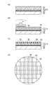
- FIG. 5 (A), 5 (B), and 5 (C) are schematic cross-sectional views for explaining an embodiment of a method for processing an electronic component, and FIG. 5 (D) shows an electron after processing. It is a top view which shows components.
- FIG. 5A a film-like temporary fixing material 40 having a two-layer configuration of a first layer 41 and a second layer 42 is interposed between the support 50 and the electronic component 60, and the support 50 The process of temporarily fixing the electronic component 60 is shown in FIG. At this time, the film-like temporary fixing material 40 is disposed so that the first layer 41 contacts the electronic component 60 side and the second layer 42 contacts the support 50 side.
- the thickness of the electronic component 60 is not particularly limited, but can be 600 to 800 ⁇ m.
- A-1) Formation of Temporary Fixing Material 40 on Support 50 By laminating the second layer 22 side of the temporarily fixing resin film 20 on the support 50 using a roll laminator, a vacuum laminator, or the like. A film-like temporary fixing material 40 can be provided.
- the material of the support in this embodiment is not particularly limited, and a substrate such as a silicon wafer, a glass wafer, or a quartz wafer can be used.
- the support may be subjected to a peeling treatment, and the peeling layer 52 is formed by peeling all or part of the surface of the support 50 as shown in FIG.
- the release agent used for the release treatment is not particularly limited.
- a surface modifier having a fluorine element, a polyolefin wax and silicone oil, a silicone oil containing a reactive group, and a silicone-modified alkyd resin have excellent release properties. Therefore, it is preferable.
- the pressure is 1 hPa or less, the pressure is 1 MPa, the pressure is 60 ° C. to 200 ° C., the holding time is 100 seconds to 300 seconds.
- the component 60 and the support body 50 are temporarily fixed via a film-like temporary fixing material 40.
- a vacuum laminator for example, a vacuum laminator LM-50 ⁇ 50-S (trade name) manufactured by NPC Corporation, or a vacuum laminator V130 (trade name) manufactured by Nichigo Morton Co., Ltd. can be used.
- the pressing conditions are an atmospheric pressure of 1 hPa or less, a pressure bonding temperature of 40 ° C. to 180 ° C., preferably 60 ° C. to 150 ° C., a laminating pressure of 0.01 to 0.5 MPa, preferably 0.1 to 0.5 MPa, and a holding time of 1 second to 600.
- the electronic component 60 and the support 50 are temporarily fixed via the film-like temporary fixing material 40 in seconds, preferably 30 to 300 seconds.
- Electronic components include semiconductor elements.
- the material of the electronic component is not particularly limited, and a substrate such as a silicon wafer, a glass wafer, a quartz wafer, or a semiconductor wafer can be used.
- the curing method is not particularly limited as long as the film is cured, and there is a method by heat or radiation irradiation.
- curing method curing by heat is preferable.
- the curing conditions are preferably 100 to 200 ° C. for 10 to 300 minutes, more preferably 20 to 210 minutes.
- the temperature is 100 ° C. or higher, the film is sufficiently cured and hardly causes a problem in the processing step.
- the temperature is 200 ° C.
- the temporary fixing material 40 is cured to become the temporary fixing material 70 including the cured first layer 71 and the cured second layer 72.
- the processing steps include grinding, electrode formation, metal wiring formation, protective film formation and the like used at the wafer level.
- a well-known grinding system can be utilized.
- the grinding is preferably performed while cooling the electronic component and a grindstone (such as diamond) with water.
- the back surface of the electronic component 80 that is, the surface of the electronic component 80 opposite to the side in contact with the film-like temporary fixing material 70 is ground by a grinder 90, for example, about 700 ⁇ m.
- the thickness is reduced to 100 ⁇ m or less.
- DGP-8761 (trade name) manufactured by DISCO Corporation can be cited, and the cutting conditions in this case can be arbitrarily selected according to the thickness of the desired electronic component and the grinding state.
- other processes include metal sputtering for forming electrodes, etc., wet etching for etching metal sputtering layers, application of resist for masking the formation of metal wiring, pattern formation by exposure / development, resist coating
- Known processes such as peeling, dry etching, formation of metal plating, silicon etching for TSV formation, and formation of an oxide film on the silicon surface can be mentioned.
- dry ion etching or a Bosch process or the like is performed on the back side of the thinned electronic component 80 to form a through hole, and then a process such as copper plating is performed to form a through electrode 82.
- a process such as copper plating is performed to form a through electrode 82.
- An example is shown.
- FIG. 5D is a top view of the electronic component 80 after processing.
- the processed electronic component 80 is further separated into semiconductor elements by dicing along a dicing line 84.
- FIG. 6 is a schematic cross-sectional view for explaining an embodiment of a separation step for separating the processed electronic component from the support and the film-like temporary fixing material.
- the separation process according to this embodiment includes a first peeling process for peeling the electronic component from the support and a second peeling process for peeling the film-like temporary fixing material from the support.
- the first peeling step is a step of peeling the electronic component processed in the processing step from the support, that is, a step of peeling the thinned electronic component from the support before dicing after various processing. It is.
- one of the electronic component or the support is fixed horizontally, the other is lifted with a certain angle from the horizontal direction, and a protective film is attached to the ground surface of the electronic component
- Examples of the method include a method of peeling the protective film from the support by a peel method, and the method can be employed without any particular limitation.
- peeling methods can be applied to this embodiment.
- a peeling method as shown in FIG. 6A, there is a method in which one of the electronic component 80 or the support 50 is fixed horizontally and the other is lifted at a certain angle from the horizontal direction. Thus, the electronic component 80 can be obtained (see FIG. 6C).
- a film-like temporary fixing material is formed using the temporary fixing resin film according to the present embodiment, so that processed electronic components in which residues such as adhesive residue are sufficiently reduced can be easily obtained. Obtainable.
- These peeling methods are usually carried out at room temperature, but may be carried out at a temperature that does not damage the electronic components of about 40 to 100 ° C.
- a debonder manufactured by SUSS Co., Ltd., DB12T
- a De-Bonding device manufactured by EVG, EVG805EZD
- EVG EVG805EZD
- the electronic component 80 is fixed horizontally, and the end of the film-like temporary fixing material 70 is set at a certain angle from the horizontal direction. By lifting, the electronic component 80 from which the temporarily fixing material is peeled can be obtained, and the support can be recovered.
- ⁇ (D) Cleaning step> A part of the temporarily fixed material tends to remain on the circuit forming surface of the electronic component.
- a cleaning process for removing the temporary fixing material can be provided.
- the temporary fixing material can be removed, for example, by washing the electronic component.
- the cleaning solution is not particularly limited as long as it is a cleaning solution that can remove a partially remaining temporarily fixing resin film.
- a cleaning liquid examples include the organic solvents that can be used for dilution of the resin film composition for temporary fixing. These organic solvents may be used individually by 1 type, and may be used in combination of 2 or more type.
- bases and acids may be added to the organic solvent.
- bases that can be used include amines such as ethanolamine, diethanolamine, triethanolamine, triethylamine, and ammonia; and ammonium salts such as tetramethylammonium hydroxide.
- acids organic acids such as acetic acid, oxalic acid, benzenesulfonic acid, and dodecylbenzenesulfonic acid can be used.
- the addition amount is preferably 0.01 to 10% by mass in the concentration in the cleaning solution.
- an existing surfactant may be added to the cleaning liquid in order to improve the removability of the residue.
- the cleaning method is not particularly limited, and examples thereof include a method of cleaning with a paddle using the above-described cleaning liquid, a cleaning method by spraying, and a method of immersing in a cleaning liquid tank.
- the temperature is preferably 10 to 80 ° C., preferably 15 to 65 ° C.
- washing with water or alcohol is performed, followed by drying to obtain a thin electronic component 80.
- residues such as adhesive residue can be sufficiently reduced, so that the cleaning step can be omitted.
- the processed electronic component 80 has through electrodes 82 formed in the same manner as described above, and is further separated into semiconductor elements by dicing along a dicing line 84 (see FIG. 6D).
- an electronic device can be manufactured by connecting the obtained semiconductor element to another semiconductor element or a semiconductor element mounting substrate.
- FIG. 7 is a schematic cross-sectional view for explaining an embodiment of a method for manufacturing an electronic device.
- a semiconductor element 100 in which the through electrode 86 is formed and separated into pieces by the above-described method is prepared (FIG. 7A).
- the electronic device device 120 can be obtained (FIG. 7B).
- polyimide resin PI-1 was a thermoplastic resin, and had a weight average molecular weight of 50,000 and Tg of 70 ° C. Polyimide resin PI-1 was prepared and used so that the solid content concentration in NMP was 50% by mass. In addition, the compounding quantity of PI-1 shown in Table 1 and 2 is a mass part of solid content.
- DBTA decamethylene bistrimellitic dianhydride
- Examples 1 to 11, Comparative Examples 1 and 2 [Preparation of resin film for temporary fixation]
- Varnishes for forming the first layer and the second layer were prepared with the composition of parts by mass shown in Tables 1 to 3.
- the prepared varnish was applied onto a release-treated surface of a release-treated polyethylene terephthalate film (Teijin DuPont Films, A31, thickness 38 ⁇ m), and dried by heating at 90 ° C. for 5 minutes and 140 ° C. for 5 minutes. .
- the said film was further bonded as a protective film on the resin layer, and the 1st resin sheet and the 2nd resin sheet with which the protective film and the support film were attached were obtained, respectively.
- the protective film was peeled off from each resin sheet, and the first layer and the second layer were bonded together by roll lamination at 60 ° C. to obtain each temporary fixing resin film.
- Thermoplastic resin HTR-280-CHN Acrylic rubber (manufactured by Nagase ChemteX Corporation) with a weight average molecular weight of 900,000 and Tg-28 ° C. by GPC HTR-280-Mw1: Acrylic rubber (manufactured by Nagase ChemteX Corporation) having a weight average molecular weight of 600,000 by GPC and Tg-28 ° C.
- HTR-860P-3CSP Acrylic rubber (manufactured by Nagase ChemteX Corporation) with GPC weight average molecular weight of 800,000 and Tg of 12 ° C HTR-860P-3CSP-30B: Acrylic rubber (manufactured by Nagase ChemteX Corporation) having a weight average molecular weight of 300,000 by GPC and Tg of 12 ° C
- Acrylic rubber K-1 Acrylic rubber synthesized above (weight average molecular weight by GPC of 300,000, Tg-20 ° C.)
- Acrylic rubber K-2 Acrylic rubber synthesized above (GPC weight average molecular weight 400,000, Tg-28 ° C.)
- Polyimide resin PI-1 Polyimide resin synthesized above (weight average molecular weight 50000 by GPC, Tg 70 ° C.)
- Curing component YDCN-700-10 Cresol novolac type polyfunctional epoxy resin (manufactured by Nippon Steel & Sumikin Chemical Co., Ltd.
- the shear viscosity before curing was evaluated by the following method.
- a single layer film for measurement in which either the first layer or the second layer is adjusted to a thickness of 120 ⁇ m is laminated at 80 ° C., and a rotary viscoelasticity measuring apparatus (ARES, manufactured by TA Instruments Inc., ARES). ) was used to measure the shear viscosity.
- ARES rotary viscoelasticity measuring apparatus
- the measurement method is “parallel plate”, the measurement jig is a circular jig with a diameter of 8 mm, the measurement mode is “Dynamic temperature ramp”, the frequency is 1 Hz, and the measurement single layer film is subjected to 5% distortion at 35 ° C.
- the temperature was raised to 120 ° C. at a rate of temperature increase of 20 ° C./min, and the viscosity of the film for measurement when it reached 120 ° C. was measured.
- Step embedding The step embedding property of the temporarily fixing resin film was evaluated by the following method.
- the second layer side of the temporarily fixing resin film was bonded to the surface of a 625 ⁇ m thick silicon mirror wafer (6 inches) by roll lamination at 80 ° C. to obtain a wafer with a temporarily fixing resin film.
- grooves having a width of 40 ⁇ m and a depth of 40 ⁇ m were formed at intervals of 100 ⁇ m on the surface of a 625 ⁇ m thick silicon mirror wafer (6 inches) by blade dicing.
- the first layer of the resin film for temporary fixing was installed so as to stick to the stepped silicon mirror wafer side. This was heat-pressed for 2 minutes at a temperature of 120 ° C. and a pressure of 0.1 MPa under the condition of 15 mbar, and vacuum laminated. Then, the state of the resin film for temporary fixing was confirmed using the ultrasonic microscope (SAM, Insight-300 by Insight Co., Ltd.).
- the evaluation criteria for embedding are as follows. A: The void ratio is less than 5%. B: Void ratio is 5% or more.
- the heat resistance at 200 ° C. of the temporarily fixing resin film was evaluated by the following method.
- a 625 ⁇ m thick silicon mirror wafer (6 inches) was cut into 25 mm square pieces by blade dicing. It roll-laminated at 80 degreeC so that the 2nd layer side of the resin film for temporary fixing might stick on the silicon mirror wafer surface cut into pieces.
- a glass slide having a thickness of 0.1 to 0.2 mm and a size of about 18 mm square is roll-laminated at 80 ° C. on the first layer side of the temporarily fixing resin film.
- a laminate sample sandwiched between a silicon wafer and a slide glass was produced. The obtained sample was heated at 130 ° C.
- the sample thus obtained was observed from the slide glass surface, the image was analyzed with a soft wafer such as Photoshop (registered trademark), and the heat resistance at 200 ° C. was determined from the proportion of voids in the total area of the temporary fixing resin film. Sex was evaluated.
- the evaluation criteria are as follows. A: The void ratio is less than 5%. B: Void ratio is 5% or more.
- the cut single-layer film for measurement was set in a dynamic viscoelastic device (product name: Rheogel-E4000, manufactured by UMB Co., Ltd.), applied with a tensile load, and measured at a frequency of 10 Hz and a heating rate of 3 ° C./min.
- the storage elastic modulus at 25 ° C. was measured.
- the 30 ° peel strength between the silicon wafer and the temporarily fixing resin film (first layer) was evaluated by the following method. Grooves having a width of 40 ⁇ m and a depth of 40 ⁇ m were formed at intervals of 100 ⁇ m on the surface of a 625 ⁇ m thick silicon mirror wafer (6 inches) by blade dicing. Place the stepped silicon mirror wafer thus prepared on the stage of a vacuum laminator (LM-50X50-S, manufactured by NPC, Inc.) so that the level difference is on the upper surface, and temporarily fix the resin film for fixing. The first layer was placed so as to stick to the stepped silicon mirror wafer side, heated and pressurized at 120 ° C.
- LM-50X50-S manufactured by NPC, Inc.
- the obtained sample was heated at 130 ° C. for 30 minutes and subsequently heated at 170 ° C. for 1 hour to be cured. This was further heated at 200 ° C. for 30 minutes, and then cut into a width of 10 mm to obtain a measurement film.
- the film for measurement was subjected to a peel test at a speed of 300 mm / min with a peel tester set so that the peel angle was 30 °, and the peel strength at that time was defined as 30 ° peel strength.
- the 90 ° peel strength between the silicon mirror wafer and the temporarily fixing resin film (second layer) was evaluated by the following method.
- a 625 ⁇ m thick silicon mirror wafer (6 inches) is placed on the stage of a vacuum laminator (manufactured by NPC, LM-50X50-S), and the second layer of the temporary fixing resin film is a silicon mirror wafer It was installed so as to stick to the side, heated and pressurized for 2 minutes at a temperature of 120 ° C. and a pressure of 0.1 MPa under the condition of 15 mbar, and vacuum laminated.
- the obtained sample was heated at 130 ° C. for 30 minutes and subsequently heated at 170 ° C. for 1 hour to be cured. This was further heated at 200 ° C.
- the film for measurement was subjected to a peel test at a speed of 300 mm / min with a peel tester set so that the peel angle was 90 °, and the peel strength at that time was defined as 90 ° peel strength.
- the silicon wafer was bonded to the step side so that the first layer of the temporarily fixing resin film of the support with the temporarily fixing resin film was in contact with a vacuum bonding apparatus (VE07-14 manufactured by Ayumi Industry Co., Ltd.). Under the condition of 5 mbar, the laminate was obtained by heating and pressing at a temperature of 120 ° C. and a pressure of 0.1 MPa for 2 minutes. The laminate thus obtained was heated at 130 ° C. for 30 minutes, and then heated at 170 ° C. for 1 hour to cure the temporarily fixing resin film. Then, after heating this at 200 ° C.
- a vacuum bonding apparatus VE07-14 manufactured by Ayumi Industry Co., Ltd.
- tweezers with a sharp tip are inserted between the step side of the silicon wafer and the first layer side of the temporarily fixing resin film, and the tweezers are moved along the outer edge. It was.
- the silicon wafer and the support that could be peeled without cracking were designated as A, and those that could not be peeled off or those that were damaged were designated as B.
- the temporary fixing resin films of the examples were excellent in the step embedding property and heat resistance of the silicon wafer. Also, the 30 ° peel strength between the silicon wafer and the first layer side of the temporarily fixing resin film is low, and the 90 ° peel strength between the silicon mirror wafer and the second layer side of the temporarily fixing resin film. Therefore, it was confirmed that the peelability was good.
Landscapes
- Chemical & Material Sciences (AREA)
- Organic Chemistry (AREA)
- Chemical Kinetics & Catalysis (AREA)
- Adhesives Or Adhesive Processes (AREA)
- Laminated Bodies (AREA)
- Adhesive Tapes (AREA)
- Mechanical Treatment Of Semiconductor (AREA)
- Container, Conveyance, Adherence, Positioning, Of Wafer (AREA)
Abstract
Description
(1/10)a≦b≦10a ・・・(1)
[式(1)中、aは第一の層の厚さを表し、bは第二の層の厚さを表す。]
厚さの比率が上記範囲内であれば、電子部品面の剥離強度と粘着剤の支持体面の剥離強度とを調整することが容易にできる。
本実施形態に係る仮固定用樹脂フィルムは、第一の熱可塑性樹脂を含む第一の層と、第二の熱可塑性樹脂及び硬化性成分を含む第二の層と、を備える。
第一の層は、第一の熱可塑性樹脂(以下、(a1)熱可塑性樹脂という場合もある。)を含む。(a1)熱可塑性樹脂としては、少なくともフィルムが電子部品又は支持体にラミネートされる前において熱可塑性を有している樹脂であれば特に制限なく用いることができる。熱可塑性樹脂は、加熱等により架橋構造を形成する樹脂であってもよい。

第二の層は、第二の熱可塑性樹脂(以下、(b1)熱可塑性樹脂という場合もある。)及び硬化性成分(以下、(b2)硬化性成分という場合もある。)を含む。
上記(メタ)アクリル共重合体としては、アクリル酸エステルを主成分とするものが挙げられ、例えば、ブチルアクリレート及び/又はエチルアクリレートとアクリロニトリルとの共重合体が挙げられる。
(1/10)a≦b≦10a・・・(1)
(1/5)a≦b≦6a・・・(2)
式中、aは第一の層21の厚さを示し、bは第二の層22の厚さを示す。
本実施形態に係る仮固定用樹脂フィルムシート1は、例えば、図2に示す第一の樹脂シート2と図3に示す第二の樹脂シート3とから製造することができる。
本実施形態に係る仮固定用樹脂フィルムを用いた電子部品の加工方法は、大きく分けて以下の4工程を備える。(a)電子部品と支持体とを仮固定用樹脂フィルムを介して仮固定する工程と、(b)支持体に仮固定された電子部品を加工する加工工程と、(c)加工された電子部品を支持体及び仮固定用樹脂フィルムから分離する分離工程と、(d)電子部品に残渣がある場合に洗浄する洗浄工程とを備える。
図5の(A)は、支持体50及び電子部品60の間に、第一の層41及び第二の層42の2層構成を有するフィルム状の仮固定材40を介在させ、支持体50に電子部品60を仮固定する工程を示す。この際、電子部品60側に第一の層41が、支持体50側に第二の層42が接触するように、フィルム状の仮固定材40を配置する。
ロールラミネーター、真空ラミネーターなどを用いて、支持体50上に仮固定用樹脂フィルム20の第二の層22側をラミネートすることによりフィルム状の仮固定材40を設けることができる。
次に、ウェハ接合装置又は真空ラミネーター上に、フィルム状の仮固定材40を形成した支持体50をセットし、第一の層41側に電子部品60をプレスで押圧して貼り付ける。
電子部品60と支持体50とをフィルム状の仮固定材40を介して仮固定した後、フィルム状の仮固定材40の硬化を行う。硬化方法はフィルムが硬化されれば特に制限されなく、熱又は放射線照射による方法がある。硬化方法としては、中でも、熱による硬化が好ましい。熱による硬化をする場合、硬化条件は、100~200℃で10~300分の硬化が好ましく、20~210分の硬化がより好ましい。温度が100℃以上であればフィルムが充分に硬化して加工工程で問題が起きにくく、200℃以下であればフィルムの硬化中にアウトガスが発生しにくく、フィルムの剥離を更に抑制できる。また、硬化時間が10分以上であれば加工工程で問題が起きにくく、300分以下であれば作業効率が悪化しにくい。仮固定材40は硬化することで、硬化した第一の層71と硬化した第二の層72を備える仮固定材70になる。
加工工程には、ウェハレベルで用いられる研削、電極形成、金属配線形成、保護膜形成等が含まれる。研削方式には特に制限はなく、公知の研削方式が利用できる。研削は電子部品と砥石(ダイヤモンド等)とに水をかけて冷却しながら行うことが好ましい。
図6は、加工された電子部品を支持体及びフィルム状の仮固定材から分離する分離工程の一実施形態を説明するための模式断面図である。本実施形態に係る分離工程は、支持体から電子部品を剥離する第一の剥離工程と、支持体からフィルム状の仮固定材を剥離する第二の剥離工程と、を含む。第一の剥離工程は、加工工程で加工を施した電子部品を支持体から剥離する工程、即ち、薄型化した電子部品に様々な加工を施した後、ダイシングする前に支持体から剥離する工程である。剥離方法としては、電子部品又は支持体の一方を水平に固定しておき、他方を水平方向から一定の角度を付けて持ち上げる方法、及び、電子部品の研削面に保護フィルムを貼り、電子部品と保護フィルムとをピール方式で支持体から剥離する方法等が挙げられ、特に制限なく採用することができる。
電子部品の回路形成面は仮固定材の一部が残存しやすい。剥離した電子部品の回路形成面に仮固定材が一部残存した場合、これを除去するための洗浄工程を設けることができる。仮固定材の除去は、例えば、電子部品を洗浄することにより行うことができる。
撹拌機、温度計、窒素置換装置(窒素流入管)、及び水分受容器付きの還流冷却器を備えたフラスコ内に、ジアミンであるBAPP(商品名、東京化成製、2,2-ビス[4-(4-アミノフェノキシ)フェニル]プロパン、分子量:410.51)10.26g(0.025mol)及び1,4-ブタンジオールビス(3-アミノプロピル)エーテル(東京化成製、商品名:B-12、分子量:204.31)5.10g(0.025mol)と、溶媒であるN-メチル-2-ピロリドン(NMP)100gとを仕込み、撹拌してジアミンを溶媒に溶解させた。上記フラスコを氷浴中で冷却しながら、デカメチレンビストリメリテート酸二無水物(DBTA)26.11g(0.05mol)を、フラスコ内の溶液に少量ずつ添加した。添加終了後、窒素ガスを吹き込みながら溶液を180℃に昇温させて5時間保温し、ポリイミド樹脂PI-1を得た。ポリイミド樹脂PI-1は熱可塑性樹脂であり、重量平均分子量は50000、Tgは70℃であった。ポリイミド樹脂PI-1は、NMP中に固形分濃度が50質量%になるように調製して使用した。なお、表1及び2に示すPI-1の配合量は固形分の質量部である。
撹拌機、温度計、窒素置換装置(窒素流入管)、及び水分受容器付きの還流冷却器を備えた500ccのセパラブルフラスコ内に、脱イオン水200g、アクリル酸ブチル60g、メタクリル酸メチル10g、2-ヒドロキシエチルメタクリレート10g、グリシジルメタクリレート20g、1.8%ポリビニルアルコール水溶液1.94g、ラウリルパーオキサイド0.2g、及びn-オクチルメルカプタン0.08gを配合した。続いて、フラスコに60分間N2ガスを吹き込んで系内の空気を除去した後、系内温度を65℃に昇温して5時間重合を行った。更に、系内温度を90℃に昇温して2時間攪拌を続け重合を完結させた。重合反応により得られた透明のビーズをろ過により分離し、脱イオン水で洗浄した後、真空乾燥機で50℃6時間乾燥させ、アクリルゴムK-1を得た。アクリルゴムK-1をGPCで測定したところ、アクリルゴムK-1の重量平均分子量はポリスチレン換算で30万であった。また、アクリルゴムK-1のTgは-20℃であった。
撹拌機、温度計、窒素置換装置(窒素流入管)、及び水分受容器付きの還流冷却器を備えた500ccのセパラブルフラスコ内に、脱イオン水200g、アクリル酸ブチル70g、メタクリル酸メチル10g、2-ヒドロキシエチルメタクリレート10g、グリシジルメタクリレート10g、1.8%ポリビニルアルコール水溶液1.94g、ラウリルパーオキサイド0.2g、及びn-オクチルメルカプタン0.06gを配合した。続いて、フラスコに60分間N2ガスを吹き込んで系内の空気を除去した後、系内温度を65℃に昇温して5時間重合を行った。更に、系内温度を90℃に昇温して2時間攪拌を続け重合を完結させた。重合反応により得られた透明のビーズをろ過により分離し、脱イオン水で洗浄した後、真空乾燥機で50℃6時間乾燥させ、アクリルゴムK-2を得た。アクリルゴムK-2をGPCで測定したところ、アクリルゴムK-2の重量平均分子量はポリスチレン換算で40万であった。また、アクリルゴムK-2のTgは-28℃であった。
[仮固定用樹脂フィルムの調製]
表1~3に示す質量部の組成で、第一の層及び第二の層を形成するためのワニスを調製した。調製したワニスを、離型処理したポリエチレンテレフタレートフィルム(帝人デュポンフィルム株式会社製、A31、厚さ38μm)の離型処理面上に塗布し、90℃で5分間、140℃で5分間加熱乾燥した。その後、樹脂層上に上記フィルムを保護フィルムとして更に貼り合わせ、保護フィルム及び支持フィルムが付いた、第一の樹脂シート及び第二の樹脂シートをそれぞれ得た。それぞれの樹脂シートから保護フィルムを剥離し、第一の層及び第二の層を60℃でロールラミネートにより貼り合せ、各仮固定用樹脂フィルムを得た。


・熱可塑性樹脂
HTR-280-CHN:GPCによる重量平均分子量90万、Tg-28℃のアクリルゴム(ナガセケムテックス株式会社製)
HTR-280-Mw1:GPCによる重量平均分子量60万、Tg-28℃のアクリルゴム(ナガセケムテックス株式会社製)
HTR-860P-3CSP:GPCによる重量平均分子量80万、Tg12℃のアクリルゴム(ナガセケムテックス株式会社製)
HTR-860P-3CSP-30B:GPCによる重量平均分子量30万、Tg12℃のアクリルゴム(ナガセケムテックス株式会社製)
アクリルゴムK-1:上記で合成したアクリルゴム(GPCによる重量平均分子量30万、Tg-20℃)
アクリルゴムK-2:上記で合成したアクリルゴム(GPCによる重量平均分子量40万、Tg-28℃)
ポリイミド樹脂PI-1:上記で合成したポリイミド樹脂(GPCによる重量平均分子量50000、Tg70℃)
・硬化性成分
YDCN-700-10:クレゾールノボラック型多官能エポキシ樹脂(新日鉄住金化学株式会社製)
YDF-8170C:ビスフェノールF型2官能エポキシ樹脂(新日鉄住金化学株式会社製)
XLC-LL:フェノールアラルキル樹脂(三井化学株式会社製)
・シリコーン化合物
KF105:エポキシ変性シリコーン化合物(信越シリコーン株式会社製)
SH550:メチルフェニルシリコーン化合物(東レ・ダウケミカル株式会社製)
SH3773M:ポリエーテル変性シリコーン化合物(東レ・ダウケミカル株式会社製)TA31-209E:シリコーン変性アルキド樹脂(日立化成ポリマー株式会社製)
BYK-UV3500:ポリエーテル・アクリル変性シリコーン化合物(BYK製)
・硬化促進剤
2PZ-CN:イミダゾール系硬化促進剤(四国化成工業株式会社製)
・フィラー
SC2050-HLG:シリカフィラー(アドマテックス株式会社製)
仮固定用樹脂フィルムにおける第一の層及び第二の層について、硬化前のずり粘度を下記の方法により評価した。第一の層又は第二の層のいずれかを厚さ120μmに調整した測定用単層フィルムを80℃でラミネートし、回転式粘弾性測定装置(ティー・エイ・インスツルメント株式会社製、ARES)を用いて、ずり粘度を測定した。測定方法は「parall plate」、測定冶具は直径8mmの円形の治具、測定モードは「Dynamic temperature ramp」、周波数は1Hzで行い、測定用単層フィルムに35℃で5%の歪みを与えながら20℃/分の昇温速度で120℃まで昇温し、120℃に到達したときの測定用フィルムの粘度を測定した。
仮固定用樹脂フィルムの段差埋込性を下記の方法により評価した。厚さ625μmシリコンミラーウェハ(6インチ)表面に、仮固定用樹脂フィルムの第二の層側を80℃でロールラミネートにて貼り合せ、仮固定用樹脂フィルム付きウェハを得た。次に、厚さ625μmシリコンミラーウェハ(6インチ)表面に、ブレードダイシングにより幅40μm、深さ40μmの溝を100μm間隔で作製した。このようにして作製した段差付きシリコンミラーウェハの段差が上面となるように真空ラミネーター((株)エヌ・ピー・シー製、LM-50X50-S)のステージ上に置き、上記で作製した仮固定用樹脂フィルム付きウェハの仮固定用樹脂フィルム面を下にして、仮固定用樹脂フィルムの第一の層が段差付きシリコンミラーウェハ側に貼り付くように設置した。これを、15mbarの条件下で、120℃の温度、0.1MPaの圧力で2分間加熱加圧し、真空ラミネートした。
その後、超音波顕微鏡(SAM、インサイト株式会社製、Insight-300)を用いて仮固定用樹脂フィルムの状態を確認した。埋込性の評価基準は以下のとおりである。
A:ボイドの割合が5%未満。
B:ボイドの割合が5%以上。
仮固定用樹脂フィルムの200℃での耐熱性を下記の方法により評価した。厚さ625μmシリコンミラーウェハ(6インチ)をブレードダイシングにより25mm角に小片化した。小片化したシリコンミラーウェハ表面に、仮固定用樹脂フィルムの第二の層側が貼り付くように80℃でロールラミネートした。次に、厚さが0.1~0.2mmで大きさが約18mm角のスライドガラスを、仮固定用樹脂フィルムの第一の層側に80℃でロールラミネートし、仮固定用樹脂フィルムがシリコンウェハ及びスライドガラスで挟まれた積層体サンプルを作製した。得られたサンプルを130℃で30分間加熱し、続いて170℃で1時間加熱して仮固定用樹脂フィルムを硬化させ、その後、200℃で30分間加熱した。このようにして得られたサンプルをスライドガラス面から観察し、画像をPhotoshop(登録商標)等のソフトウェハで解析し、仮固定用樹脂フィルム全体の面積に占めるボイドの割合から200℃での耐熱性を評価した。評価基準は以下のとおりである。
A:ボイドの割合が5%未満。
B:ボイドの割合が5%以上。
仮固定用樹脂フィルムにおける第一の層及び第二の層について、硬化後の貯蔵弾性率を下記の方法により評価した。第一の層又は第二の層のいずれかを厚さ120μmに調整した測定用単層フィルムを80℃でラミネートした。これを110℃のオーブンで30分、更に170℃で1時間加熱してフィルムを硬化させた後、厚さ方向に4mm幅、長さ33mmに切り出した。切り出した測定用単層フィルムを動的粘弾性装置(製品名:Rheogel-E4000、(株)UMB製)にセットし、引張り荷重をかけて、周波数10Hz、昇温速度3℃/分で測定し、25℃での貯蔵弾性率を測定した。
シリコンウェハ及び仮固定用樹脂フィルム(第一の層)の間の30°剥離強度を下記の方法により評価した。厚さ625μmシリコンミラーウェハ(6インチ)表面に、ブレードダイシングにより幅40μm、深さ40μmの溝を100μm間隔で作製した。このようにして作製した段差付きシリコンミラーウェハの段差が上面となるように真空ラミネーター((株)エヌ・ピー・シー製、LM-50X50-S)のステージ上に置き、仮固定用樹脂フィルムを第一の層が段差付きシリコンミラーウェハ側に貼り付くように設置し、15mbarの条件下で、120℃の温度、0.1MPaの圧力で2分間加熱加圧し、真空ラミネートした。得られたサンプルを130℃で30分間加熱し、続いて170℃で1時間加熱して硬化させた。これを更に200℃で30分間加熱した後、10mm幅に切り出し、測定用フィルムとした。測定用フィルムを、剥離角度が30°となるように設定した剥離試験機で300mm/分の速度で剥離試験を実施し、そのときの剥離強度を30°剥離強度とした。
シリコンミラーウェハ及び仮固定用樹脂フィルム(第二の層)の間の90°剥離強度を下記の方法により評価した。厚さ625μmシリコンミラーウェハ(6インチ)を真空ラミネーター((株)エヌ・ピー・シー製、LM-50X50-S)のステージ上に置き、仮固定用樹脂フィルムを第二の層がシリコンミラーウェハ側に貼り付くように設置し、15mbarの条件下で、120℃の温度、0.1MPaの圧力で2分間加熱加圧し、真空ラミネートした。得られたサンプルを130℃で30分間加熱し、続いて170℃で1時間加熱して硬化させた。これを更に200℃で30分間加熱した後、10mm幅に切り出し、測定用フィルムとした。測定用フィルムを、剥離角度が90°となるように設定した剥離試験機で300mm/分の速度で剥離試験を実施し、そのときの剥離強度を90°剥離強度とした。
仮固定用樹脂フィルムのデボンド装置での剥離性を下記の方法により評価した。支持体としてシリコンミラーウェハを使用し、仮固定用樹脂フィルムを、第二の層側がシリコンミラーウェハに貼り付くように80℃でロールラミネートにより貼り付けることで、仮固定用樹脂フィルム付き支持体を得た。次に、厚さ725μmのシリコンミラーウェハ(8インチ)表面に、ブレードダイシングにより幅40μm、深さ40μmの溝を100μm間隔で作製し、表面に段差を有するシリコンウェハを用意した。このシリコンウェハの段差側に、仮固定用樹脂フィルム付き支持体の仮固定用樹脂フィルムの第一の層が接触するように貼り合わせ、真空ボンディング装置(アユミ工業(株)製VE07-14)で5mbarの条件下で、120℃の温度、0.1MPaの圧力で2分間加熱加圧し、積層体を得た。このようにして得られた積層体を130℃で30分間加熱し、続いて170℃で1時間加熱することにより仮固定用樹脂フィルムを硬化させた。その後、これを200℃で30分間加熱した後、シリコンウェハの段差側と仮固定用樹脂フィルムの第一の層側との間に、先端が鋭利なピンセットを差し入れ、外縁に沿ってピンセットを動かした。シリコンウェハ及び支持体が割れることなく剥離できたものをAとし、剥離できなかったもの又は損傷が見られたものはBとした。
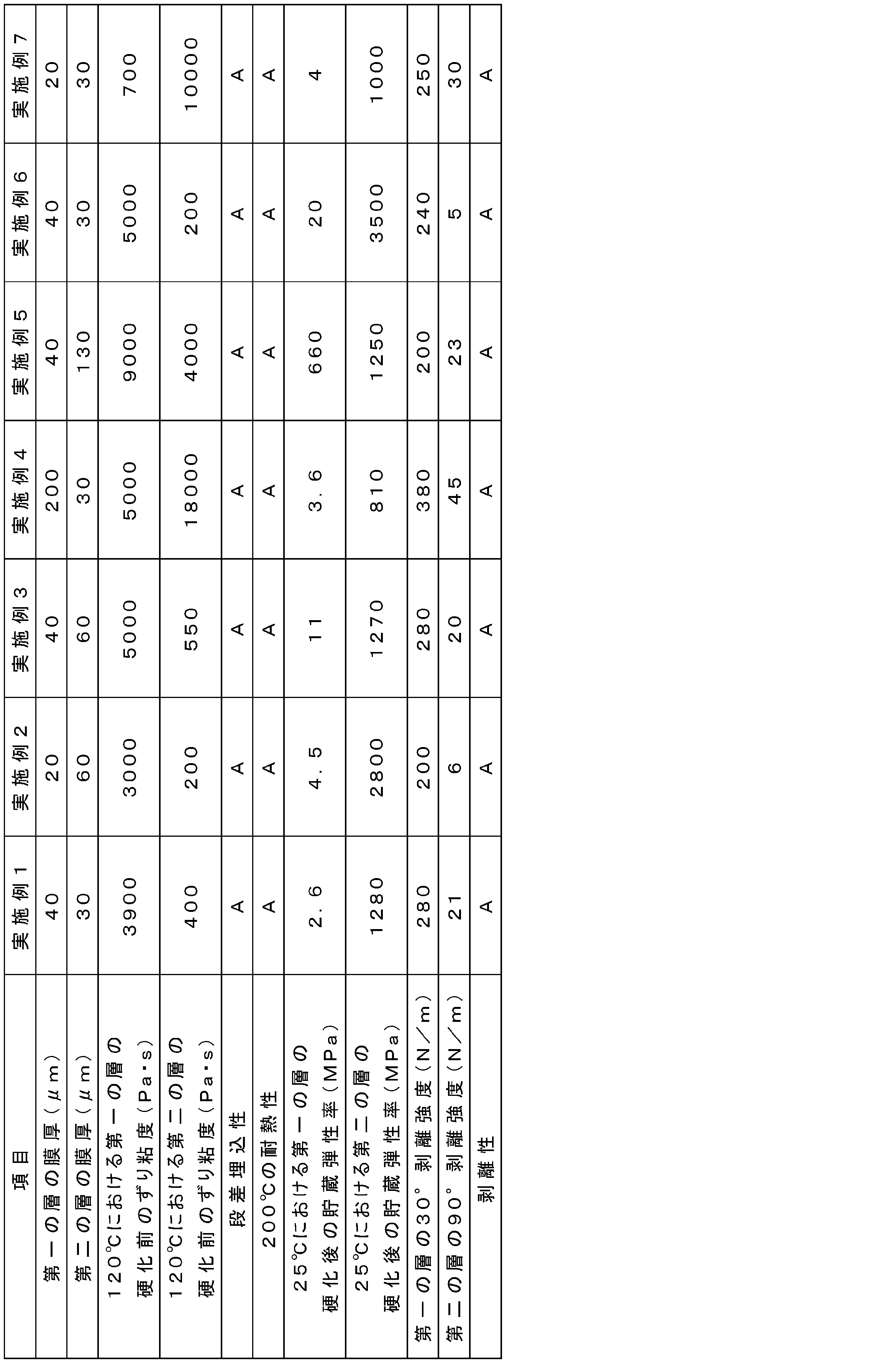

Claims (11)
- ガラス転移温度が-50℃~50℃である第一の熱可塑性樹脂を含む第一の層と、ガラス転移温度が-50℃~50℃である第二の熱可塑性樹脂及び硬化性成分を含む第二の層と、を備える、仮固定用樹脂フィルム。
- 前記第二の層における前記硬化性成分の含有量が、前記第二の熱可塑性樹脂100質量部に対して10~500質量部である、請求項1に記載の仮固定用樹脂フィルム。
- 前記第一の層の厚さが10~350μmであり、前記第二の層の厚さが10~350μmである、請求項1又は2に記載の仮固定用樹脂フィルム。
- 前記第一の層の厚さ及び前記第二の層の厚さが下記式(1)の関係を満たす、請求項1~3のいずれか一項に記載の仮固定用樹脂フィルム。
(1/10)a≦b≦10a・・・(1)
[式(1)中、aは第一の層の厚さを表し、bは第二の層の厚さを表す。] - 前記第一の熱可塑性樹脂が、架橋性官能基を有し、且つ、重量平均分子量が10万~120万の熱可塑性樹脂である、請求項1~4のいずれか一項に記載の仮固定用樹脂フィルム。
- 前記第二の熱可塑性樹脂が、架橋性官能基を有し、且つ、重量平均分子量が10万~120万の熱可塑性樹脂である、請求項1~5のいずれか一項に記載の仮固定用樹脂フィルム。
- 前記硬化性成分が熱硬化性樹脂である、請求項1~6のいずれか一項に記載の仮固定用樹脂フィルム。
- 前記第一の層がシリコーン化合物を更に含む、請求項1~7のいずれか一項に記載の仮固定用樹脂フィルム。
- 前記第二の層がシリコーン化合物を更に含む、請求項1~8のいずれか一項に記載の仮固定用樹脂フィルム。
- 前記第一の層が硬化促進剤を更に含む、請求項1~9のいずれか一項に記載の仮固定用樹脂フィルム。
- 前記第二の層が硬化促進剤を更に含む、請求項1~10のいずれか一項に記載の仮固定用樹脂フィルム。
Priority Applications (2)
| Application Number | Priority Date | Filing Date | Title |
|---|---|---|---|
| JP2018515721A JP6926070B2 (ja) | 2016-05-02 | 2017-04-28 | 仮固定用樹脂フィルム |
| KR1020187030733A KR102239644B1 (ko) | 2016-05-02 | 2017-04-28 | 가고정용 수지 필름 |
Applications Claiming Priority (2)
| Application Number | Priority Date | Filing Date | Title |
|---|---|---|---|
| JP2016092662 | 2016-05-02 | ||
| JP2016-092662 | 2016-05-02 |
Publications (1)
| Publication Number | Publication Date |
|---|---|
| WO2017191815A1 true WO2017191815A1 (ja) | 2017-11-09 |
Family
ID=60202972
Family Applications (1)
| Application Number | Title | Priority Date | Filing Date |
|---|---|---|---|
| PCT/JP2017/016978 Ceased WO2017191815A1 (ja) | 2016-05-02 | 2017-04-28 | 仮固定用樹脂フィルム |
Country Status (4)
| Country | Link |
|---|---|
| JP (2) | JP6926070B2 (ja) |
| KR (1) | KR102239644B1 (ja) |
| TW (1) | TWI720190B (ja) |
| WO (1) | WO2017191815A1 (ja) |
Cited By (11)
| Publication number | Priority date | Publication date | Assignee | Title |
|---|---|---|---|---|
| JP2019099664A (ja) * | 2017-11-30 | 2019-06-24 | 日本カーバイド工業株式会社 | 保護フィルム用粘着剤組成物及び保護フィルム |
| JP2019114599A (ja) * | 2017-12-21 | 2019-07-11 | 日立化成株式会社 | 仮固定用樹脂フィルム、仮固定用樹脂フィルムシート、及び半導体装置の製造方法 |
| WO2020129917A1 (ja) * | 2018-12-20 | 2020-06-25 | 日立化成株式会社 | 仮固定用樹脂組成物、仮固定用樹脂フィルム及び仮固定用シート並びに半導体装置の製造方法 |
| JP2020105276A (ja) * | 2018-12-26 | 2020-07-09 | 東京応化工業株式会社 | 接着剤組成物、積層体、積層体の製造方法、及び電子部品の製造方法 |
| WO2021006311A1 (ja) * | 2019-07-11 | 2021-01-14 | 信越化学工業株式会社 | 基板加工用仮接着材料及び積層体の製造方法 |
| WO2021095302A1 (ja) * | 2019-11-15 | 2021-05-20 | 昭和電工マテリアルズ株式会社 | 半導体装置の製造方法、並びにダイシング・ダイボンディング一体型フィルム及びその製造方法 |
| JPWO2021112070A1 (ja) * | 2019-12-02 | 2021-06-10 | ||
| JP2021129061A (ja) * | 2020-02-17 | 2021-09-02 | 力成科技股▲分▼有限公司 | 半導体製造装置および製造方法 |
| JPWO2021220929A1 (ja) * | 2020-04-30 | 2021-11-04 | ||
| JP2023034264A (ja) * | 2021-08-30 | 2023-03-13 | 日本ゼオン株式会社 | 複合ガラスシート及びその製造方法、並びに複合保護フィルム積層体 |
| WO2026058939A1 (ja) * | 2024-09-13 | 2026-03-19 | 株式会社レゾナック | フィルム状接着剤、ダイシング・ダイボンディング一体型フィルム、並びに半導体装置及びその製造方法 |
Families Citing this family (5)
| Publication number | Priority date | Publication date | Assignee | Title |
|---|---|---|---|---|
| US11767453B2 (en) * | 2018-12-31 | 2023-09-26 | Samsung Sdi Co., Ltd. | Silicone-based adhesive protective film and optical member comprising the same |
| KR102662018B1 (ko) * | 2019-10-31 | 2024-04-30 | 가부시끼가이샤 레조낙 | 가고정용 수지 조성물, 기판 반송용 서포트 테이프 및 전자 기기 장치의 제조 방법 |
| JP7771556B2 (ja) * | 2021-08-05 | 2025-11-18 | 三菱ケミカル株式会社 | フィルム、離型フィルム付きフィルム、振動板、積層体、成形品及び音響変換器 |
| JP2023101236A (ja) * | 2022-01-07 | 2023-07-20 | 株式会社レゾナック | 仮固定材形成用樹脂組成物、仮固定材、基板搬送用サポートテープ及び電子機器装置の製造方法 |
| CN119301740A (zh) * | 2022-06-02 | 2025-01-10 | 日产化学株式会社 | 光照射剥离用的粘接剂组合物、层叠体以及经加工的半导体基板的制造方法 |
Citations (5)
| Publication number | Priority date | Publication date | Assignee | Title |
|---|---|---|---|---|
| WO2014092200A1 (ja) * | 2012-12-14 | 2014-06-19 | リンテック株式会社 | 保護膜形成用フィルム |
| JP2014154704A (ja) * | 2013-02-08 | 2014-08-25 | Hitachi Chemical Co Ltd | ダイシング・ダイボンディング一体型テープ |
| JP2015135898A (ja) * | 2014-01-17 | 2015-07-27 | 日立化成株式会社 | 研削された基材の製造方法、並びにこれに用いられるフィルム状粘着剤及び積層体 |
| JP2016146437A (ja) * | 2015-02-09 | 2016-08-12 | 積水化学工業株式会社 | ウエハの処理方法 |
| WO2016140248A1 (ja) * | 2015-03-04 | 2016-09-09 | リンテック株式会社 | フィルム状接着剤複合シート及び半導体装置の製造方法 |
Family Cites Families (9)
| Publication number | Priority date | Publication date | Assignee | Title |
|---|---|---|---|---|
| JPS4936667B1 (ja) | 1969-12-19 | 1974-10-02 | ||
| JP2003147300A (ja) * | 2001-11-12 | 2003-05-21 | Lintec Corp | ウエハ裏面研削時の表面保護シートおよび半導体チップの製造方法 |
| JP4565804B2 (ja) | 2002-06-03 | 2010-10-20 | スリーエム イノベイティブ プロパティズ カンパニー | 被研削基材を含む積層体、その製造方法並びに積層体を用いた極薄基材の製造方法及びそのための装置 |
| JP2005019759A (ja) * | 2003-06-27 | 2005-01-20 | Mitsui Chemicals Inc | 半導体ウェハ表面保護用粘着フィルム及び該粘着フィルムを用いる半導体ウェハ保護方法 |
| JP2010238852A (ja) * | 2009-03-31 | 2010-10-21 | Mitsui Chemicals Inc | 半導体製造用テープおよび半導体装置の製造方法 |
| JP2011054940A (ja) * | 2009-08-07 | 2011-03-17 | Nitto Denko Corp | 半導体ウェハ保持保護用粘着シート及び半導体ウェハの裏面研削方法 |
| US8980985B2 (en) * | 2009-12-24 | 2015-03-17 | Three Bond Fine Chemical Co., Ltd. | Temporary fixing composition |
| WO2015079863A1 (ja) * | 2013-11-26 | 2015-06-04 | Jsr株式会社 | 積層体、基材の処理方法、仮固定用組成物および半導体装置 |
| CN105849215B (zh) * | 2013-12-26 | 2019-09-03 | 日立化成株式会社 | 临时固定用膜、临时固定用膜片材及半导体装置 |
-
2017
- 2017-04-28 WO PCT/JP2017/016978 patent/WO2017191815A1/ja not_active Ceased
- 2017-04-28 KR KR1020187030733A patent/KR102239644B1/ko active Active
- 2017-04-28 JP JP2018515721A patent/JP6926070B2/ja active Active
- 2017-04-28 TW TW106114301A patent/TWI720190B/zh active
-
2020
- 2020-05-21 JP JP2020088648A patent/JP6958674B2/ja active Active
Patent Citations (5)
| Publication number | Priority date | Publication date | Assignee | Title |
|---|---|---|---|---|
| WO2014092200A1 (ja) * | 2012-12-14 | 2014-06-19 | リンテック株式会社 | 保護膜形成用フィルム |
| JP2014154704A (ja) * | 2013-02-08 | 2014-08-25 | Hitachi Chemical Co Ltd | ダイシング・ダイボンディング一体型テープ |
| JP2015135898A (ja) * | 2014-01-17 | 2015-07-27 | 日立化成株式会社 | 研削された基材の製造方法、並びにこれに用いられるフィルム状粘着剤及び積層体 |
| JP2016146437A (ja) * | 2015-02-09 | 2016-08-12 | 積水化学工業株式会社 | ウエハの処理方法 |
| WO2016140248A1 (ja) * | 2015-03-04 | 2016-09-09 | リンテック株式会社 | フィルム状接着剤複合シート及び半導体装置の製造方法 |
Cited By (38)
| Publication number | Priority date | Publication date | Assignee | Title |
|---|---|---|---|---|
| JP2019099664A (ja) * | 2017-11-30 | 2019-06-24 | 日本カーバイド工業株式会社 | 保護フィルム用粘着剤組成物及び保護フィルム |
| JP2019114599A (ja) * | 2017-12-21 | 2019-07-11 | 日立化成株式会社 | 仮固定用樹脂フィルム、仮固定用樹脂フィルムシート、及び半導体装置の製造方法 |
| JP7147163B2 (ja) | 2017-12-21 | 2022-10-05 | 昭和電工マテリアルズ株式会社 | 仮固定用樹脂フィルム、仮固定用樹脂フィルムシート、及び半導体装置の製造方法 |
| US12094749B2 (en) | 2018-12-20 | 2024-09-17 | Resonac Corporation | Resin composition for temporary fixing use, resin film for temporary fixing use, sheet for temporary fixing use, and method for manufacturing semiconductor device |
| WO2020129917A1 (ja) * | 2018-12-20 | 2020-06-25 | 日立化成株式会社 | 仮固定用樹脂組成物、仮固定用樹脂フィルム及び仮固定用シート並びに半導体装置の製造方法 |
| JP7342886B2 (ja) | 2018-12-20 | 2023-09-12 | 株式会社レゾナック | 仮固定用樹脂組成物、仮固定用樹脂フィルム及び仮固定用シート並びに半導体装置の製造方法 |
| CN113195668B (zh) * | 2018-12-20 | 2023-01-13 | 昭和电工材料株式会社 | 临时固定用树脂组合物、临时固定用树脂膜及临时固定用片、以及半导体装置的制造方法 |
| JPWO2020129917A1 (ja) * | 2018-12-20 | 2021-11-04 | 昭和電工マテリアルズ株式会社 | 仮固定用樹脂組成物、仮固定用樹脂フィルム及び仮固定用シート並びに半導体装置の製造方法 |
| CN113195668A (zh) * | 2018-12-20 | 2021-07-30 | 昭和电工材料株式会社 | 临时固定用树脂组合物、临时固定用树脂膜及临时固定用片、以及半导体装置的制造方法 |
| JP2020105276A (ja) * | 2018-12-26 | 2020-07-09 | 東京応化工業株式会社 | 接着剤組成物、積層体、積層体の製造方法、及び電子部品の製造方法 |
| JP7221046B2 (ja) | 2018-12-26 | 2023-02-13 | 東京応化工業株式会社 | 接着剤組成物、積層体、積層体の製造方法、及び電子部品の製造方法 |
| JP2021014507A (ja) * | 2019-07-11 | 2021-02-12 | 信越化学工業株式会社 | 基板加工用仮接着材料及び積層体の製造方法 |
| JP7542089B2 (ja) | 2019-07-11 | 2024-08-29 | 信越化学工業株式会社 | 基板加工用仮接着材料及び積層体の製造方法 |
| JP7454922B2 (ja) | 2019-07-11 | 2024-03-25 | 信越化学工業株式会社 | 基板加工用仮接着材料及び積層体の製造方法 |
| CN114096633A (zh) * | 2019-07-11 | 2022-02-25 | 信越化学工业株式会社 | 基板加工用临时粘合材料及层叠体的制造方法 |
| KR20220032547A (ko) * | 2019-07-11 | 2022-03-15 | 신에쓰 가가꾸 고교 가부시끼가이샤 | 기판가공용 가접착재료 및 적층체의 제조방법 |
| KR102821921B1 (ko) * | 2019-07-11 | 2025-06-18 | 신에쓰 가가꾸 고교 가부시끼가이샤 | 기판가공용 가접착재료 및 적층체의 제조방법 |
| JP2023052354A (ja) * | 2019-07-11 | 2023-04-11 | 信越化学工業株式会社 | 基板加工用仮接着材料及び積層体の製造方法 |
| WO2021006311A1 (ja) * | 2019-07-11 | 2021-01-14 | 信越化学工業株式会社 | 基板加工用仮接着材料及び積層体の製造方法 |
| TWI862638B (zh) * | 2019-11-15 | 2024-11-21 | 日商力森諾科股份有限公司 | 半導體裝置的製造方法、以及切晶黏晶一體型膜及其製造方法 |
| JP7409029B2 (ja) | 2019-11-15 | 2024-01-09 | 株式会社レゾナック | 半導体装置の製造方法、並びにダイシング・ダイボンディング一体型フィルム及びその製造方法 |
| JP2021082648A (ja) * | 2019-11-15 | 2021-05-27 | 昭和電工マテリアルズ株式会社 | 半導体装置の製造方法、並びにダイシング・ダイボンディング一体型フィルム及びその製造方法 |
| WO2021095302A1 (ja) * | 2019-11-15 | 2021-05-20 | 昭和電工マテリアルズ株式会社 | 半導体装置の製造方法、並びにダイシング・ダイボンディング一体型フィルム及びその製造方法 |
| CN114868232A (zh) * | 2019-12-02 | 2022-08-05 | 信越化学工业株式会社 | 晶片加工用临时粘接剂、晶片层叠体及薄型晶片的制造方法 |
| WO2021112070A1 (ja) * | 2019-12-02 | 2021-06-10 | 信越化学工業株式会社 | ウエハ加工用仮接着剤、ウエハ積層体及び薄型ウエハの製造方法 |
| KR20220108799A (ko) * | 2019-12-02 | 2022-08-03 | 신에쓰 가가꾸 고교 가부시끼가이샤 | 웨이퍼 가공용 가접착제, 웨이퍼 적층체 및 박형 웨이퍼의 제조 방법 |
| KR102874851B1 (ko) * | 2019-12-02 | 2025-10-24 | 신에쓰 가가꾸 고교 가부시끼가이샤 | 웨이퍼 가공용 가접착제, 웨이퍼 적층체 및 박형 웨이퍼의 제조 방법 |
| JPWO2021112070A1 (ja) * | 2019-12-02 | 2021-06-10 | ||
| JP2024113159A (ja) * | 2019-12-02 | 2024-08-21 | 信越化学工業株式会社 | ウエハ加工用仮接着剤、ウエハ積層体及び薄型ウエハの製造方法 |
| JP7682807B2 (ja) | 2019-12-02 | 2025-05-26 | 信越化学工業株式会社 | ウエハ加工用仮接着剤、ウエハ積層体及び薄型ウエハの製造方法 |
| JP2021129061A (ja) * | 2020-02-17 | 2021-09-02 | 力成科技股▲分▼有限公司 | 半導体製造装置および製造方法 |
| JP7658367B2 (ja) | 2020-04-30 | 2025-04-08 | 信越化学工業株式会社 | ウエハ加工用仮接着剤、ウエハ積層体及び薄型ウエハの製造方法 |
| JPWO2021220929A1 (ja) * | 2020-04-30 | 2021-11-04 | ||
| US11970639B2 (en) | 2020-04-30 | 2024-04-30 | Shin-Etsu Chemical Co., Ltd. | Temporary adhesive for wafer processing, wafer laminate and method for producing thin wafer |
| WO2021220929A1 (ja) * | 2020-04-30 | 2021-11-04 | 信越化学工業株式会社 | ウエハ加工用仮接着剤、ウエハ積層体及び薄型ウエハの製造方法 |
| JP2023034264A (ja) * | 2021-08-30 | 2023-03-13 | 日本ゼオン株式会社 | 複合ガラスシート及びその製造方法、並びに複合保護フィルム積層体 |
| JP7746741B2 (ja) | 2021-08-30 | 2025-10-01 | 日本ゼオン株式会社 | 複合ガラスシート及びその製造方法、並びに複合保護フィルム積層体 |
| WO2026058939A1 (ja) * | 2024-09-13 | 2026-03-19 | 株式会社レゾナック | フィルム状接着剤、ダイシング・ダイボンディング一体型フィルム、並びに半導体装置及びその製造方法 |
Also Published As
| Publication number | Publication date |
|---|---|
| KR20180122460A (ko) | 2018-11-12 |
| KR102239644B1 (ko) | 2021-04-12 |
| JPWO2017191815A1 (ja) | 2018-11-08 |
| TW201806768A (zh) | 2018-03-01 |
| JP2020161823A (ja) | 2020-10-01 |
| TWI720190B (zh) | 2021-03-01 |
| JP6926070B2 (ja) | 2021-08-25 |
| JP6958674B2 (ja) | 2021-11-02 |
Similar Documents
| Publication | Publication Date | Title |
|---|---|---|
| JP6958674B2 (ja) | 電子部品の加工方法 | |
| JP6443343B2 (ja) | 仮固定用フィルム、仮固定用フィルムシート及び半導体装置 | |
| KR102899303B1 (ko) | 기판 반송용 서포트 테이프 및 전자 기기 장치의 제조 방법 | |
| JP7147163B2 (ja) | 仮固定用樹脂フィルム、仮固定用樹脂フィルムシート、及び半導体装置の製造方法 | |
| JP2018009138A (ja) | 仮固定用樹脂組成物、仮固定用樹脂フィルム及び仮固定用樹脂フィルムシート | |
| JP7342886B2 (ja) | 仮固定用樹脂組成物、仮固定用樹脂フィルム及び仮固定用シート並びに半導体装置の製造方法 | |
| JP2017204612A (ja) | 電子部品支持部材 | |
| JP2017203139A (ja) | 電子部品支持部材 | |
| JP2019151696A (ja) | 仮固定用の樹脂組成物、樹脂フィルム及び樹脂フィルムシート | |
| WO2016035821A1 (ja) | 仮固定用樹脂組成物、仮固定用樹脂フィルム、仮固定用樹脂フィルムシート及び半導体ウェハの加工方法 | |
| JP2017048266A (ja) | 半導体ウェハの仮固定用樹脂組成物及び半導体ウェハの加工方法 | |
| JP7392731B2 (ja) | 仮固定用樹脂組成物、基板搬送用サポートテープ及び電子機器装置の製造方法 | |
| JP6213252B2 (ja) | 研削された基材の製造方法、並びにこれに用いられるフィルム状粘着剤及び積層体 | |
| JP6958089B2 (ja) | 仮固定用樹脂フィルム、仮固定用樹脂フィルムシート及びそれらの製造方法 | |
| JP7392730B2 (ja) | 仮固定用樹脂組成物、基板搬送用サポートテープ及び電子機器装置の製造方法 | |
| JP2023101236A (ja) | 仮固定材形成用樹脂組成物、仮固定材、基板搬送用サポートテープ及び電子機器装置の製造方法 |
Legal Events
| Date | Code | Title | Description |
|---|---|---|---|
| ENP | Entry into the national phase |
Ref document number: 2018515721 Country of ref document: JP Kind code of ref document: A |
|
| ENP | Entry into the national phase |
Ref document number: 20187030733 Country of ref document: KR Kind code of ref document: A |
|
| NENP | Non-entry into the national phase |
Ref country code: DE |
|
| 121 | Ep: the epo has been informed by wipo that ep was designated in this application |
Ref document number: 17792748 Country of ref document: EP Kind code of ref document: A1 |
|
| 122 | Ep: pct application non-entry in european phase |
Ref document number: 17792748 Country of ref document: EP Kind code of ref document: A1 |