WO2017209051A1 - チャック、基板保持装置、パターン形成装置、及び物品の製造方法 - Google Patents
チャック、基板保持装置、パターン形成装置、及び物品の製造方法 Download PDFInfo
- Publication number
- WO2017209051A1 WO2017209051A1 PCT/JP2017/019917 JP2017019917W WO2017209051A1 WO 2017209051 A1 WO2017209051 A1 WO 2017209051A1 JP 2017019917 W JP2017019917 W JP 2017019917W WO 2017209051 A1 WO2017209051 A1 WO 2017209051A1
- Authority
- WO
- WIPO (PCT)
- Prior art keywords
- chuck
- substrate
- support
- portions
- support portion
- Prior art date
- Legal status (The legal status is an assumption and is not a legal conclusion. Google has not performed a legal analysis and makes no representation as to the accuracy of the status listed.)
- Ceased
Links
Images


Classifications
-
- H—ELECTRICITY
- H10—SEMICONDUCTOR DEVICES; ELECTRIC SOLID-STATE DEVICES NOT OTHERWISE PROVIDED FOR
- H10P—GENERIC PROCESSES OR APPARATUS FOR THE MANUFACTURE OR TREATMENT OF DEVICES COVERED BY CLASS H10
- H10P72/00—Handling or holding of wafers, substrates or devices during manufacture or treatment thereof
- H10P72/70—Handling or holding of wafers, substrates or devices during manufacture or treatment thereof for supporting or gripping
- H10P72/76—Handling or holding of wafers, substrates or devices during manufacture or treatment thereof for supporting or gripping using mechanical means, e.g. clamps or pinches
- H10P72/7604—Handling or holding of wafers, substrates or devices during manufacture or treatment thereof for supporting or gripping using mechanical means, e.g. clamps or pinches the wafers being placed on a susceptor, stage or support
-
- G—PHYSICS
- G03—PHOTOGRAPHY; CINEMATOGRAPHY; ANALOGOUS TECHNIQUES USING WAVES OTHER THAN OPTICAL WAVES; ELECTROGRAPHY; HOLOGRAPHY
- G03F—PHOTOMECHANICAL PRODUCTION OF TEXTURED OR PATTERNED SURFACES, e.g. FOR PRINTING, FOR PROCESSING OF SEMICONDUCTOR DEVICES; MATERIALS THEREFOR; ORIGINALS THEREFOR; APPARATUS SPECIALLY ADAPTED THEREFOR
- G03F7/00—Photomechanical, e.g. photolithographic, production of textured or patterned surfaces, e.g. printing surfaces; Materials therefor, e.g. comprising photoresists; Apparatus specially adapted therefor
- G03F7/70—Microphotolithographic exposure; Apparatus therefor
- G03F7/70691—Handling of masks or workpieces
- G03F7/707—Chucks, e.g. chucking or un-chucking operations or structural details
-
- G—PHYSICS
- G03—PHOTOGRAPHY; CINEMATOGRAPHY; ANALOGOUS TECHNIQUES USING WAVES OTHER THAN OPTICAL WAVES; ELECTROGRAPHY; HOLOGRAPHY
- G03F—PHOTOMECHANICAL PRODUCTION OF TEXTURED OR PATTERNED SURFACES, e.g. FOR PRINTING, FOR PROCESSING OF SEMICONDUCTOR DEVICES; MATERIALS THEREFOR; ORIGINALS THEREFOR; APPARATUS SPECIALLY ADAPTED THEREFOR
- G03F7/00—Photomechanical, e.g. photolithographic, production of textured or patterned surfaces, e.g. printing surfaces; Materials therefor, e.g. comprising photoresists; Apparatus specially adapted therefor
- G03F7/20—Exposure; Apparatus therefor
-
- H—ELECTRICITY
- H10—SEMICONDUCTOR DEVICES; ELECTRIC SOLID-STATE DEVICES NOT OTHERWISE PROVIDED FOR
- H10P—GENERIC PROCESSES OR APPARATUS FOR THE MANUFACTURE OR TREATMENT OF DEVICES COVERED BY CLASS H10
- H10P72/00—Handling or holding of wafers, substrates or devices during manufacture or treatment thereof
- H10P72/70—Handling or holding of wafers, substrates or devices during manufacture or treatment thereof for supporting or gripping
- H10P72/76—Handling or holding of wafers, substrates or devices during manufacture or treatment thereof for supporting or gripping using mechanical means, e.g. clamps or pinches
- H10P72/7604—Handling or holding of wafers, substrates or devices during manufacture or treatment thereof for supporting or gripping using mechanical means, e.g. clamps or pinches the wafers being placed on a susceptor, stage or support
- H10P72/7611—Handling or holding of wafers, substrates or devices during manufacture or treatment thereof for supporting or gripping using mechanical means, e.g. clamps or pinches the wafers being placed on a susceptor, stage or support characterised by edge profile or support profile
-
- H—ELECTRICITY
- H10—SEMICONDUCTOR DEVICES; ELECTRIC SOLID-STATE DEVICES NOT OTHERWISE PROVIDED FOR
- H10P—GENERIC PROCESSES OR APPARATUS FOR THE MANUFACTURE OR TREATMENT OF DEVICES COVERED BY CLASS H10
- H10P72/00—Handling or holding of wafers, substrates or devices during manufacture or treatment thereof
- H10P72/70—Handling or holding of wafers, substrates or devices during manufacture or treatment thereof for supporting or gripping
- H10P72/76—Handling or holding of wafers, substrates or devices during manufacture or treatment thereof for supporting or gripping using mechanical means, e.g. clamps or pinches
- H10P72/7604—Handling or holding of wafers, substrates or devices during manufacture or treatment thereof for supporting or gripping using mechanical means, e.g. clamps or pinches the wafers being placed on a susceptor, stage or support
- H10P72/7614—Handling or holding of wafers, substrates or devices during manufacture or treatment thereof for supporting or gripping using mechanical means, e.g. clamps or pinches the wafers being placed on a susceptor, stage or support characterised by a plurality of individual support members, e.g. support posts or protrusions
-
- H—ELECTRICITY
- H10—SEMICONDUCTOR DEVICES; ELECTRIC SOLID-STATE DEVICES NOT OTHERWISE PROVIDED FOR
- H10P—GENERIC PROCESSES OR APPARATUS FOR THE MANUFACTURE OR TREATMENT OF DEVICES COVERED BY CLASS H10
- H10P72/00—Handling or holding of wafers, substrates or devices during manufacture or treatment thereof
- H10P72/70—Handling or holding of wafers, substrates or devices during manufacture or treatment thereof for supporting or gripping
- H10P72/76—Handling or holding of wafers, substrates or devices during manufacture or treatment thereof for supporting or gripping using mechanical means, e.g. clamps or pinches
- H10P72/7604—Handling or holding of wafers, substrates or devices during manufacture or treatment thereof for supporting or gripping using mechanical means, e.g. clamps or pinches the wafers being placed on a susceptor, stage or support
- H10P72/7624—Handling or holding of wafers, substrates or devices during manufacture or treatment thereof for supporting or gripping using mechanical means, e.g. clamps or pinches the wafers being placed on a susceptor, stage or support characterised by the mechanical construction of the susceptor, stage or support
-
- H—ELECTRICITY
- H10—SEMICONDUCTOR DEVICES; ELECTRIC SOLID-STATE DEVICES NOT OTHERWISE PROVIDED FOR
- H10P—GENERIC PROCESSES OR APPARATUS FOR THE MANUFACTURE OR TREATMENT OF DEVICES COVERED BY CLASS H10
- H10P72/00—Handling or holding of wafers, substrates or devices during manufacture or treatment thereof
- H10P72/70—Handling or holding of wafers, substrates or devices during manufacture or treatment thereof for supporting or gripping
- H10P72/78—Handling or holding of wafers, substrates or devices during manufacture or treatment thereof for supporting or gripping using vacuum or suction, e.g. Bernoulli chucks
Definitions
- the present invention relates to a chuck, a substrate holding device, a pattern forming device, and an article manufacturing method.
- Patent Document 1 describes a configuration in which the upper surface of a chuck is partitioned into a plurality of rectangular sections by a support portion having two convex portions and a concave portion therebetween. Correcting the flatness of the substrate by controlling the gas supply / exhaust amount into each rectangular section according to the measurement result of the flatness of the held substrate while exhausting the recess and holding the substrate. Is described.
- a substrate having a thinner thickness than before has been increasingly used.
- the flatness of the surface of the substrate may be deteriorated by the contact between the chuck and the substrate.
- an object of the present invention is to provide a chuck, a substrate holding device, and a lithography apparatus that can improve the flatness of the substrate in a state where the substrate is held.
- a chuck includes first and second support portions each having a repetitive structure of a convex portion and a concave portion on a base portion, wherein the convex portion is in contact with a substrate, and the first support portion is provided. And a chuck that holds the substrate by exhausting the recess so that the recess has a negative pressure with respect to a space between the second support and the first support and the second support. At least one of the support portions has at least four protrusions and three recesses.
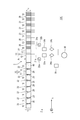
- FIG. 1 is a view of the chuck 1 as viewed from the + Z direction
- FIG. 2 is a view showing the configuration of the holding device 100 and includes a cross-sectional view taken along the line AA of the chuck 1.
- FIG. 3 is an enlarged view of the region 40 of FIG.
- the holding device 100 includes a chuck 1, an exhaust unit 30, and a pipe 31.
- the exhaust unit 30 exhausts the support unit 10 on the chuck 1, the chuck 1 sucks and holds the placed substrate.
- Three openings 30 are formed in the surface 2 of the chuck 1 that holds the substrate.
- the opening 30 is for a support pin (not shown) for temporarily supporting the substrate to protrude from the base portion 14 having the surface 2 when the substrate is carried into and out of the holding device 100.
- the chuck 1 is provided with support portions 10 protruding from the surface 2 and regions 20 alternately and concentrically.
- Each support portion 10 has four convex portions (contact portions) 11 that can come into contact with the substrate and three concave portions 13, and supports the concave portions 13 between two adjacent convex portions 11.
- the part is composed.
- the support portion 10 has a structure in which four convex portions 11 and three concave portions 13 are arranged in a direction (one direction) from the center of the chuck 1 toward the outer periphery of the chuck 1.
- the recesses 13 are continuously arranged in the direction toward the outer periphery (formed continuously without the region 20).
- the widths of the three recesses 13 can be arbitrarily set. For example, as shown in FIG. 3, the width b of the center recess 13 is wider than the widths a and c of the recesses 13 (other recesses) at both ends. It is preferable. Thereby, the deformation
- Each recess 13 has at least one opening 12, and at least three recesses 12 included in one support 10 are connected to a common exhaust 30. That is, the opening 12 is a common opening for the three recesses 13. In the present embodiment, all the openings 12 are connected to the common exhaust part 30.
- An exhaust part 30 for exhausting the recess 13 is provided via the opening 12 and the pipe 31.
- the exhaust unit 30 is, for example, a vacuum pump.
- the region 20 is a region between the support unit 10 and the support unit 10, and at least one opening 22 is provided in each region 20.
- the opening 22 is an opening through which a gas (such as air) in the atmosphere in which the chuck 1 is disposed can enter and exit.
- a gas such as air
- region 20 which is the side part space of the support part 10 (space between a 1st support part and a 2nd support part).
- the opening 22 may be connected to a gas supply portion that supplies a predetermined gas, or the pressure is adjusted. Gas may be supplied.
- the holding device 100 holds the unloaded substrate. Since the support portion 10 has a structure in which the four convex portions 11 and the concave portions 13 provided between the respective convex portions 11 are arranged in one direction, the flatness of the substrate in a state where the substrate is held can be obtained. Can be improved. In particular, even when the substrate is thin, the substrate can be held while maintaining high flatness.
- the chuck 1 is suitable for holding a special substrate that has been excavated, for example, until the thickness of the central portion becomes about 1/10 of the outer peripheral portion.
- Example 1 An example in which the substrate is held by the chuck 1 will be described using a comparative example.
- FIG. 4 is a cross-sectional view of the chuck 95, which is different from the chuck 1 in that the support portions 90 arranged at equal intervals have two convex portions 91 and one concave portion 93 therebetween.
- the support portion 90 is arranged concentrically like the chuck 1 when the chuck 95 is viewed from the + Z direction.
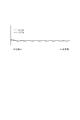
- FIG. 5A is a diagram showing a simulation result of the flatness of the substrate when the substrate is held using the chuck 95 according to the comparative example.
- FIG. 5B is a diagram showing a simulation result of the flatness of the substrate when the substrate is held using the chuck 1.
- the vertical axis represents the position in the height direction of the back surface of the substrate held by each chuck
- the horizontal axis represents the position in the radial direction of the chuck.
- the left end point of the horizontal axis is the center position of the chuck 1, and the right end point of the horizontal axis is the outer peripheral position.
- each chuck has eight support portions 10 or support portions 90.
- the other part of the inner part of the support part 90 closest to the center of the chuck 95 and the outer part of the support part 90 closest to the outer periphery of the chuck 95 In comparison, the position of the back side of the substrate was greatly raised. That is, the portion on the center side of the substrate and the portion on the outer peripheral side of the substrate are greatly deformed as compared with the other portions. Further, the position of the back surface of the substrate was also raised locally between the support portion 90 and the support portion 90.
- the substrate can be held with a flatness of 1/10 or less in the case of the chuck 1 compared to the case of the chuck 95. That is, the support 10 has a structure in which the four protrusions 11 and the recesses 13 provided between the protrusions 11 are arranged in one direction, whereby the plane of the substrate in a state where the substrate is held. It was confirmed that the degree could be improved.
- FIG. 6 is an enlarged view of a cross section of the chuck 1 according to the second embodiment.
- the same members as those in the first embodiment are denoted by the same reference numerals, and detailed description thereof is omitted.
- the chuck 1 according to the present embodiment is a support portion 10 in which one support portion 10 includes three recesses 13, and the other support portion 90 is a support portion having one recess 93. In this way, even if all the support portions that support the substrate do not have the three recessed portions 13 as in the support portion 10, at least one of the plurality of support portions has the three recessed portions 13. It only has to have. Even in the case of the present embodiment, the same effects as those of the first embodiment are obtained.
- the support portion closest to the center position P0 of the chuck 1 is preferably the support portion 10.
- FIG. 7 is a simulation result showing the position of the back surface of the substrate held by the chuck 1 according to the second embodiment. Except for changing the configuration of the chuck 1, the various conditions of the simulation and the configuration of the shaft are the same as described above, and thus detailed description thereof is omitted.
- the support portion 10 is disposed at a position closest to the center of the chuck 1, the deformation of the substrate in the central portion of the substrate, which has been noticeable in the comparative example described above, can be significantly reduced. I was able to. The substrate can be held with good flatness.
- the support portion closest to the center of the chuck 1 may be the support portion 10.
- the flatness of the substrate in a state where the substrate is held can be improved by using the support portion closest to the center of the chuck 1 and the support portion closest to the outer periphery of the chuck 1 as the support portion 10.
- FIG. 8 is a diagram illustrating a configuration of the holding device 300 according to the third embodiment, and includes a cross-sectional view of the chuck 1.
- the same members as those in the first embodiment are denoted by the same reference numerals, and detailed description thereof is omitted.
- the holding device 300 controls the evacuation means by the control unit 35, the adsorption pressure generated at the support unit 10 (part of the support unit) closest to the center position P 0 of the chuck 1, and the substrate generated at the other support units 10.
- the adsorption pressure is controlled individually.
- the holding device 300 includes an exhaust part 30, pipes 31a and 31b, pressure gauges 32a and 32b, electromagnetic valves 33a and 33b, and adjustment parts 34a and 34b as exhaust means.
- the pressure gauge 32a measures the pressure in the pipe 31a
- the pressure gauge 32b measures the pressure in the pipe 31b.
- the solenoid valve 33a switches ON / OFF of the exhaust of the pipe 31a
- the solenoid valve 33b switches ON / OFF of the exhaust of the pipe 31b.
- the adjusting unit 34a adjusts the pressure in the pipe 31a
- the adjusting unit 34b adjusts the pressure in the pipe 31a.
- the control unit 35 controls the electromagnetic valves 33a and 33b and the adjustment units 34a and 34b.
- control unit 35 controls the adjustment unit 34b so as to keep the inside of the pipe 31b at a predetermined pressure and variably controls only the pressure in the pipe 31a.
- FIG. 9 is a simulation result showing the position of the back surface of the substrate held by the chuck 1 according to the third embodiment.
- various simulation conditions and the configuration of the shaft are the same as described above, and thus detailed description thereof is omitted.
- the control unit 35 controls the pressure in the pipe 31a based on the flatness information at the center of the substrate.
- the solid line indicates the position in the height direction of the back surface of the substrate when the substrate is held at an adsorption pressure of 75 kPa in all the support portions 10.
- the broken line indicates the position in the height direction of the back surface of the substrate when the suction pressure generated at the support portion 10 closest to the center position P0 of the chuck 1 is reduced to 40 kPa.
- the suction force at the first support portion it is preferable to previously set the suction force at the first support portion to 75 kPa.
- the position of the back surface can be raised in advance as compared with the outer peripheral portion, and the flatness of the surface of the substrate can be increased.
- the holding device 300 has the same effect as that of the first embodiment. Furthermore, by controlling the position of the back surface of the substrate by controlling the pressure of the pipe 31a, it is possible to compensate for the deterioration in flatness due to the thickness distribution of the substrate.
- the controller 35 may acquire the flatness information based on the result of the thickness measurement using another measuring instrument before being carried into the holding device 300, or after being carried into the holding device 300.
- Flatness information may be acquired by measuring the position of the surface of the substrate using ultrasonic waves or light. Or you may acquire the information input from the user as flatness information of a board
- the control of the adsorption pressure by the control unit 35 includes ON / OFF of the exhaust by controlling the electromagnetic valves 33a and 33b.
- the piping 31b may also control the adsorption pressure continuously.
- FIG. 10 is an enlarged view when the chuck 1 according to the fourth embodiment is viewed from the + Z direction, and illustrates a portion including one support portion 10.
- the same members as those in the first embodiment are denoted by the same reference numerals, and detailed description thereof is omitted. Further, the three recesses 13 may be exhausted by one opening 12.
- the support portion 10 may have a structure in which the three convex portions 11 and the two concave portions 13 are arranged in one direction. Good.
- the one or more support portions 10 have a structure in which three convex portions 11 and two concave portions 13 are arranged in one direction.
- the support part 10 may be the support part 10 except for the support part closest to the center of the chuck 1 and the support part closest to the outer periphery of the chuck 1. .
- the flatness of the substrate in a state where the substrate is held can be improved as compared with the case of the chuck 95.
- FIG. 11 is a diagram showing a configuration of an exposure apparatus 600 as the lithography apparatus.
- An axis parallel to the optical axis of the projection optical system 604 (vertical direction in this embodiment) is taken as the Z axis.
- the directions perpendicular to each other in a plane perpendicular to the Z axis are taken as an X axis and a Y axis.
- the exposure apparatus 600 illuminates a reticle (original) 602 with illumination light 603 via an illumination optical system 601, and projects an image of a pattern formed on the illuminated reticle 602 onto a substrate 605 via a projection optical system 604. To do.
- the stage 606 holds the reticle 602 and scans in the X-axis direction.
- the stage 607 moves the chuck 1 and the substrate 605 held by the chuck 1 by a drive mechanism (not shown) such as a linear motor.
- the exposure apparatus 600 forms a latent image pattern on the resist applied to the substrate 605 while relatively scanning the reticle 602 and the substrate 605 with the stages 606 and 607.
- the interferometer 608 irradiates the mirror 609 with the laser light and the interferometer 610 irradiates the mirror 611 with laser light, and receives the reflected light to detect the position of the reticle 602 and the substrate 605.
- the detection system 612 detects an alignment mark (not shown) formed on the substrate 605 and a reference mark (not shown) provided on the stage 607.
- the holding device 100 includes a top plate 614 having a built-in pin 613 that supports the substrate 605 when the substrate 605 is carried in and out, and a lifting mechanism (not configured) that moves the chuck 1 and the top plate 614 up and down with respect to the pin 613. As shown).
- the control unit 615 is connected to the stages 606 and 607, the detection system 612, the interferometers 608 and 610, and the holding device 100, and comprehensively controls them. For example, at the time of exposure processing, a pattern formation position is determined based on the detection result of the detection system 612, and the stages 606 and 607 are controlled based on position information obtained from the interferometers 608 and 610.
- the controller 615 controls the lifting mechanism of the holding device 100 and the movement of the stage 607 when the substrate 605 is carried in and out.
- the control unit 615 may be configured in a casing that accommodates components other than the control unit 615, or may be configured in a casing different from the casing.
- the flatness of the substrate 605 can be improved as compared with the case of holding with a holding device using a supporting member that does not have the three concave portions 13. Therefore, it becomes easy to perform exposure while aligning the position of the surface of the substrate 605 with the focus position of the exposure light 616. Thereby, degradation of the resolution line width of the pattern formed on the substrate 605, which may occur when the flatness of the substrate 605 is poor, can be reduced.
- the chuck 1 and the holding apparatuses 100 and 300 according to the second to fifth embodiments may be mounted.
- Light that the exposure apparatus 600 irradiates the substrate 605 is not limited to i-line (wavelength 365 nm), but light in the far ultraviolet region such as KrF light (wavelength 248 nm) and ArF light (wavelength 193 nm), g-line. Light in the visible light region such as (wavelength 436 nm) may be used.
- the lithography apparatus according to the embodiment of the present invention may be an apparatus that forms a resist (imprint material) pattern on a substrate by an imprint method, or the substrate is irradiated with a laser beam or a charged particle beam to be latent on the wafer. An apparatus for drawing an image pattern may be used.
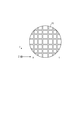
- the shape of the support portion 10 of the chuck 1 does not necessarily have to be a continuous circle (annular). A single rectangle (rectangular ring) may be used.
- FIG. 1 shows a case where the support portions 10 are concentric, that is, a plurality of annular support portions 10 are arranged in multiple directions along the substrate held by the chuck 1, Also good.
- the shape of the support part 10 may be a combination of a linear support part 10 or a linear support part 10 that partitions the surface 2 into a plurality of rectangular regions, as shown in FIG. A combination of the linear support portion 10 and the annular support portion 10 may be used.
- illustration of the recessed part 13 and the opening 12 contained in the support part 10 is abbreviate
- the support portions 10 may be arranged so as to be multiplexed along the surface of the substrate held by the chuck 1.
- the support portion 10 may be integrally formed with the base portion 14 constituting the surface 2 or may be provided separately from the base portion 14.
- the height of the bottom of the recess 13 may be the same height as the surface 2 or higher than the surface 2.
- the third embodiment may be appropriately combined with the chuck 1 shown in the other embodiments.
- the arrangement of the openings 12 shown in the fourth embodiment may be implemented in combination with the chuck 1 shown in other embodiments as appropriate.
- a pattern formed on a substrate using a lithography apparatus is temporarily used when various articles are manufactured.
- the article is an electric circuit element, an optical element, a MEMS, a recording element, a sensor, or a mold.
- the electric circuit elements include volatile or nonvolatile semiconductor memories such as DRAM, SRAM, flash memory, and MRAM, and semiconductor elements such as LSI, CCD, image sensor, and FPGA.
- the mold include an imprint mold.
- the pattern formed using the lithography apparatus is subjected to etching or ion implantation in the substrate processing step, and then the resist used as a mask is removed.
- the resist is developed before the above-described processing steps.
- the resist cured pattern formed by using an imprint apparatus as a lithography apparatus may be used as a constituent member of at least a part of the article.
Landscapes
- Physics & Mathematics (AREA)
- General Physics & Mathematics (AREA)
- Container, Conveyance, Adherence, Positioning, Of Wafer (AREA)
- Exposure And Positioning Against Photoresist Photosensitive Materials (AREA)
- Shaping Of Tube Ends By Bending Or Straightening (AREA)
Abstract
本発明の実施形態に係るチャックは、基部上に、凸部11と凹部13との繰り返し構造をそれぞれ有する第1及び第2支持部10を備え、凸部11が基板と当接し、第1支持部10及び前記第2支持部10の間の空間に対して凹部13が負圧になるように凹部13が排気されることで基板を保持するチャックであって、第1支持部10および第2支持部10のうち少なくとも一方の支持部は、少なくとも4つの凸部11と3つの凹部13を有することを特徴とする。
Description
本発明は、チャック、基板保持装置、パターン形成装置、及び物品の製造方法に関する。
リソグラフィ装置等に搭載される基板保持装置において、露光光のフォーカス位置を精度良く合わせるために、基板の平面度を良好に保つ必要がある。
特許文献1には、チャック上面を、2つの凸部とその間の凹部とを備えた支持部によって複数の矩形区画に仕切られた構成が記載されている。凹部を排気して基板を保持しつつ、保持された基板の平面度の計測結果に応じて各矩形区画内への気体の給排気量を制御することにより、該基板の平面度を矯正することが記載されている。
従来よりも厚さの薄い基板が使用されることが多くなってきている。排気によって基板を保持する際に、基板の裏面と当接する部分のチャックの構造によっては、チャックと基板の当接によって基板の表面の平面度を悪化させてしまう恐れがある。
そこで、本発明は、基板を保持した状態における該基板の平面度を向上することができるチャック、基板保持装置、リソグラフィ装置を提供することを目的とする。
本発明の一実施形態にかかるチャックは、基部上に、凸部と凹部との繰り返し構造をそれぞれ有する第1及び第2支持部を備え、前記凸部が基板と当接し、前記第1支持部及び前記第2支持部の間の空間に対して前記凹部が負圧になるように前記凹部が排気されることで前記基板を保持するチャックであって、前記第1支持部および前記第2支持部のうち少なくとも一方の支持部は、少なくとも4つの前記凸部と3つの凹部を有することを特徴とする。
[第1実施形態]
図1、図2、図3を用いて第1実施形態に係るチャック1および基板を保持する保持装置(基板保持装置)100の構成を説明する。チャック1に保持される基板の表面に沿う方向に対して垂直な方向の軸をZ軸、該Z軸に垂直な平面内において互に直交する方向をX軸およびY軸とする。図1はチャック1を+Z方向から見た図であり、図2は保持装置100の構成を示す図であって、チャック1のA-A断面図を含んでいる。図3は図2の領域40の拡大図である。
図1、図2、図3を用いて第1実施形態に係るチャック1および基板を保持する保持装置(基板保持装置)100の構成を説明する。チャック1に保持される基板の表面に沿う方向に対して垂直な方向の軸をZ軸、該Z軸に垂直な平面内において互に直交する方向をX軸およびY軸とする。図1はチャック1を+Z方向から見た図であり、図2は保持装置100の構成を示す図であって、チャック1のA-A断面図を含んでいる。図3は図2の領域40の拡大図である。
保持装置100はチャック1、排気部30、および配管31を有する。排気部30によってチャック1上の支持部10で排気が行われることで、チャック1は載置された基板を吸着保持する。
チャック1の基板を保持する側の面2には、3つの開口30が形成されている。開口30は、保持装置100への基板の搬入及び搬出時に、基板を一時的に支持するための支持ピン(不図示)が面2を有する基部14から突出するためのものである。
チャック1には、面2から突出した支持部10と、領域20とが、同心円状に交互に設けられている。それぞれの支持部10は、基板と当接可能な4つの凸部(当接部)11と3つの凹部13とを有し、隣り合う2つの凸部11の間が凹部13となるように支持部は構成されている。支持部10がチャック1の中心からチャック1の外周に向かう方向(一方向)に、4つの凸部11と3つの凹部13とが並んだ構造を有するように、チャック1の中心からチャック1の外周に向かう方向に三重に凹部13が連なっている(領域20を介さず連続して形成されている)。
3つの凹部13の幅は任意に設定可能であるが、例えば、図3に示すように、中央の凹部13の幅bが、両端の凹部13(他の凹部)の幅a、cよりも広いことが好ましい。これにより、当該両端の凹部13から離れた位置における基板の面外方向への変形を規制することができる。
それぞれの凹部13には少なくとも1個の開口12があり、少なくとも、1つの支持部10に含まれる3つの凹部12が共通の排気部30に接続されている。つまり、開口12は3つの凹部13にとって共通の開口である。本実施形態では、全ての開口12が共通の排気部30に接続されている。開口12および配管31を介して、凹部13を排気する排気部30を有する。排気部30は、例えば真空ポンプである。これにより、凸部11が基板に当接した状態で、基板が支持部10に吸着保持される。凸部11の上面が基板と当接するため、当該上面は高い平面度に加工されていることが好ましい。
領域20は支持部10と支持部10の間の領域であって、それぞれの領域20に少なくとも1つの開口22が設けられている。開口22は、チャック1が配置されている雰囲気中の気体(大気など)が出入り可能な開口である。これにより、凹部13の圧力が支持部10の側部空間である領域20の上方の空間(第1支持部と第2支持部との間の空間)に対して負圧の状態となる。
凹部13の圧力が支持部10の側部空間に対して負圧の状態となるのであれば、開口22が所定の気体を供給する気体供給部に接続されていてもよいし、圧力の調整された気体が供給されてもよい。
このようにして、排気部30が凹部13を排気している場合であっても、領域20と対向する基板の一部が領域20に接触することを防止している。これにより、領域20の上方の空間を排気する場合に比べて、基板の平面度を向上させ、かつ、基板へのパーティクルの付着の低減することができる。また、チャック1が強く基板を吸着しすぎることに起因して生じうる吸着痕が、基板に形成されないようにすることができる。
以上の構成により保持装置100は搬出された基板を保持する。支持部10が4つの凸部11とそれぞれの凸部11の間に設けられた凹部13とが一方向に並んだ構造を備えていることによって、基板を保持した状態における該基板の平面度を向上することができる。特に、基板が薄い場合であっても、高い平面度を維持しつつ基板を保持することができる。チャック1は、例えば、中央部の厚さが外周部の1/10程度になるまで掘削されたような、特殊な基板を保持するのに好適である。
(実施例1)
チャック1で基板を保持した場合の実施例について比較例を用いて説明する。
チャック1で基板を保持した場合の実施例について比較例を用いて説明する。
図4はチャック95の断面図であって、等間隔に配置された支持部90が、それぞれ2つの凸部91とその間の1つの凹部93とを有する点でチャック1とは異なる。支持部90はチャック95を+Z方向からみた場合に、チャック1と同様に同心円状に配置されている。
図5Aは比較例にかかるチャック95を用いて基板を保持した場合の、基板の平面度のシミュレーション結果を示す図である。図5Bはチャック1を用いて基板を保持した場合の、基板の平面度のシミュレーション結果を示す図である。図5A、図5Bは、縦軸は各々のチャックで保持された基板の裏面の高さ方向の位置を、横軸はチャックの径方向の位置を示している。横軸の左端点はチャック1の中心位置、横軸の右端点は外周位置である。
なお、シミュレーションでは、凹部における吸着圧を75kPa、基板の厚さは75μmという条件を使用した。基板の厚さは一様とした。チャック1およびチャック95のサイズは同じであり、それぞれのチャックは8つの支持部10又は支持部90を有する。
チャック95を用いて基板を吸着保持した場合、最もチャック95の中心に近い支持部90よりも内側の部分と、チャック95の外周に最も近い支持部90よりも外側の部分において、その他の部分に比べて基板の裏面の位置が大きく盛り上がってしまった。すなわち、基板の中心側の部分と基板の外周側の部分とが、その他の部分に比べて大きく変形してしまった。また、支持部90と支持部90の間でも、局所的に基板の裏面の位置が盛り上がった。
一方、チャック1を用いて基板を保持した場合、実施例のような局所的な基板の裏面の位置の盛り上がりは生じなかった。また、支持部10と支持部10の間でも、変形はほとんど生じなかった。
チャック1の場合とチャック95の場合を比較すると、チャック1の場合はチャック95の場合に比べて1/10以下の平面度で基板を保持できた。すなわち、支持部10が4つの凸部11とそれぞれの凸部11の間に設けられた凹部13とが一方向に並んだ構造を備えていることによって、基板を保持した状態における該基板の平面度を向上できることが確認できた。
[第2実施形態]
図6は、第2実施形態に係るチャック1の断面の拡大図である。第1実施形態と同一の部材には同一の符号を付し、詳細な説明は省略する。
図6は、第2実施形態に係るチャック1の断面の拡大図である。第1実施形態と同一の部材には同一の符号を付し、詳細な説明は省略する。
本実施形態にかかるチャック1は、1つの支持部10が3つの凹部13を備えた支持部10であり、その他の支持部90は一つの凹部93を有する支持部である。このように、基板を支持する全ての支持部が、支持部10のように3つの凹部13を有していなくても、複数の支持部のうちの少なくとも1つの支持部が3つの凹部13を有していればよい。本実施形態の場合であっても、第1実施形態と同様の効果を有する。
(実施例2)
特に、図6に示すようにチャック1の中心位置P0に最も近い支持部が支持部10であることが好ましい。
特に、図6に示すようにチャック1の中心位置P0に最も近い支持部が支持部10であることが好ましい。
図7は、第2実施形態に係るチャック1で保持された基板の裏面の位置を示す、シミュレーション結果である。チャック1の構成を変えた他は、シミュレーションの各種条件や軸の構成は前述と同様であるため、詳細な説明は省略する。
このように、チャック1の中心に一番近い位置に支持部10を配置するだけでも、前述の比較例で顕著に表れていた、基板の中心側の部分における基板の変形を大幅に低減することができた。基板を良好な平面度で保持することができる。
あるいは、チャック1の中心に最も近い支持部の代わりに、チャック1の外周に最も近い支持部を支持部10にしてもよい。あるいは、チャック1の中心に最も近い支持部とチャック1の外周に最も近い支持部とを支持部10にすることで、基板を保持した状態における該基板の平面度を向上することができる。
[第3実施形態]
図8は、第3実施形態に係る保持装置300の構成を示す図であり、チャック1の断面図を含んでいる。第1実施形態と同一の部材には同一の符号を付し、詳細な説明は省略する。保持装置300は、制御部35によって排気手段を制御し、チャック1の中心位置P0に最も近い支持部10(一部の支持部)で生じさせる吸着圧と、その他の支持部10で生じさせる基板の吸着圧とを個別に制御する。
図8は、第3実施形態に係る保持装置300の構成を示す図であり、チャック1の断面図を含んでいる。第1実施形態と同一の部材には同一の符号を付し、詳細な説明は省略する。保持装置300は、制御部35によって排気手段を制御し、チャック1の中心位置P0に最も近い支持部10(一部の支持部)で生じさせる吸着圧と、その他の支持部10で生じさせる基板の吸着圧とを個別に制御する。
保持装置300は排気手段として、排気部30、配管31a、31b、圧力計32a、32b、電磁弁33a、33b、調整部34a、34bを有する。
圧力計32aは配管31a内の圧力を計測し、圧力計32bは配管31b内の圧力を計測する。電磁弁33aは配管31aの排気のON又はOFFを切り替え、電磁弁33bは配管31bの排気のON又はOFFを切り替える。調整部34aは配管31a内の圧力を調整し、調整部34bは配管31a内の圧力を調整する。制御部35は、電磁弁33a、33b、調整部34a、34bを制御する。
説明を簡易にするため、制御部35は、配管31b内を所定の圧力に保つように調整部34bを制御し、かつ配管31a内の圧力のみを可変に制御する場合について説明する。
図9は、第3実施形態に係るチャック1で保持された基板の裏面の位置を示すシミュレーション結果である。チャック1の構成を変えた他、シミュレーションの各種条件や軸の構成は、前述と同様であるため、詳細な説明は省略する。
制御部35は、基板の中心部における平面度情報に基づいて、配管31a内の圧力を制御する。実線は、全ての支持部10において75kPaの吸着圧で基板を保持した場合の基板の裏面の高さ方向の位置を示している。一方、破線は、チャック1の中心位置P0に最も近い支持部10で生じさせる吸着圧を40kPaに低減させた場合の基板の裏面の高さ方向の位置を示している。
図9に示すように、吸着圧を変化させることで、基板中心部の裏面の位置の高さが変えられることが分かった。
例えば、外周部に比べて中央部の厚さが薄く、表面の高さ方向の位置が下がりやすい基板を保持する場合は、予め第1支持部における吸着力を75kPaにしておくことが好ましい。予め裏面の位置が外周部に比べて持ち上がるようにでき、基板の表面の平面度を高めることができる。
保持装置300も第1実施形態と同様の効果を有する。さらに、配管31aの圧力制御によって基板の裏面の位置を制御することで、基板の厚さ分布に起因する平面度の悪化を補償することができる。
制御部35は、保持装置300搬入される前に他の計測器を用いて厚さ計測を行った結果に基づいて平面度情報を取得してもよいし、保持装置300に搬入されたあとに超音波や光を用いて基板の表面の位置を計測することによって平面度情報を取得してもよい。あるいは、ユーザから入力された情報を、基板の平面度情報として取得してもよい。
制御部35による吸着圧の制御は、電磁弁の33a、33bの制御による排気のON/OFFも含むものとする。また、配管31bも、連続的に吸着圧を制御してもよい。
[第4実施形態]
図10は第4実施形態にかかるチャック1を+Z方向から見た場合の拡大図であり、1つの支持部10を含む部分を図示している。第1実施形態と同一の部材には同一の符号を付し、詳細な説明は省略する。 さらに、一つの開口12によって、3つの凹部13の排気を行ってもよい。
図10は第4実施形態にかかるチャック1を+Z方向から見た場合の拡大図であり、1つの支持部10を含む部分を図示している。第1実施形態と同一の部材には同一の符号を付し、詳細な説明は省略する。 さらに、一つの開口12によって、3つの凹部13の排気を行ってもよい。
このようなチャック1であっても、第1実施形態と同様の効果を得ることができる。凹部13の幅a,b,cが狭いことに起因して、それぞれの凹部13に対応する開口12を設けることが困難な場合に適している。
[第5実施形態]
支持部10が4つの凸部11と3つの凹部13とが一方向に並んだ構造を有する代わりに、3つの凸部11と2つの凹部13とが一方向に並んだ構造を有してもよい。
支持部10が4つの凸部11と3つの凹部13とが一方向に並んだ構造を有する代わりに、3つの凸部11と2つの凹部13とが一方向に並んだ構造を有してもよい。
一つ以上の支持部10が3つの凸部11と2つの凹部13とが一方向に並んだ構造を有することが好ましい。チャック1が3つ以上の支持部を有する場合、支持部10は、チャック1の中心に最も近い支持部と、チャック1の外周に最も近い支持部と、を除く少なくとも1つが支持部10でもよい。チャック1の中心に最も近い支持部と、チャック1の外周に最も近い支持部と、さらにもう一つ以上の支持部が3つの凸部11と2つの凹部13とが一方向に並んだ構造を有する支持部10であることであることが寄り好ましい。
本実施形態のチャック1であっても、チャック95のような場合に比べて、より基板を保持した状態における該基板の平面度を向上させることができる。
[第6実施形態]
第1実施形態に係る保持装置100を搭載したリソグラフィ装置(パターン形成装置)の実施形態について説明する。図11は、当該リソグラフィ装置としての露光装置600の構成を示す図である。投影光学系604の光軸(本実施形態では鉛直方向)に平行な軸をZ軸としている。Z軸に垂直な平面内において互に直交する方向をX軸およびY軸としている。
第1実施形態に係る保持装置100を搭載したリソグラフィ装置(パターン形成装置)の実施形態について説明する。図11は、当該リソグラフィ装置としての露光装置600の構成を示す図である。投影光学系604の光軸(本実施形態では鉛直方向)に平行な軸をZ軸としている。Z軸に垂直な平面内において互に直交する方向をX軸およびY軸としている。
露光装置600は、照明光学系601を介してレチクル(原版)602に照明光603を照明し、照明されたレチクル602に形成されているパターンの像を投影光学系604を介して基板605に投影する。ステージ606はレチクル602を保持してX軸方向に走査させる。ステージ607は、リニアモータ等の駆動機構(不図示)によって、チャック1とチャック1に保持された基板605とを移動させる。
露光装置600は、ステージ606、607によってレチクル602および基板605を相対的に走査させながら、基板605に付与されたレジストに潜像パターンを形成する。干渉計608はミラー609に、干渉計610はミラー611にそれぞれレーザ光を照射し、その反射光を受光することによりレチクル602や基板605の位置を検出する。検出系612は基板605に形成されているアライメントマーク(不図示)やステージ607上に設けられた基準マーク(不図示)を検出する。
保持装置100は、前述した部材に加え、基板605の搬入及び搬出時に基板605を支持するピン613を内蔵した天板614、ピン613に対してチャック1および天板614を昇降させる昇降機構(不図示)を有する。
制御部615は、ステージ606、607、検出系612、干渉計608、610及び保持装置100と接続されており、これらを統括的に制御する。例えば、露光処理時には、検出系612の検出結果に基づいてパターンの形成位置を決定し、干渉計608、610から得られる位置情報に基づいてステージ606、607を制御する。制御部615は、基板605の搬入及び搬出時には、保持装置100の昇降機構やステージ607の移動を制御する。制御部615は、制御部615以外の構成部材を収容する筐体内に構成してもよいし、当該筐体とは別の筐体内に構成されてもよい。
保持装置100によれば、3つの凹部13を有しない支持部材を使用した保持装置で保持する場合に比べて、基板605の平面度を向上することができる。そのため、露光光616のフォーカス位置に基板605の表面の位置を合わせながら露光することが容易となる。これにより、基板605の平面度が悪い場合に生じうる、基板605上に形成されるパターンの解像線幅の劣化を低減することができる。
露光装置600には、第2~第5の実施形態にかかるチャック1や保持装置100,300が搭載されていても良い。
露光装置600が基板605に対して照射する光は、i線(波長365nm)に限られるものではなく、KrF光(波長248nm)やArF光(波長193nm)等の遠紫外線領域の光、g線(波長436nm)等の可視光領域の光でもよい。本発明の実施形態に係るリソグラフィ装置が、インプリント法により基板上にレジスト(インプリント材)のパターンを形成する装置でもよいし、レーザ光や荷電粒子線を基板に照射してウエハ上に潜像パターンを描画する装置でもよい。
[その他の実施形態]
チャック1の支持部10の形状は、必ずしもひとつながりの円形(円環状)でなくてもよい。ひとつながりの矩形(矩形環状)でもよい。図1では支持部10が同心円状、すなわち複数の環状の支持部10がチャック1に保持される基板に沿う方向に多重に配置された場合を図示しているが、このような配置でなくてもよい。
チャック1の支持部10の形状は、必ずしもひとつながりの円形(円環状)でなくてもよい。ひとつながりの矩形(矩形環状)でもよい。図1では支持部10が同心円状、すなわち複数の環状の支持部10がチャック1に保持される基板に沿う方向に多重に配置された場合を図示しているが、このような配置でなくてもよい。
支持部10の形状は、図12に示すように、面2を複数の矩形領域に仕切るような直線状の支持部10や直線状の支持部10の組み合わせでもよい。直線状の支持部10と環状の支持部10との組み合わせでもよい。なお、図12において支持部10に含まれる、凹部13及び開口12の図示を省略している。
支持部10は実施形態で示したように複数あってもよいし、ひとつながりの支持部10がチャック1に保持される基板の表面に沿って多重になるように配置されていてもよい。
支持部10は面2を構成する基部14と一体成型されていてもよいし、基部14とは別に設けられたものでもよい。凹部13の底部の高さは、面2と同じ高さでも面2よりも高い位置でもよい。
第3実施形態は他の実施形態で示したチャック1と適宜組み合わせて実施してもよい。第4実施形態で示した開口12の配置は、他の実施形態で示したチャック1に適宜組み合わせて実施してもよい。
[物品の製造方法]
リソグラフィ装置(パターン形成装置)を用いて基板上に形成したパターンは、各種物品を製造する際に一時的に用いられる。物品とは、電気回路素子、光学素子、MEMS、記録素子、センサ、或いは、型等である。電気回路素子としては、DRAM、SRAM、フラッシュメモリ、MRAMのような、揮発性或いは不揮発性の半導体メモリや、LSI、CCD、イメージセンサ、FPGAのような半導体素子等が挙げられる。型としては、インプリント用のモールド等が挙げられる。
リソグラフィ装置(パターン形成装置)を用いて基板上に形成したパターンは、各種物品を製造する際に一時的に用いられる。物品とは、電気回路素子、光学素子、MEMS、記録素子、センサ、或いは、型等である。電気回路素子としては、DRAM、SRAM、フラッシュメモリ、MRAMのような、揮発性或いは不揮発性の半導体メモリや、LSI、CCD、イメージセンサ、FPGAのような半導体素子等が挙げられる。型としては、インプリント用のモールド等が挙げられる。
リソグラフィ装置を用いて形成したパターンは、基板の処理工程においてエッチング又はイオン注入等が行われた後、マスクとして用いたレジストは除去される。リソグラフィ装置として露光装置や描画装置などを用いた場合は、前述の処理工程の前にレジストを現像する。リソグラフィ装置としてインプリント装置を用いて形成したレジストの硬化パターンは、そのまま上記物品の少なくとも一部の構成部材として用いてもよい。
以上、本発明の好ましい実施形態について説明したが、本発明はこれらの実施形態に限定されないことはいうまでもなく、その要旨の範囲内で種々の変形及び変更が可能である。
本願は、2016年6月1日提出の日本国特許出願特願2016-109651を基礎として優先権を主張するものであり、その記載内容の全てをここに援用する。
Claims (12)
- 基部上に、凸部と凹部との繰り返し構造をそれぞれ有する第1及び第2支持部を備え、
前記凸部が基板と当接し、前記第1支持部及び前記第2支持部の間の空間に対して前記凹部が負圧になるように前記凹部が排気されることで前記基板を保持するチャックであって、
前記第1支持部および前記第2支持部のうち少なくとも一方の支持部は、少なくとも4つの前記凸部と3つの凹部を有することを特徴とするチャック。 - 前記4つの凸部と前記3つの凹部は前記チャックの中心から前記チャックの外周に向かう方向に並んでいることを特徴とする請求項1に記載のチャック。
- 前記3つの凹部のうちの中央の凹部は、前記3つの凹部のうちの残り2つの凹部よりも、前記方向の幅が広いことを特徴とする請求項1に記載のチャック。
- 前記基部上に、前記繰り返し構造をそれぞれ有する複数の支持部を有し、前記少なくとも一方の支持部は、前記複数の支持部よりも前記チャックの中心側に配置されている特徴とする請求項1に記載のチャック。
- 前記第1及び前記第2支持部は環状であって、前記基部上で多重に配置されていることを特徴とする請求項1に記載のチャック。
- 前記3つの凹部を排気するための開口は共通の開口であることを特徴とする請求項1に記載のチャック。
- 前記基部と前記第1及び前記第2支持部は、一体として成型されていることを特徴とする請求項1に記載のチャック。
- 基板を保持する基板保持装置であって、
請求項1乃至7のいずれか1項に記載のチャックと、
前記基板を保持するために、前記チャックの前記凹部を排気する排気部と、を有することを特徴とする基板保持装置。 - 前記排気部は、前記第1支持部の前記凹部の圧力と前記第2支持部の前記凹部とを、前記基板の平面度に関する情報に基づいて、異なる圧力に調整することを特徴とする請求項8に記載の基板保持装置。
- 前記情報は、前記基板の厚さ分布であることを特徴とする請求項8に記載の基板保持装置。
- 原版を用いて基板上にパターンを形成装置であって、
請求項1乃至7のいずれか1項に記載のチャックと、
前記基板を保持するために、前記チャックの前記凹部を排気する排気部と、
を有することを特徴とするパターン形成装置。 - 物品の製造方法であって、
請求項11に記載のパターン形成装置を用いて基板にパターンを形成する工程と
前記物品を製造するために、前記パターンの形成された基板を処理する工程を有することを特徴とする物品の製造方法。
Priority Applications (5)
| Application Number | Priority Date | Filing Date | Title |
|---|---|---|---|
| EP17806606.4A EP3467870B1 (en) | 2016-06-01 | 2017-05-29 | Chuck, substrate holding device, pattern forming device, and method for manufacturing article |
| KR1020187038187A KR102169894B1 (ko) | 2016-06-01 | 2017-05-29 | 척, 기판 보유 지지 장치, 패턴 형성 장치, 및 물품의 제조 방법 |
| SG11201810641UA SG11201810641UA (en) | 2016-06-01 | 2017-05-29 | Chuck, substrate-holding apparatus, pattern-forming apparatus, and method of manufacturing article |
| CN201780033601.4A CN109314077B (zh) | 2016-06-01 | 2017-05-29 | 吸盘、基板保持设备、图案形成设备和制造物品的方法 |
| US16/204,563 US10754262B2 (en) | 2016-06-01 | 2018-11-29 | Chuck, substrate-holding apparatus, pattern-forming apparatus, and method of manufacturing article |
Applications Claiming Priority (2)
| Application Number | Priority Date | Filing Date | Title |
|---|---|---|---|
| JP2016109651A JP6758920B2 (ja) | 2016-06-01 | 2016-06-01 | チャック、基板保持装置、パターン形成装置、及び物品の製造方法 |
| JP2016-109651 | 2016-06-01 |
Related Child Applications (1)
| Application Number | Title | Priority Date | Filing Date |
|---|---|---|---|
| US16/204,563 Continuation US10754262B2 (en) | 2016-06-01 | 2018-11-29 | Chuck, substrate-holding apparatus, pattern-forming apparatus, and method of manufacturing article |
Publications (1)
| Publication Number | Publication Date |
|---|---|
| WO2017209051A1 true WO2017209051A1 (ja) | 2017-12-07 |
Family
ID=60477425
Family Applications (1)
| Application Number | Title | Priority Date | Filing Date |
|---|---|---|---|
| PCT/JP2017/019917 Ceased WO2017209051A1 (ja) | 2016-06-01 | 2017-05-29 | チャック、基板保持装置、パターン形成装置、及び物品の製造方法 |
Country Status (8)
| Country | Link |
|---|---|
| US (1) | US10754262B2 (ja) |
| EP (1) | EP3467870B1 (ja) |
| JP (1) | JP6758920B2 (ja) |
| KR (1) | KR102169894B1 (ja) |
| CN (1) | CN109314077B (ja) |
| SG (1) | SG11201810641UA (ja) |
| TW (1) | TWI648815B (ja) |
| WO (1) | WO2017209051A1 (ja) |
Cited By (1)
| Publication number | Priority date | Publication date | Assignee | Title |
|---|---|---|---|---|
| US20210125855A1 (en) * | 2019-10-29 | 2021-04-29 | Canon Kabushiki Kaisha | Superstrate chuck, method of use, and method of manufacturing an article |
Families Citing this family (5)
| Publication number | Priority date | Publication date | Assignee | Title |
|---|---|---|---|---|
| CN107604309B (zh) * | 2017-11-06 | 2023-09-15 | 京东方科技集团股份有限公司 | 掩膜板贴合装置以及其贴合方法 |
| KR102628919B1 (ko) * | 2019-05-29 | 2024-01-24 | 주식회사 원익아이피에스 | 기판처리장치 및 이를 이용한 기판처리방법 |
| US11728204B2 (en) * | 2020-10-23 | 2023-08-15 | Kla Corporation | High flow vacuum chuck |
| US11794314B2 (en) | 2021-08-30 | 2023-10-24 | Kla Corporation | Quick swap chuck with vacuum holding interchangeable top plate |
| KR102413824B1 (ko) * | 2022-01-04 | 2022-06-28 | 주식회사 메이코리아 | 진공압을 이용해 피가공물을 회전 가능하게 고정하는 고정용 지그 |
Citations (5)
| Publication number | Priority date | Publication date | Assignee | Title |
|---|---|---|---|---|
| JPH045646U (ja) * | 1990-04-27 | 1992-01-20 | ||
| JPH05235151A (ja) * | 1992-02-20 | 1993-09-10 | Canon Inc | 基板保持盤 |
| JPH0831719A (ja) * | 1994-07-13 | 1996-02-02 | Nikon Corp | 半導体基板用吸着ホルダー及び投影露光装置 |
| JPH0851143A (ja) * | 1992-07-20 | 1996-02-20 | Nikon Corp | 基板保持装置 |
| JP2015038982A (ja) * | 2013-07-18 | 2015-02-26 | Nskテクノロジー株式会社 | 基板の保持装置及び密着露光装置並びに近接露光装置 |
Family Cites Families (23)
| Publication number | Priority date | Publication date | Assignee | Title |
|---|---|---|---|---|
| DE69133413D1 (de) * | 1990-05-07 | 2004-10-21 | Canon Kk | Substratträger des Vakuumtyps |
| JPH0521584A (ja) * | 1991-07-16 | 1993-01-29 | Nikon Corp | 保持装置 |
| JPH06196381A (ja) | 1992-12-22 | 1994-07-15 | Canon Inc | 基板保持装置 |
| JP3487368B2 (ja) * | 1994-09-30 | 2004-01-19 | 株式会社ニコン | 走査型露光装置 |
| US5923408A (en) * | 1996-01-31 | 1999-07-13 | Canon Kabushiki Kaisha | Substrate holding system and exposure apparatus using the same |
| JP2821678B2 (ja) * | 1997-04-07 | 1998-11-05 | 株式会社ニコン | 基板の吸着装置 |
| JP2000100895A (ja) * | 1998-09-18 | 2000-04-07 | Nikon Corp | 基板の搬送装置、基板の保持装置、及び基板処理装置 |
| KR100804006B1 (ko) * | 2000-01-28 | 2008-02-18 | 히다치 도쿄 에렉트로닉스 가부시키가이샤 | 웨이퍼 척 |
| JP3859937B2 (ja) * | 2000-06-02 | 2006-12-20 | 住友大阪セメント株式会社 | 静電チャック |
| EP1458019A3 (de) * | 2003-03-13 | 2005-12-28 | VenTec Gesellschaft für Venturekapital und Unternehmensberatung | Mobiler transportabler elektrostatischer Substrathalter |
| EP1491953A1 (en) * | 2003-06-23 | 2004-12-29 | ASML Netherlands B.V. | Lithographic apparatus, device manufacturing method, and device manufactured thereby |
| JP4229380B2 (ja) * | 2003-09-30 | 2009-02-25 | コバレントマテリアル株式会社 | 基板保持用真空チャック |
| KR101281397B1 (ko) * | 2003-12-15 | 2013-07-02 | 가부시키가이샤 니콘 | 스테이지 장치, 노광 장치, 및 노광 방법 |
| CN103558737A (zh) * | 2004-06-09 | 2014-02-05 | 尼康股份有限公司 | 基板保持装置、具备其之曝光装置、方法 |
| US8102512B2 (en) * | 2004-09-17 | 2012-01-24 | Nikon Corporation | Substrate holding device, exposure apparatus, and device manufacturing method |
| KR100689843B1 (ko) * | 2006-01-03 | 2007-03-08 | 삼성전자주식회사 | 웨이퍼 스테이지 및 이를 이용한 웨이퍼 안착방법 |
| JPWO2007083592A1 (ja) * | 2006-01-17 | 2009-06-11 | 株式会社ニコン | 基板保持装置及び露光装置、並びにデバイス製造方法 |
| US7791708B2 (en) * | 2006-12-27 | 2010-09-07 | Asml Netherlands B.V. | Lithographic apparatus, substrate table, and method for enhancing substrate release properties |
| US9013682B2 (en) * | 2007-06-21 | 2015-04-21 | Asml Netherlands B.V. | Clamping device and object loading method |
| US8540819B2 (en) * | 2008-03-21 | 2013-09-24 | Ngk Insulators, Ltd. | Ceramic heater |
| US8336188B2 (en) * | 2008-07-17 | 2012-12-25 | Formfactor, Inc. | Thin wafer chuck |
| KR20140124948A (ko) * | 2013-04-16 | 2014-10-28 | 주식회사 월덱스 | 평탄도 유지와 치핑방지에 용이한 반도체 제조설비용 진공 척 |
| JP6706182B2 (ja) * | 2016-09-16 | 2020-06-03 | キオクシア株式会社 | 基板保持装置 |
-
2016
- 2016-06-01 JP JP2016109651A patent/JP6758920B2/ja active Active
-
2017
- 2017-05-29 KR KR1020187038187A patent/KR102169894B1/ko active Active
- 2017-05-29 SG SG11201810641UA patent/SG11201810641UA/en unknown
- 2017-05-29 WO PCT/JP2017/019917 patent/WO2017209051A1/ja not_active Ceased
- 2017-05-29 CN CN201780033601.4A patent/CN109314077B/zh active Active
- 2017-05-29 EP EP17806606.4A patent/EP3467870B1/en active Active
- 2017-06-01 TW TW106118127A patent/TWI648815B/zh active
-
2018
- 2018-11-29 US US16/204,563 patent/US10754262B2/en active Active
Patent Citations (5)
| Publication number | Priority date | Publication date | Assignee | Title |
|---|---|---|---|---|
| JPH045646U (ja) * | 1990-04-27 | 1992-01-20 | ||
| JPH05235151A (ja) * | 1992-02-20 | 1993-09-10 | Canon Inc | 基板保持盤 |
| JPH0851143A (ja) * | 1992-07-20 | 1996-02-20 | Nikon Corp | 基板保持装置 |
| JPH0831719A (ja) * | 1994-07-13 | 1996-02-02 | Nikon Corp | 半導体基板用吸着ホルダー及び投影露光装置 |
| JP2015038982A (ja) * | 2013-07-18 | 2015-02-26 | Nskテクノロジー株式会社 | 基板の保持装置及び密着露光装置並びに近接露光装置 |
Non-Patent Citations (1)
| Title |
|---|
| See also references of EP3467870A4 * |
Cited By (2)
| Publication number | Priority date | Publication date | Assignee | Title |
|---|---|---|---|---|
| US20210125855A1 (en) * | 2019-10-29 | 2021-04-29 | Canon Kabushiki Kaisha | Superstrate chuck, method of use, and method of manufacturing an article |
| US11776840B2 (en) * | 2019-10-29 | 2023-10-03 | Canon Kabushiki Kaisha | Superstrate chuck, method of use, and method of manufacturing an article |
Also Published As
| Publication number | Publication date |
|---|---|
| EP3467870B1 (en) | 2022-07-27 |
| SG11201810641UA (en) | 2018-12-28 |
| CN109314077B (zh) | 2023-06-02 |
| JP6758920B2 (ja) | 2020-09-23 |
| JP2017216375A (ja) | 2017-12-07 |
| EP3467870A1 (en) | 2019-04-10 |
| EP3467870A4 (en) | 2020-02-26 |
| US20190094700A1 (en) | 2019-03-28 |
| KR20190015414A (ko) | 2019-02-13 |
| US10754262B2 (en) | 2020-08-25 |
| TWI648815B (zh) | 2019-01-21 |
| KR102169894B1 (ko) | 2020-10-26 |
| TW201743405A (zh) | 2017-12-16 |
| CN109314077A (zh) | 2019-02-05 |
Similar Documents
| Publication | Publication Date | Title |
|---|---|---|
| JP7068378B2 (ja) | 基板ホルダ、リソグラフィ装置およびデバイス製造方法 | |
| US6875987B2 (en) | Substrate holding unit, exposure apparatus, and device manufacturing method | |
| WO2017209051A1 (ja) | チャック、基板保持装置、パターン形成装置、及び物品の製造方法 | |
| JP6708455B2 (ja) | 保持装置、保持方法、リソグラフィ装置、および物品の製造方法 | |
| CN106255924B (zh) | 衬底支座、用于在衬底支撑位置上加载衬底的方法、光刻设备和器件制造方法 | |
| TWI780501B (zh) | 基板台及微影裝置 | |
| US9939736B2 (en) | Substrate holder and support table for lithography | |
| JP6676197B2 (ja) | ステージシステム、リソグラフィ装置およびデバイス製造方法 | |
| JP2018531408A6 (ja) | 基板テーブル及びリソグラフィ装置 | |
| JP5134705B2 (ja) | 物体の非接触ハンドリング装置および方法 | |
| JP2018529995A (ja) | 基板ホルダ、リソグラフィ装置、及びデバイスを製造する方法 | |
| TWI463274B (zh) | 微影裝置及基板處置方法 | |
| JP4833953B2 (ja) | リソグラフィ装置およびデバイス製造方法 | |
| JP2017175070A (ja) | 保持装置、保持方法、リソグラフィ装置、および物品の製造方法 | |
| JP2006041012A (ja) | ステージ装置、露光装置、及び露光方法 | |
| JP2017139455A (ja) | パターン形成方法および物品製造方法 |
Legal Events
| Date | Code | Title | Description |
|---|---|---|---|
| NENP | Non-entry into the national phase |
Ref country code: DE |
|
| 121 | Ep: the epo has been informed by wipo that ep was designated in this application |
Ref document number: 17806606 Country of ref document: EP Kind code of ref document: A1 |
|
| ENP | Entry into the national phase |
Ref document number: 20187038187 Country of ref document: KR Kind code of ref document: A |
|
| ENP | Entry into the national phase |
Ref document number: 2017806606 Country of ref document: EP Effective date: 20190102 |