WO2019097930A1 - Élément optique - Google Patents
Élément optique Download PDFInfo
- Publication number
- WO2019097930A1 WO2019097930A1 PCT/JP2018/038411 JP2018038411W WO2019097930A1 WO 2019097930 A1 WO2019097930 A1 WO 2019097930A1 JP 2018038411 W JP2018038411 W JP 2018038411W WO 2019097930 A1 WO2019097930 A1 WO 2019097930A1
- Authority
- WO
- WIPO (PCT)
- Prior art keywords
- adhesive layer
- light
- optical
- optical member
- resin
- Prior art date
- Legal status (The legal status is an assumption and is not a legal conclusion. Google has not performed a legal analysis and makes no representation as to the accuracy of the status listed.)
- Ceased
Links
Images

Classifications
-
- G—PHYSICS
- G02—OPTICS
- G02B—OPTICAL ELEMENTS, SYSTEMS OR APPARATUS
- G02B6/00—Light guides; Structural details of arrangements comprising light guides and other optical elements, e.g. couplings
- G02B6/0001—Light guides; Structural details of arrangements comprising light guides and other optical elements, e.g. couplings specially adapted for lighting devices or systems
- G02B6/0011—Light guides; Structural details of arrangements comprising light guides and other optical elements, e.g. couplings specially adapted for lighting devices or systems the light guides being planar or of plate-like form
- G02B6/0033—Means for improving the coupling-out of light from the light guide
- G02B6/005—Means for improving the coupling-out of light from the light guide provided by one optical element, or plurality thereof, placed on the light output side of the light guide
-
- G—PHYSICS
- G02—OPTICS
- G02B—OPTICAL ELEMENTS, SYSTEMS OR APPARATUS
- G02B5/00—Optical elements other than lenses
- G02B5/02—Diffusing elements; Afocal elements
-
- G—PHYSICS
- G02—OPTICS
- G02B—OPTICAL ELEMENTS, SYSTEMS OR APPARATUS
- G02B5/00—Optical elements other than lenses
- G02B5/02—Diffusing elements; Afocal elements
- G02B5/0205—Diffusing elements; Afocal elements characterised by the diffusing properties
- G02B5/021—Diffusing elements; Afocal elements characterised by the diffusing properties the diffusion taking place at the element's surface, e.g. by means of surface roughening or microprismatic structures
- G02B5/0221—Diffusing elements; Afocal elements characterised by the diffusing properties the diffusion taking place at the element's surface, e.g. by means of surface roughening or microprismatic structures the surface having an irregular structure
-
- G—PHYSICS
- G02—OPTICS
- G02B—OPTICAL ELEMENTS, SYSTEMS OR APPARATUS
- G02B5/00—Optical elements other than lenses
- G02B5/02—Diffusing elements; Afocal elements
- G02B5/0205—Diffusing elements; Afocal elements characterised by the diffusing properties
- G02B5/021—Diffusing elements; Afocal elements characterised by the diffusing properties the diffusion taking place at the element's surface, e.g. by means of surface roughening or microprismatic structures
- G02B5/0231—Diffusing elements; Afocal elements characterised by the diffusing properties the diffusion taking place at the element's surface, e.g. by means of surface roughening or microprismatic structures the surface having microprismatic or micropyramidal shape
-
- G—PHYSICS
- G02—OPTICS
- G02B—OPTICAL ELEMENTS, SYSTEMS OR APPARATUS
- G02B5/00—Optical elements other than lenses
- G02B5/02—Diffusing elements; Afocal elements
- G02B5/0273—Diffusing elements; Afocal elements characterized by the use
- G02B5/0278—Diffusing elements; Afocal elements characterized by the use used in transmission
-
- G—PHYSICS
- G02—OPTICS
- G02B—OPTICAL ELEMENTS, SYSTEMS OR APPARATUS
- G02B5/00—Optical elements other than lenses
- G02B5/12—Reflex reflectors
-
- G—PHYSICS
- G02—OPTICS
- G02B—OPTICAL ELEMENTS, SYSTEMS OR APPARATUS
- G02B7/00—Mountings, adjusting means, or light-tight connections, for optical elements
-
- G—PHYSICS
- G02—OPTICS
- G02F—OPTICAL DEVICES OR ARRANGEMENTS FOR THE CONTROL OF LIGHT BY MODIFICATION OF THE OPTICAL PROPERTIES OF THE MEDIA OF THE ELEMENTS INVOLVED THEREIN; NON-LINEAR OPTICS; FREQUENCY-CHANGING OF LIGHT; OPTICAL LOGIC ELEMENTS; OPTICAL ANALOGUE/DIGITAL CONVERTERS
- G02F1/00—Devices or arrangements for the control of the intensity, colour, phase, polarisation or direction of light arriving from an independent light source, e.g. switching, gating or modulating; Non-linear optics
- G02F1/01—Devices or arrangements for the control of the intensity, colour, phase, polarisation or direction of light arriving from an independent light source, e.g. switching, gating or modulating; Non-linear optics for the control of the intensity, phase, polarisation or colour
- G02F1/13—Devices or arrangements for the control of the intensity, colour, phase, polarisation or direction of light arriving from an independent light source, e.g. switching, gating or modulating; Non-linear optics for the control of the intensity, phase, polarisation or colour based on liquid crystals, e.g. single liquid crystal display cells
- G02F1/133—Constructional arrangements; Operation of liquid crystal cells; Circuit arrangements
- G02F1/1333—Constructional arrangements; Manufacturing methods
- G02F1/1335—Structural association of cells with optical devices, e.g. polarisers or reflectors
-
- G—PHYSICS
- G02—OPTICS
- G02F—OPTICAL DEVICES OR ARRANGEMENTS FOR THE CONTROL OF LIGHT BY MODIFICATION OF THE OPTICAL PROPERTIES OF THE MEDIA OF THE ELEMENTS INVOLVED THEREIN; NON-LINEAR OPTICS; FREQUENCY-CHANGING OF LIGHT; OPTICAL LOGIC ELEMENTS; OPTICAL ANALOGUE/DIGITAL CONVERTERS
- G02F1/00—Devices or arrangements for the control of the intensity, colour, phase, polarisation or direction of light arriving from an independent light source, e.g. switching, gating or modulating; Non-linear optics
- G02F1/01—Devices or arrangements for the control of the intensity, colour, phase, polarisation or direction of light arriving from an independent light source, e.g. switching, gating or modulating; Non-linear optics for the control of the intensity, phase, polarisation or colour
- G02F1/13—Devices or arrangements for the control of the intensity, colour, phase, polarisation or direction of light arriving from an independent light source, e.g. switching, gating or modulating; Non-linear optics for the control of the intensity, phase, polarisation or colour based on liquid crystals, e.g. single liquid crystal display cells
- G02F1/133—Constructional arrangements; Operation of liquid crystal cells; Circuit arrangements
- G02F1/1333—Constructional arrangements; Manufacturing methods
- G02F1/1335—Structural association of cells with optical devices, e.g. polarisers or reflectors
- G02F1/133504—Diffusing, scattering, diffracting elements
-
- G—PHYSICS
- G02—OPTICS
- G02F—OPTICAL DEVICES OR ARRANGEMENTS FOR THE CONTROL OF LIGHT BY MODIFICATION OF THE OPTICAL PROPERTIES OF THE MEDIA OF THE ELEMENTS INVOLVED THEREIN; NON-LINEAR OPTICS; FREQUENCY-CHANGING OF LIGHT; OPTICAL LOGIC ELEMENTS; OPTICAL ANALOGUE/DIGITAL CONVERTERS
- G02F1/00—Devices or arrangements for the control of the intensity, colour, phase, polarisation or direction of light arriving from an independent light source, e.g. switching, gating or modulating; Non-linear optics
- G02F1/01—Devices or arrangements for the control of the intensity, colour, phase, polarisation or direction of light arriving from an independent light source, e.g. switching, gating or modulating; Non-linear optics for the control of the intensity, phase, polarisation or colour
- G02F1/13—Devices or arrangements for the control of the intensity, colour, phase, polarisation or direction of light arriving from an independent light source, e.g. switching, gating or modulating; Non-linear optics for the control of the intensity, phase, polarisation or colour based on liquid crystals, e.g. single liquid crystal display cells
- G02F1/133—Constructional arrangements; Operation of liquid crystal cells; Circuit arrangements
- G02F1/1333—Constructional arrangements; Manufacturing methods
- G02F1/1335—Structural association of cells with optical devices, e.g. polarisers or reflectors
- G02F1/133504—Diffusing, scattering, diffracting elements
- G02F1/133507—Films for enhancing the luminance
-
- G—PHYSICS
- G02—OPTICS
- G02F—OPTICAL DEVICES OR ARRANGEMENTS FOR THE CONTROL OF LIGHT BY MODIFICATION OF THE OPTICAL PROPERTIES OF THE MEDIA OF THE ELEMENTS INVOLVED THEREIN; NON-LINEAR OPTICS; FREQUENCY-CHANGING OF LIGHT; OPTICAL LOGIC ELEMENTS; OPTICAL ANALOGUE/DIGITAL CONVERTERS
- G02F1/00—Devices or arrangements for the control of the intensity, colour, phase, polarisation or direction of light arriving from an independent light source, e.g. switching, gating or modulating; Non-linear optics
- G02F1/01—Devices or arrangements for the control of the intensity, colour, phase, polarisation or direction of light arriving from an independent light source, e.g. switching, gating or modulating; Non-linear optics for the control of the intensity, phase, polarisation or colour
- G02F1/13—Devices or arrangements for the control of the intensity, colour, phase, polarisation or direction of light arriving from an independent light source, e.g. switching, gating or modulating; Non-linear optics for the control of the intensity, phase, polarisation or colour based on liquid crystals, e.g. single liquid crystal display cells
- G02F1/133—Constructional arrangements; Operation of liquid crystal cells; Circuit arrangements
- G02F1/1333—Constructional arrangements; Manufacturing methods
- G02F1/1335—Structural association of cells with optical devices, e.g. polarisers or reflectors
- G02F1/133528—Polarisers
- G02F1/133531—Polarisers characterised by the arrangement of polariser or analyser axes
-
- G—PHYSICS
- G02—OPTICS
- G02F—OPTICAL DEVICES OR ARRANGEMENTS FOR THE CONTROL OF LIGHT BY MODIFICATION OF THE OPTICAL PROPERTIES OF THE MEDIA OF THE ELEMENTS INVOLVED THEREIN; NON-LINEAR OPTICS; FREQUENCY-CHANGING OF LIGHT; OPTICAL LOGIC ELEMENTS; OPTICAL ANALOGUE/DIGITAL CONVERTERS
- G02F1/00—Devices or arrangements for the control of the intensity, colour, phase, polarisation or direction of light arriving from an independent light source, e.g. switching, gating or modulating; Non-linear optics
- G02F1/01—Devices or arrangements for the control of the intensity, colour, phase, polarisation or direction of light arriving from an independent light source, e.g. switching, gating or modulating; Non-linear optics for the control of the intensity, phase, polarisation or colour
- G02F1/13—Devices or arrangements for the control of the intensity, colour, phase, polarisation or direction of light arriving from an independent light source, e.g. switching, gating or modulating; Non-linear optics for the control of the intensity, phase, polarisation or colour based on liquid crystals, e.g. single liquid crystal display cells
- G02F1/133—Constructional arrangements; Operation of liquid crystal cells; Circuit arrangements
- G02F1/1333—Constructional arrangements; Manufacturing methods
- G02F1/1335—Structural association of cells with optical devices, e.g. polarisers or reflectors
- G02F1/133528—Polarisers
- G02F1/133536—Reflective polarizers
-
- G—PHYSICS
- G02—OPTICS
- G02F—OPTICAL DEVICES OR ARRANGEMENTS FOR THE CONTROL OF LIGHT BY MODIFICATION OF THE OPTICAL PROPERTIES OF THE MEDIA OF THE ELEMENTS INVOLVED THEREIN; NON-LINEAR OPTICS; FREQUENCY-CHANGING OF LIGHT; OPTICAL LOGIC ELEMENTS; OPTICAL ANALOGUE/DIGITAL CONVERTERS
- G02F2202/00—Materials and properties
- G02F2202/28—Adhesive materials or arrangements
-
- G—PHYSICS
- G02—OPTICS
- G02F—OPTICAL DEVICES OR ARRANGEMENTS FOR THE CONTROL OF LIGHT BY MODIFICATION OF THE OPTICAL PROPERTIES OF THE MEDIA OF THE ELEMENTS INVOLVED THEREIN; NON-LINEAR OPTICS; FREQUENCY-CHANGING OF LIGHT; OPTICAL LOGIC ELEMENTS; OPTICAL ANALOGUE/DIGITAL CONVERTERS
- G02F2202/00—Materials and properties
- G02F2202/36—Micro- or nanomaterials
Definitions
- the present invention relates to an optical member. More specifically, the present invention relates to an optical member in which a first member having a light redirecting function and a predetermined second member are laminated via an adhesive layer having a void.
- a member having a light redirecting function such as a prism sheet, a microlens array, a lenticular lens, or a diffraction grating may be used.
- Such members are often used separately from other optical members.
- integration of such members with other optical members specifically, bonding with an adhesive layer
- a member having a light redirecting function and another member are bonded, there is a problem that the utilization efficiency of the light whose direction is changed is reduced, and the luminance of the obtained liquid crystal display device is insufficient.
- the present invention has been made to solve the above-described conventional problems, and an object of the present invention is to provide an optical member which can realize a thin liquid crystal display device having extremely high luminance. is there.
- the optical member of the present invention has a first member having a light redirecting function, and a second member laminated to the first member via an adhesive layer.
- the adhesive layer has a void, and a noncontacting portion is defined at the interface between the adhesive layer and the first member and / or the second member, and the adhesive layer, the first member and the second member And are in contact at the four corners when viewed in plan.
- the adhesive layer and the first member and the second member are in contact over the entire peripheral edge in plan view.
- the void portion of the adhesive layer is defined by the recess of the surface concavo-convex structure of the adhesive layer.
- the void portion of the adhesive layer includes a through hole penetrating in the thickness direction of the adhesive layer.
- the porosity of the adhesive layer in plan view is 70% to 90%.
- the optical member further includes a diffusion plate on the side opposite to the first member of the second member. In one embodiment, the diffusion plate is spaced apart from the second member. In one embodiment, the second member is a laminate of two optical films laminated via another adhesive layer, and the other adhesive layer has a light diffusing property.
- the air layer is provided by providing the void portion in the adhesive layer.
- a combination of a first member and a second member in an optical member according to an embodiment of the present invention includes a first member having a light direction conversion function, and a second member laminated on the first member via an adhesive layer. And.
- the adhesive layer has a void, and a noncontact portion is defined at the interface between the adhesive layer and the first member and / or the second member. The void portions are not formed at the four corners when the optical member (substantially, the adhesive layer) is viewed in plan.
- the first member includes any suitable optical member having a light redirecting function. Specific examples of these include a prism sheet, a microlens array, a lenticular lens sheet, a diffraction grating, and a light guide plate.
- any suitable optical film or substrate may be mentioned depending on the purpose.
- these include an absorptive polarizer, a polarizer protective film, a reflective polarizer, a retardation film, a substrate with a conductive layer, a wavelength conversion film, and a combination thereof.
- Combinations of optical films and the like can be appropriately selected depending on the purpose. That is, in addition to said optical film or base-material single-piece
- a polarizing plate (a laminate of a polarizer protective film / absorptive polarizer / polarizer protective film, or a polarizer protective film / absorptive polarizer laminate), retardation A film-attached polarizing plate (a polarizing plate / a laminate of retardation films: for example, a circularly polarizing plate), a laminate of a polarizing plate / a reflective polarizer, a laminate of a polarizing plate / a reflective polarizer / a wavelength conversion film .
- an optical laminate (combination of any appropriate optical film etc.) having any suitable configuration other than those exemplified above may be used as the second member.
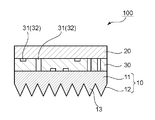
- FIG. 1 is a schematic cross-sectional view illustrating an optical member according to an embodiment of the present invention.
- the optical member 100 has a first member (prism sheet) 10, a second member 20, and an adhesive layer 30.
- the prism sheet 10 typically has a base portion 11 and a prism portion 12.
- the prism unit 12 is configured of a plurality of columnar unit prisms 13 arranged on the opposite side of the base unit 11.
- the adhesive layer 30 has a void 31. By providing the void portion 31, the non-contact portion 32 is defined at the interface between the adhesive layer 30 and the first member 10 and / or the second member 20.
- the void 31 is typically defined by a recess of the surface concavo-convex structure of the adhesive layer 30.
- the void portion 31 may include a through hole penetrating in the thickness direction of the adhesive layer 30, and may be substantially constituted of only the through hole.
- the prism sheet 10 and the second member 20 are integrated.
- the air layer between the prism sheet and the adjacent layer can be eliminated, which can contribute to thinning of the liquid crystal display device. .
- Thinning of the liquid crystal display device has great commercial value because it widens the choice of design.
- by integrating the prism sheet it is possible to avoid the damage of the prism sheet due to the rubbing when attaching the prism sheet to the surface light source device (backlight unit, substantially the light guide plate). Thus, it is possible to prevent the display from becoming hazy, and to obtain a liquid crystal display device excellent in mechanical strength.
- the adhesive layer 30 has the void 31 as described above.
- the void 31 By forming the void, the following advantages can be obtained.
- the conventional optical member in which the prism sheet is integrated and the air layer is eliminated for example, when light from the light source on the back side is incident, the light is not retroreflected and the light is leaked to the viewing side.
- the utilization efficiency of light decreases due to the occurrence of
- a member having a light direction conversion function such as a prism sheet (as another example, a microlens array, a lenticular lens sheet, a diffraction grating, a light guide plate) is integrated, the utilization efficiency of the direction changed light is The above problem is noticeable because it decreases.
- the void portions are not formed at the four corners when the optical member (substantially, the adhesive layer) is viewed in plan as described above.
- the adhesive layer 30 and the first member (a prism sheet in the illustrated example) 10 and the second member 20 are in contact at four corners when the optical member is viewed in plan.
- the first member (in the illustrated example, the prism sheet) 10 and the second member 20 can be closely adhered (integrated) with sufficient strength.
- the utilization efficiency of light can be improved.
- the void portion is not formed in the peripheral portion of the optical member (substantially, the adhesive layer) in plan view.
- the adhesive layer 30 and the first member (in the illustrated example, the prism sheet) 10 and the second member 20 are in contact over the entire peripheral edge of the optical member in plan view.
- any appropriate shape may be adopted as the plan view shape of the gap.
- Specific examples include a circle, an ellipse, an equilateral triangle, an isosceles triangle, an isosceles triangle, a square, a rectangle, a rhombus, a trapezoid, an irregular quadrilateral, a polygon (eg, pentagon, hexagon, heptagon, octagon),
- the shape is star-shaped, bowl-shaped, or indeterminate. You may use combining these shapes.
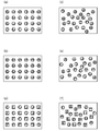
- the void portion may be regularly arranged, for example, as shown in FIG. 2 (a) to FIG. 2 (c) in plan view, for example, as shown in FIG. 2 (d) to FIG. 2 (f). It may be arranged irregularly.
- the arrangement of the voids (in plan view) may be the same or different on both surfaces (the surface on the first member side and the surface on the second member side) of the adhesive layer.
- gap part becomes the same on both surfaces of an adhesive layer.
- the porosity of the adhesive layer in plan view is preferably 70% to 90%, more preferably 73% to 87%, and still more preferably 75% to 85%. If the porosity is in such a range, both the adhesion strength of the first member and the second member and the utilization efficiency of light can be enhanced. Furthermore, a synergistic effect with the formation position of the above-mentioned void may be obtained.
- the porosity when the adhesive layer is viewed in plan means the average of the porosity of both surfaces of the adhesive layer.
- the adhesive layer 30 may be made of any suitable adhesive or pressure-sensitive adhesive as long as it has a predetermined void 31.
- the adhesive layer may preferably be composed of an adhesive. Because the pressure-sensitive adhesive has a suitable thickness, it is easy to form a void that can improve the utilization efficiency of light.
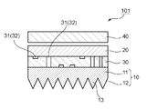
- FIG. 3 is a schematic cross-sectional view illustrating an optical member according to another embodiment of the present invention.
- the illustrated optical member 101 further includes a diffusion plate 40 on the opposite side of the second member 20 to the first member.
- the diffusion plate By providing the diffusion plate, the void portion of the adhesive layer can be made inconspicuous, and an optical member having an excellent appearance can be obtained.
- the diffusion plate 40 is spaced apart from the second member 20. By arranging the diffusion plates apart, it is possible to obtain an optical member having a further excellent appearance.
- the separation distance is, for example, 1 mm or more, preferably 1 mm to 10 mm, and more preferably 2 mm to 5 mm. The separation distance can be adjusted by, for example, a spacer.
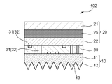
- FIG. 4 is a schematic cross-sectional view illustrating an optical member according to still another embodiment of the present invention.
- the second member 20 is a laminate of two optical films 21 and 22 laminated via another adhesive layer 25.
- another adhesive layer 25 preferably has light diffusibility.
- the void portion of the adhesive layer 30 can be made inconspicuous without using a diffusion plate as shown in FIG. 3, and an optical member having an excellent appearance can be obtained.
- the embodiment of FIG. 4 is an alternative embodiment to the embodiment of FIG.
- another adhesive layer 25 may be composed of a light diffusion adhesive.
- a diffusion plate like FIG. 3 can be used on the opposite side to the 1st member of a 2nd member.
- the prism portion 12 of the prism sheet 10 is disposed on the opposite side to the adhesive layer 30, the prism portion 12 may be disposed on the adhesive layer 30 side. Good.
- first member a prism sheet as a representative example
- adhesive layer a prism sheet as a representative example
- second member constituting the optical member of the present embodiment
- the prism sheet 10 typically has the base portion 11 and the prism portion 12.
- the prism sheet 10 is used for the liquid crystal display device by totally reflecting the light emitted from the back light unit inside the prism unit 12. It is led to the polarizing plate as light having the maximum intensity in the substantially normal direction.
- the base 11 may be omitted depending on the purpose and the configuration of the prism sheet. For example, when the layer adjacent to the base material part side of a prism sheet can function as a support member, the base material part 11 may be omitted.
- the prism sheet 10 (substantially, the prism portion 12) is typically configured by arranging a plurality of columnar unit prisms 13 that are convex on the side opposite to the base portion 11.
- the unit prisms 13 have a columnar shape, and the longitudinal direction (the ridge line direction) is configured to be substantially orthogonal to or substantially parallel to the transmission axis of the polarizing plate in the liquid crystal display device.
- the prism sheet is disposed so that the unit prism is on the opposite side to the adhesive layer, but the unit prism may be disposed on the adhesive layer side.
- the shape of the unit prism 13 may be any suitable configuration as long as the effects of the present invention can be obtained.
- the unit prism 13 may have a triangular cross-sectional shape in a cross section parallel to the arrangement direction and parallel to the thickness direction, and other shapes (for example, one or both slopes of the triangle have different inclination angles) It may be a shape having a plurality of flat surfaces).
- the triangular shape may be a shape (for example, an irregular triangle) which is asymmetric with respect to a straight line passing through the vertex of the unit prism and orthogonal to the sheet surface, and a shape which is symmetrical with respect to the straight line (for example It may be an equilateral triangle).
- the apexes of the unit prisms may be in the form of chamfered curved surfaces, or may be cut so as to have flat ends and have a trapezoidal cross section.
- the detailed shape of the unit prism 13 can be appropriately set according to the purpose.
- the configuration described in JP-A-11-84111 can be adopted as the unit prism 13.
- the heights of the unit prisms 13 may be the same for all unit prisms or may have different heights. If the unitary prisms have different heights, in one embodiment, the unitary prisms have two heights. For example, high and low unit prisms may be alternately arranged, and high (or low) high unit prisms may be arranged every three, four, five, etc. Well, they may be randomly arranged according to the purpose, or may be randomly arranged. In another embodiment, the unit prisms have more than two heights.
- the substrate portion 11 and the prism portion 12 may be integrally formed by extruding a single material, or the like.
- the prism portion may be shaped on the film.
- the thickness of the base portion is preferably 25 ⁇ m to 150 ⁇ m. With such a thickness, the handleability and the strength can be excellent.
- a material which comprises the base material part 11 As a material which comprises the base material part 11, arbitrary appropriate materials can be employ
- (meth) acrylic resins such as cellulose triacetate (TAC) and polymethyl methacrylate (PMMA)
- the film is preferably an unstretched film.
- the same material as the material for forming the prism part when forming the prism part on the base material film is used as the material.
- the material for forming a prism portion for example, epoxy acrylate type or urethane acrylate type reactive resin (for example, ionizing radiation curable resin) may be mentioned.
- a light transmitting thermoplastic resin such as a polyester resin such as PC or PET, an acrylic resin such as PMMA or MS, or an annular polyolefin can be used.
- the substrate portion 11 preferably has substantially optical isotropy.
- substantially optically isotropic means that the retardation value is small enough not to substantially affect the optical characteristics of the liquid crystal display.
- the in-plane retardation Re of the base portion is preferably 20 nm or less, and more preferably 10 nm or less.
- the in-plane retardation Re is an in-plane retardation value measured with light of wavelength 590 nm at 23 ° C.
- nx is the refractive index in the direction in which the refractive index is maximized in the plane of the optical member (that is, in the direction of the slow axis)
- ny is the direction perpendicular to the slow axis in the plane (that is, the phase advance Axial refractive index
- d is the thickness (nm) of the optical member.
- the photoelastic coefficient of the base material portion 11 is preferably ⁇ 10 ⁇ 10 ⁇ 12 m 2 / N to 10 ⁇ 10 ⁇ 12 m 2 / N, more preferably ⁇ 5 ⁇ 10 ⁇ 12 m 2 / N It is -5 ⁇ 10 -12 m 2 / N, more preferably -3 ⁇ 10 -12 m 2 / N to 3 ⁇ 10 -12 m 2 / N.
- Adhesive layer 30 may be comprised of any suitable adhesive or adhesive.
- suitable adhesive or pressure-sensitive adhesive include acrylic resins, polyvinyl alcohol resins, epoxy resins, unsaturated polyesters, urethane resins, urea resins, melamine resins and phenol resins.
- a curing agent may be used in combination, if necessary.
- it is an acrylic resin. It is because it is easy to obtain, and desired properties can be realized by adjusting the kind and blending amount of the copolymerization component. More preferably, it is an adhesive containing an acrylic resin.
- Examples of monomer components (copolymer components) constituting the acrylic resin include methyl (meth) acrylate, ethyl (meth) acrylate, n-propyl (meth) acrylate, isopropyl (meth) acrylate, and 2-methyl-2- Nitropropyl (meth) acrylate, n-butyl (meth) acrylate, isobutyl (meth) acrylate, s-butyl (meth) acrylate, t-butyl (meth) acrylate, n-pentyl (meth) acrylate, t-pentyl (meth) ) Acrylate, 3-Pentyl (meth) acrylate, 2,2-dimethylbutyl (meth) acrylate, n-hexyl (meth) acrylate, cetyl (meth) acrylate, n-octyl (meth) acrylate, 2-ethylhexyl (me
- heterocycle-containing (meth) acrylamide derivatives in which the nitrogen atom of the (meth) acrylamide group forms a heterocycle such as N-acryloyl morpholine, N-acryloyl piperidine, N-methacryloyl piperidine, N-acryloyl pyrrolidine etc. are mentioned. These may be used alone or in combination of two or more. Desired properties can be realized by adjusting the type, number and copolymerization ratio of these monomers.
- the adhesive layer is composed of an adhesive
- its thickness is preferably 0.01 ⁇ m to 2 ⁇ m.
- its thickness is preferably 3 ⁇ m to 200 ⁇ m.
- the void 31 is as described in the above section B-1.
- the void may be formed by any suitable method. Specific examples include mechanical punching (e.g. punching, engraving blade punching, plotter, water jet) or removal of a predetermined part of the adhesive layer (e.g. laser processing or chemical dissolution).
- Mechanical punching may be performed in any suitable manner. For example, it may be performed using a punching device in which a plurality of punching blades are arranged in a predetermined pattern, or may be performed using a device such as an XY plotter to move the punching blades.
- Laser processing may be performed in any suitable manner. Any appropriate laser may be employed as the laser. Specific examples thereof include gas lasers such as CO 2 lasers and excimer lasers; solid lasers such as YAG lasers; semiconductor lasers.
- the irradiation conditions (output conditions, moving speed, number of times) of the laser light are the forming material of the adhesive layer (substantially, adhesive or pressure-sensitive adhesive), the thickness of the adhesive layer, the plan view shape of the void, and planar Any appropriate condition may be adopted depending on the void ratio of
- the second member may be any appropriate optical film or substrate depending on the purpose, and specific examples thereof include an absorptive polarizer, a polarizer protective film, a reflective polarizer, and a retardation.
- a film, a substrate with a conductive layer, a wavelength conversion film, and a combination thereof can be mentioned.
- an absorption polarizer, a polarizer protective film, a reflection polarizer, a wavelength conversion film, and a laminate of a polarizing plate and a reflection polarizer will be described, but other optical films and substrates, It is obvious to those skilled in the art that the present invention is similarly applied to combinations thereof (optical laminates) and similar effects can be obtained.
- the absorptive polarizer any suitable polarizer may be employed.
- the resin film forming the polarizer may be a single layer resin film, or may be a laminate of two or more layers.
- the polarizer composed of a single-layer resin film include hydrophilic polymer films such as polyvinyl alcohol (PVA) -based films, partially formalized PVA-based films, ethylene / vinyl acetate copolymer-based partially saponified films, etc.
- PVA polyvinyl alcohol
- those which have been subjected to a dyeing process and a drawing process with a dichroic substance such as iodine and a dichroic dye and a polyene-based oriented film such as a dewatered product of PVA or a dehydrochlorinated product of polyvinyl chloride.
- a polarizer obtained by dyeing a PVA-based film with iodine and uniaxially stretching it is used because of excellent optical properties.
- the staining with iodine is performed, for example, by immersing a PVA-based film in an aqueous iodine solution.
- the stretching ratio of the uniaxial stretching is preferably 3 to 7 times. Stretching may be carried out after the dyeing process or may be carried out while dyeing. Moreover, it may be dyed after being drawn.
- the PVA-based film is subjected to swelling treatment, crosslinking treatment, washing treatment, drying treatment, and the like. For example, by immersing and washing the PVA-based film in water prior to dyeing, it is possible not only to wash the stains and anti-blocking agent on the surface of the PVA-based film, but also to swell the PVA-based film for uneven dyeing It can be prevented.
- the polarizer obtained by using a laminate a laminate of a resin substrate and a PVA-based resin layer (PVA-based resin film) laminated on the resin substrate, or a resin substrate and the resin
- coated-formed to the base material is mentioned.
- coated and formed by the said resin base material applies a PVA-type resin solution to a resin base material, for example, it is made to dry, and a resin base material Forming a PVA-based resin layer thereon to obtain a laminate of the resin base and the PVA-based resin layer; stretching and dyeing the laminate to make the PVA-based resin layer as a polarizer; obtain.
- stretching typically includes dipping the laminate in a boric acid aqueous solution and stretching.
- stretching may optionally further comprise air-stretching the laminate at a high temperature (eg, 95 ° C. or higher) prior to stretching in an aqueous boric acid solution.
- the resulting laminate of resin substrate / polarizer may be used as it is (that is, the resin substrate may be used as a protective layer of polarizer), and the resin substrate is peeled off from the laminate of resin substrate / polarizer.
- any appropriate protective layer depending on the purpose may be laminated on the peeled surface.
- the details of the method for producing such a polarizer are described, for example, in JP-A-2012-73580. The publication is incorporated herein by reference in its entirety.
- the thickness of the polarizer is preferably 25 ⁇ m or less, more preferably 3 ⁇ m to 22 ⁇ m, still more preferably 3 ⁇ m to 15 ⁇ m, and particularly preferably 3 ⁇ m to 12 ⁇ m.
- the polarizer protective film may be composed of any suitable material.
- the material that is the main component of the film include cellulose-based resins such as triacetyl cellulose (TAC), polyester-based, polyvinyl alcohol-based, polycarbonate-based, polyamide-based, polyimide-based, polyether sulfone-based, and polysulfone-based Transparent resins such as polystyrenes, polynorbornenes, polyolefins, (meth) acrylics and acetates can be mentioned.
- TAC triacetyl cellulose
- TAC triacetyl cellulose
- polyester-based polyvinyl alcohol-based
- polycarbonate-based polyamide-based
- polyimide-based polyimide-based
- polyether sulfone-based polysulfone-based
- Transparent resins such as polystyrenes, polynorbornenes, polyolefins, (meth) acrylics and acetates can be mentioned.
- thermosetting resins such as (meth) acrylic resins, urethane resins, (meth) acrylic urethane resins, epoxy resins, and silicone resins, ultraviolet curable resins, and the like can also be mentioned.
- glassy polymers such as siloxane polymers can also be mentioned.
- a polymer film described in JP-A-2001-343529 (WO 01/37007) can also be used.
- a resin composition containing a thermoplastic resin having a substituted or unsubstituted imide group in a side chain, and a thermoplastic resin having a substituted or unsubstituted phenyl group and a nitrile group in a side chain for example, a resin composition having an alternating copolymer of isobutene and N-methyl maleimide and an acrylonitrile / styrene copolymer can be mentioned.
- the polymer film may be, for example, an extrusion of the resin composition.
- the thickness of the polarizer protective film is preferably 20 ⁇ m to 100 ⁇ m.
- the reflective polarizer has a function of transmitting polarized light in a specific polarization state (polarization direction) and reflecting light in other polarization states.
- the reflective polarizer may be a linear polarization separation type or a circular polarization separation type.
- a linearly polarized light separating reflective polarizer will be described.
- a circularly polarized light separation-type reflective polarizer for example, a laminate of a film on which cholesteric liquid crystal is immobilized and a ⁇ / 4 plate can be mentioned.
- FIG. 5 is a schematic perspective view of an example of a reflective polarizer.
- the reflective polarizer is a multilayer laminate in which layers A having birefringence and layers B substantially free of birefringence are alternately stacked.
- the total number of layers in such a multilayer stack may be 50 to 1000.
- the refractive index nx in the x-axis direction of layer A is larger than the refractive index ny in the y-axis direction
- the refractive index nx in the x-axis direction of layer B and the refractive index ny in the y-axis direction are substantially the same. is there.
- the refractive index difference between the layer A and the layer B is large in the x-axis direction and substantially zero in the y-axis direction.
- the x-axis direction is the reflection axis
- the y-axis direction is the transmission axis.
- the refractive index difference between the A layer and the B layer in the x-axis direction is preferably 0.2 to 0.3.
- the x-axis direction corresponds to the extension direction of the reflective polarizer in the method of manufacturing the reflective polarizer.
- the layer A is preferably made of a material that exhibits birefringence by stretching.
- Representative examples of such materials include naphthalene dicarboxylic acid polyesters (eg, polyethylene naphthalate), polycarbonates and acrylic resins (eg, polymethyl methacrylate). Polyethylene naphthalate is preferred.
- the layer B is preferably made of a material that does not substantially exhibit birefringence even when stretched. Typical examples of such materials include copolyesters of naphthalene dicarboxylic acid and terephthalic acid.
- the reflective polarizer transmits light (for example, p-wave) having a first polarization direction at the interface between the A layer and the B layer, and has a second polarization direction orthogonal to the first polarization direction.
- Reflect light eg, s-wave
- the reflected light is partially transmitted as light having the first polarization direction and partially reflected as light having the second polarization direction at the interface between the A layer and the B layer.
- a large number of such reflections and transmissions can be repeated inside the reflective polarizer to increase the light utilization efficiency.
- the reflective polarizer may include a reflective layer R as the outermost layer opposite to the polarizing plate, as shown in FIG.
- a reflective layer R As the outermost layer opposite to the polarizing plate, as shown in FIG.
- Reflective polarizers can typically be made by combining coextrusion and transverse stretching. Co-extrusion may be performed in any suitable manner. For example, it may be a feed block system or a multi manifold system. For example, the material constituting the A layer and the material constituting the B layer are extruded in a feed block, and then multilayered using a multiplier. Such multi-layering devices are known to those skilled in the art. Next, the obtained long multilayer laminate is representatively stretched in a direction (TD) orthogonal to the transport direction. The material constituting the layer A (for example, polyethylene naphthalate) has its refractive index increased only in the stretching direction by the transverse stretching, and as a result, it exhibits birefringence.
- TD direction orthogonal to the transport direction.
- the material constituting the layer A for example, polyethylene naphthalate
- the material constituting the layer A has its refractive index increased only in the stretching direction by the transverse stretching, and as a result, it
- the material constituting the B layer (for example, a copolyester of naphthalene dicarboxylic acid and terephthalic acid) does not increase the refractive index in any direction even by the transverse stretching.
- a reflective polarizer having a reflection axis in the stretching direction (TD) and a transmission axis in the transport direction (MD) can be obtained (TD corresponds to the x-axis direction in FIG. 5 and MD is the y-axis) Corresponding to the direction).
- the stretching operation may be performed using any suitable device.
- the reflective polarizer for example, those described in JP-A-9-507308 can be used.
- the wavelength conversion film typically comprises a matrix and wavelength conversion material dispersed in the matrix.
- Matrix Any appropriate material can be used as a material constituting the matrix (hereinafter also referred to as a matrix material). Such materials include resins, organic oxides, and inorganic oxides.
- the matrix material preferably has low oxygen permeability and moisture permeability, has high light and chemical stability, has a predetermined refractive index, has excellent transparency, and / or has And have excellent dispersibility to the wavelength conversion material.
- the matrix may be practically composed of a resin film or an adhesive.
- the resin film matrix is a resin film
- any appropriate resin can be used as the resin constituting the resin film.
- the resin may be a thermoplastic resin, may be a thermosetting resin, or may be an active energy ray curable resin.
- the active energy ray-curable resin include electron beam-curable resins, ultraviolet-curable resins, and visible light-curable resins.
- the resin include epoxy, (meth) acrylate (eg, methyl methacrylate, butyl acrylate), norbornene, polyethylene, poly (vinyl butyral), poly (vinyl acetate), polyurea, polyurethane, aminosilicone (AMS), Polyphenylmethylsiloxane, polyphenylalkylsiloxane, polydiphenylsiloxane, polydialkylsiloxane, silsesquioxane, fluorosilicone, vinyl and hydride substituted silicones, styrenic polymers (eg polystyrene, aminopolystyrene (APS), poly ( Acrylonitrile ethylene styrene) (AES)), polymers cross-linked with difunctional monomers (for example, divinylbenzene), polyester-based polymers (for example, polyethylene terephtalate) Rate), cellulosic polymers (e.g., triacety
- thermosetting resin or an ultraviolet curable resin, more preferably a thermosetting resin. It is because it can apply suitably, when manufacturing an optical member of the present invention by roll to roll.
- any appropriate pressure-sensitive adhesive can be used as the pressure-sensitive adhesive.
- the pressure-sensitive adhesive preferably has transparency and optical isotropy.
- Specific examples of the pressure-sensitive adhesive include rubber-based pressure-sensitive adhesives, acrylic pressure-sensitive adhesives, silicone-based pressure-sensitive adhesives, epoxy-based pressure-sensitive adhesives, and cellulose-based pressure-sensitive adhesives.
- it is a rubber-based pressure-sensitive adhesive or an acrylic pressure-sensitive adhesive.
- the wavelength conversion material can control the wavelength conversion characteristics of the wavelength conversion film.
- the wavelength conversion material may be, for example, a quantum dot or a phosphor.
- the content of the wavelength conversion material (total content when using two or more types) in the wavelength conversion film is preferably preferably 100 parts by weight of the matrix material (typically, resin or adhesive solid content).
- the amount is 0.01 to 50 parts by weight, more preferably 0.01 to 30 parts by weight. If the content of the wavelength conversion material is in such a range, a liquid crystal display device excellent in the hue balance of all RGB can be realized.
- Quantum dot The emission center wavelength of the quantum dot can be adjusted by the material and / or composition of the quantum dot, particle size, shape and the like.
- the quantum dots can be composed of any suitable material.
- the quantum dots may preferably be composed of an inorganic material, more preferably an inorganic conductor material or an inorganic semiconductor material.
- the semiconductor material includes, for example, semiconductors of II-VI, III-V, IV-VI, and IV groups.
- Specific examples include Si, Ge, Sn, Se, Te, B, C (including diamond), P, BN, BP, BAs, AlN, AlP, AlAs, AlSb, GaN, GaP, GaAs, GaSb, InN, InP, InAs, InSb, ZnO, ZnS, ZnSe, CdS, CdSe, CdSeZn, CdTe, CdTe, HgS, HgSe, HgTe, BeS, BeSe, BeTe, MgS, MgSe, GeS, GeSe, GeS, SnSe, SnSe, SnTe, PbO, PbS, PbSe, PbTe, CuF, CuCl, CuBr, CuI, Si 3 N 4, Ge 3 N 4, Al 2 O 3, (Al, Ga, In) 2 (S, Se, Te) 3, Al 2 CO is mentioned.
- the quantum dots may include p-type dopants or n-type dopants.
- the quantum dot may have a core-shell structure.
- any suitable functional layer single layer or plural layers may be formed around the shell depending on the purpose, and the surface of the shell may be subjected to surface treatment and / or chemical modification. Good.
- any appropriate shape may be adopted as the shape of the quantum dot depending on the purpose. Specific examples thereof include a spherical shape, a scale shape, a plate shape, an oval spherical shape, and an indeterminate shape.
- the size of the quantum dot may be any suitable size depending on the desired emission wavelength.
- the size of the quantum dot is preferably 1 nm to 10 nm, more preferably 2 nm to 8 nm. If the size of the quantum dot is in such a range, each of green and red exhibits sharp emission, and high color rendering can be realized. For example, green light can emit light with a quantum dot size of about 7 nm, and red light can emit light with a size of about 3 nm.
- the size of the quantum dot is an average particle diameter when the quantum dot is, for example, a spherical shape, and is a dimension along the minimum axis in the shape when the shape is any other shape.
- quantum dots The details of the quantum dots are described, for example, in JP-A-2012-169271, JP-A-2015-102857, JP-A-2015-65158, JP-A-2013-544018, and JP-A-2010-53397. The descriptions of these publications are incorporated herein by reference.
- a quantum dot may use a commercial item.
- Phosphor Any suitable phosphor capable of emitting light of a desired color depending on the purpose can be used as the phosphor. Specific examples include red phosphors and green phosphors.
- red phosphors include complex fluoride phosphors activated with Mn 4 + .
- a complex fluoride phosphor contains at least one coordination center (for example, M described below), is surrounded by fluoride ions acting as a ligand, and, if necessary, a counter ion (for example, A A coordination compound whose charge is compensated by Specific examples thereof include A 2 [MF 5 ]: Mn 4+ , A 3 [MF 6 ]: Mn 4+ , Zn 2 [MF 7 ]: Mn 4+ , A [In 2 F 7 ]: Mn 4+ , A 2 [ M'F 6]: Mn 4+, E [M'F 6]: Mn 4+, A 3 [ZrF 7]: Mn 4+, Ba 0.65 Zr 0.35 F 2.70: Mn 4+ and the like.
- A is Li, Na, K, Rb, Cs, NH 4 or a combination thereof.
- M is Al, Ga, In or a combination thereof.
- M ' is Ge, Si, Sn, Ti, Zr or a combination thereof.
- E is Mg, Ca, Sr, Ba, Zn or a combination thereof.
- a complex fluoride phosphor having a coordination number of 6 at the coordination center is preferred. The details of such a red phosphor are described, for example, in JP-A-2015-84327. The description of the publication is incorporated herein by reference in its entirety.
- green phosphors include compounds containing a solid solution of sialon having a ⁇ -type Si 3 N 4 crystal structure as a main component.
- such treatment is performed to reduce the amount of oxygen contained in the sialon crystal to a specific amount (for example, 0.8% by mass) or less.
- a green phosphor that emits sharp light with a narrow peak width can be obtained.
- the details of such a green phosphor are described in, for example, Japanese Patent Application Laid-Open No. 2013-28814. The description of the publication is incorporated herein by reference in its entirety.
- the wavelength conversion film may be a single layer or may have a laminated structure.
- each layer can include wavelength conversion materials that typically have different emission characteristics.
- the thickness of the wavelength conversion film (the total thickness when having a laminated structure) is preferably 1 ⁇ m to 500 ⁇ m, and more preferably 100 ⁇ m to 400 ⁇ m. If the thickness of the wavelength conversion film is in such a range, the conversion efficiency and the durability can be excellent.
- the thickness of each layer when the wavelength conversion film has a laminated structure is preferably 1 ⁇ m to 300 ⁇ m, and more preferably 10 ⁇ m to 250 ⁇ m.
- the water vapor transmission rate (water vapor transmission rate) in terms of a thickness of 50 ⁇ m of the wavelength conversion film is preferably 100 g / m 2 ⁇ day or less, more preferably 80 g / m 2 ⁇ day or less.
- the water vapor transmission rate can be measured by the measurement method based on JIS K7129 in the atmosphere at 40 ° C. and 90% RH.
- the wavelength conversion film preferably has a barrier function against oxygen and / or water vapor.
- “having a barrier function” means controlling the amount of transmission of oxygen and / or water vapor entering the wavelength conversion film to substantially block the wavelength conversion material therefrom.
- the wavelength conversion film can exhibit a barrier function by providing the wavelength conversion material itself with a three-dimensional structure such as a core-shell type or a tetrapod type. Also, the wavelength conversion film can exhibit a barrier function by appropriately selecting a matrix material.
- the wavelength conversion film may further contain any appropriate additive depending on the purpose.
- the additive include a light diffusion material, a material that imparts anisotropy to light, and a material that polarizes light.
- Specific examples of the light diffusion material include fine particles composed of an acrylic resin, a silicone resin, a styrene resin, or a copolymer resin thereof.
- Specific examples of the material that imparts anisotropy to light and / or the material that polarizes light include elliptical spherical fine particles, core-shell type fine particles, and stacked fine particles that have different birefringence in the major axis and the minor axis.
- the type, the number, the blending amount and the like of the additive may be appropriately set depending on the purpose.
- the wavelength conversion film can be formed, for example, by applying a liquid composition containing a matrix material, a wavelength conversion material, and, if necessary, an additive.
- the matrix material is a resin
- the wavelength conversion film may be coated with a liquid composition containing the matrix material, the wavelength conversion material and, if necessary, additives, a solvent and a polymerization initiator, on any appropriate support. And then drying and / or curing.
- the solvent and the polymerization initiator can be appropriately set depending on the type of matrix material (resin) used.
- any appropriate coating method can be used. Specific examples include curtain coating, dip coating, spin coating, print coating, spray coating, slot coating, roll coating, slide coating, blade coating, gravure coating, and wire bar.
- the curing conditions may be appropriately set depending on the type of matrix material (resin) used, the composition of the composition, and the like.
- a wavelength conversion material used to a matrix material
- the wavelength conversion film may be formed on the barrier layer.
- the wavelength conversion film formed on the support can be transferred to other components of the optical member (for example, a retardation film, a substrate with a conductive layer).
- the second member is an optional optical laminate (for example, a laminate of optional optical films, an optional optical film and an optional substrate).
- the optical films, or the optical film and the substrate may be laminated via another adhesive layer 25 as shown in FIG.
- the further adhesive layer 25 may preferably be composed of a light diffusing adhesive.
- the second member is an optical laminate in which a polarizing plate and a reflective polarizer are laminated via separate adhesive layers.
- the polarizing plate is a laminate having an absorptive polarizer and a polarizer protective film on one side or both sides of the absorptive polarizer.
- the absorptive polarizer, the polarizer protective film, and the reflective polarizer are as described in Section C-1, Section C-2, and Section C-3, respectively.
- the light diffusion adhesive will be briefly described below.
- the light diffusion adhesive includes a pressure sensitive adhesive and light diffusing fine particles dispersed in the pressure sensitive adhesive.
- Any appropriate adhesive can be used as the adhesive. Specific examples thereof include rubber-based pressure-sensitive adhesives, acrylic pressure-sensitive adhesives, silicone-based pressure-sensitive adhesives, epoxy-based pressure-sensitive adhesives, cellulose-based pressure-sensitive adhesives and the like, with preference given to acrylic-based pressure-sensitive adhesives.
- an acrylic pressure-sensitive adhesive By using an acrylic pressure-sensitive adhesive, a light diffusion layer excellent in heat resistance and transparency can be obtained.
- the pressure-sensitive adhesive may be used alone or in combination of two or more.
- any appropriate light diffusing particles can be used. Specific examples thereof include inorganic fine particles and polymer fine particles.
- the light diffusing fine particles are preferably polymer fine particles.
- the material of the polymer fine particles include silicone resin, methacrylic resin (for example, polymethyl methacrylate), polystyrene resin, polyurethane resin, and melamine resin. Since these resins have excellent dispersibility in a pressure-sensitive adhesive and an appropriate refractive index difference from the pressure-sensitive adhesive, a light diffusion layer having excellent diffusion performance can be obtained.
- it is a silicone resin and polymethyl methacrylate.
- the shape of the light diffusing fine particles may be, for example, a spherical shape, a flat shape, or an irregular shape.
- the light diffusing fine particles may be used alone or in combination of two or more.
- the volume average particle diameter of the light diffusing fine particles is preferably 1 ⁇ m to 10 ⁇ m, more preferably 1.5 ⁇ m to 6 ⁇ m. By making volume average particle diameter into the said range, the light-diffusion adhesive which has the outstanding light-diffusion performance can be obtained.
- the volume average particle size can be measured, for example, using an ultracentrifugal automatic particle size distribution measuring apparatus.
- Example 1 (Prism sheet) A commercially available notebook PC (manufactured by SONY Corporation, trade name "VAIO Type S”) was disassembled, and the prism sheet included in the back light side was taken out. The diffusion layer provided on the side opposite to the prism portion was removed with ethyl acetate to obtain a prism sheet of this example.
- the backlight extracted from the above notebook PC was used as a light source.
- Reflective polarizer A 40 type TV (product name: AQUOS, product number: LC40-Z5) manufactured by SHARP was disassembled, and a reflective polarizer was taken out from the back light member. The diffusion layers provided on both sides of this reflective polarizer were removed to obtain a reflective polarizer of this example.
- Adhesive layer with void An acrylic pressure-sensitive adhesive (sheet-like, 23 ⁇ m thick) was prepared. Using a laser processing machine (manufactured by GCC, product name “LaserPro Spirit”, CO 2 laser), through holes of a hexagonal shape in plan view as shown in FIG. . The size in plan view of the hole was 15 mm in maximum diameter, and the porosity in plan view was 85%. The through-hole was not formed in the peripheral part containing the four corners of an adhesive sheet. Thus, the adhesive sheet in which the through-holes were formed was used as the adhesive layer of this example.
- the above reflective polarizer was bonded to a polarizing plate (trade name “SEG1425” manufactured by Nitto Denko Corporation) via an acrylic adhesive.
- the above-mentioned prism sheet was bonded to the reflective polarizer side of the laminate of polarizing plate / reflective polarizer via the above-mentioned adhesive layer.
- the prism sheet was bonded to the laminate so that the prism portion was on the opposite side of the reflection type polarizer, and a laminate having the constitution of polarizing plate / reflection type polarizer / adhesive layer / prism sheet was obtained. .
- the surface of the obtained laminate on the polarizing plate side is bonded to a glass plate (0.7 mm in thickness) via an acrylic pressure-sensitive adhesive, and a laminate having a configuration of glass plate / polarizing plate / adhesive layer / prism sheet is obtained. Obtained.
- the diffusion plate was placed on the glass plate of the obtained laminate to obtain an optical member.
- the obtained optical member was placed on the light source such that the prism sheet was on the light source side, and was subjected to the evaluation of the following (1) and (2). The results are shown in Table 1.
- Example 2 An optical member was obtained in the same manner as in Example 1 except that the diffusion plate was disposed 3 mm apart from the optical member. The obtained optical member was subjected to the same evaluation as in Example 1. The results are shown in Table 1.
- Example 3 An optical member was obtained in the same manner as in Example 1 except that the diffusion plate was not disposed. The obtained optical member was subjected to the same evaluation as in Example 1. The results are shown in Table 1.
- Comparative Example 1 An optical member was obtained in the same manner as in Example 1 except that an acrylic pressure-sensitive adhesive sheet in which no through hole was formed was used as an adhesive layer. The obtained optical member was subjected to the same evaluation as in Example 1. The results are shown in Table 1.
- the optical member of the present invention can be suitably used for a liquid crystal display device.
- the liquid crystal display device using such an optical member is a portable information terminal (PDA), a mobile phone, a clock, a digital camera, a portable device such as a portable game machine, a personal computer monitor, a notebook computer, an OA device such as a copier, video Cameras, LCD TVs, household electrical appliances such as microwave ovens, back monitors, monitors for car navigation systems, automotive devices such as car audio systems, display devices such as information monitors for commercial stores, security devices such as surveillance monitors, It can be used for various applications such as nursing care and medical equipment such as a nursing care monitor and medical monitoring.
Landscapes
- Physics & Mathematics (AREA)
- General Physics & Mathematics (AREA)
- Optics & Photonics (AREA)
- Nonlinear Science (AREA)
- Mathematical Physics (AREA)
- Chemical & Material Sciences (AREA)
- Crystallography & Structural Chemistry (AREA)
- Liquid Crystal (AREA)
- Optical Elements Other Than Lenses (AREA)
- Mounting And Adjusting Of Optical Elements (AREA)
- Glass Compositions (AREA)
Abstract
La présente invention concerne un élément optique qui permet de produire un dispositif d'affichage à cristaux liquides qui est mince et présente une luminance très élevée. Cet élément optique comprend un premier élément ayant une fonction de changement de direction de lumière et un second élément en couches sur le premier élément par le biais d'une couche adhésive. La couche adhésive comporte un espace vide. Une section sans contact est définie au niveau de l'interface entre la couche adhésive et le premier élément et/ou le second élément. La couche adhésive est en contact avec le premier élément et le second élément au niveau de quatre coins lorsqu'elle est observée dans une vue en plan.
Priority Applications (4)
| Application Number | Priority Date | Filing Date | Title |
|---|---|---|---|
| US16/764,738 US11112640B2 (en) | 2017-11-16 | 2018-10-16 | Optical member |
| CN201880074298.7A CN111356944A (zh) | 2017-11-16 | 2018-10-16 | 光学构件 |
| EP18877848.4A EP3712662A4 (fr) | 2017-11-16 | 2018-10-16 | Élément optique |
| KR1020207013877A KR102655465B1 (ko) | 2017-11-16 | 2018-10-16 | 광학 부재 |
Applications Claiming Priority (2)
| Application Number | Priority Date | Filing Date | Title |
|---|---|---|---|
| JP2017221172A JP6993187B2 (ja) | 2017-11-16 | 2017-11-16 | 光学部材 |
| JP2017-221172 | 2017-11-16 |
Publications (1)
| Publication Number | Publication Date |
|---|---|
| WO2019097930A1 true WO2019097930A1 (fr) | 2019-05-23 |
Family
ID=66538942
Family Applications (1)
| Application Number | Title | Priority Date | Filing Date |
|---|---|---|---|
| PCT/JP2018/038411 Ceased WO2019097930A1 (fr) | 2017-11-16 | 2018-10-16 | Élément optique |
Country Status (7)
| Country | Link |
|---|---|
| US (1) | US11112640B2 (fr) |
| EP (1) | EP3712662A4 (fr) |
| JP (1) | JP6993187B2 (fr) |
| KR (1) | KR102655465B1 (fr) |
| CN (1) | CN111356944A (fr) |
| TW (1) | TWI802611B (fr) |
| WO (1) | WO2019097930A1 (fr) |
Families Citing this family (2)
| Publication number | Priority date | Publication date | Assignee | Title |
|---|---|---|---|---|
| JP7686565B2 (ja) * | 2019-09-30 | 2025-06-02 | 日東電工株式会社 | 偏光板のセットおよび該セットを含む画像表示装置 |
| KR102819945B1 (ko) | 2019-10-08 | 2025-06-13 | 주식회사 브이씨 | 홀 위치 업데이트 장치, 홀 위치 업데이트 시스템 및 홀 커터 |
Citations (17)
| Publication number | Priority date | Publication date | Assignee | Title |
|---|---|---|---|---|
| JPS5346066B2 (fr) | 1972-04-14 | 1978-12-11 | ||
| JPH09507308A (ja) | 1993-12-21 | 1997-07-22 | ミネソタ マイニング アンド マニュファクチャリング カンパニー | 光学偏光装置 |
| JPH1184111A (ja) | 1987-11-12 | 1999-03-26 | Mitsubishi Rayon Co Ltd | 面光源素子用プリズムシート |
| WO2001037007A1 (fr) | 1999-11-12 | 2001-05-25 | Kaneka Corporation | Film transparent |
| JP2001343529A (ja) | 2000-03-30 | 2001-12-14 | Kanegafuchi Chem Ind Co Ltd | 偏光子保護フィルムおよびその製造方法 |
| JP2003084137A (ja) * | 2001-07-02 | 2003-03-19 | Sumitomo Chem Co Ltd | 半透過半反射性偏光素子及びそれの光学装置への適用 |
| JP2009025774A (ja) * | 2007-07-24 | 2009-02-05 | Toppan Printing Co Ltd | レンズシート、ディスプレイ用光学シート及びそれを用いたバックライトユニット、ディスプレイ装置 |
| JP2010533976A (ja) | 2007-07-18 | 2010-10-28 | キユーデイー・ビジヨン・インコーポレーテツド | 固体照明に有用な量子ドットベースの光シート |
| JP2012073580A (ja) | 2010-09-03 | 2012-04-12 | Nitto Denko Corp | 薄型偏光膜の製造方法 |
| JP2012169271A (ja) | 2011-02-11 | 2012-09-06 | Lg Innotek Co Ltd | 表示装置 |
| JP2013028814A (ja) | 2005-12-08 | 2013-02-07 | National Institute For Materials Science | 蛍光体とその製造方法 |
| JP2013544018A (ja) | 2010-11-10 | 2013-12-09 | ナノシス・インク. | 量子ドットフィルム、照明装置、および照明方法 |
| JP2015065158A (ja) | 2013-08-26 | 2015-04-09 | 富士フイルム株式会社 | 光変換部材、バックライトユニット、および液晶表示装置、ならびに光変換部材の製造方法 |
| JP2015084327A (ja) | 2006-02-28 | 2015-04-30 | ジーイー ライティング ソリューションズ エルエルシー | 発光ダイオード用途に使用するための赤色線放出蛍光体 |
| JP2015102857A (ja) | 2013-11-28 | 2015-06-04 | 富士フイルム株式会社 | 光変換部材、バックライトユニット、および液晶表示装置、ならびに光変換部材の製造方法 |
| JP2017068250A (ja) | 2015-09-28 | 2017-04-06 | 日東電工株式会社 | 光学部材、ならびに、該光学部材を用いた偏光板のセットおよび液晶表示装置 |
| JP2017090578A (ja) * | 2015-11-05 | 2017-05-25 | サンテックオプト株式会社 | 額縁状の封し部を有する積層光学フィルムシート |
Family Cites Families (13)
| Publication number | Priority date | Publication date | Assignee | Title |
|---|---|---|---|---|
| JPS5628471Y2 (fr) | 1976-09-24 | 1981-07-07 | ||
| JP2003215570A (ja) * | 2002-01-22 | 2003-07-30 | Sumitomo Chem Co Ltd | 半透過半反射型液晶表示装置とそれ用の光源装置及びフィルム |
| TW557371B (en) * | 2001-07-02 | 2003-10-11 | Sumitomo Chemical Co | Semi-transparent-semi-reflectivity film, semi- transparent-semi-reflectivity polarized film, polarized light device using these films, and liquid crystal display device using these films |
| US7010212B2 (en) * | 2002-05-28 | 2006-03-07 | 3M Innovative Properties Company | Multifunctional optical assembly |
| US6846089B2 (en) | 2003-05-16 | 2005-01-25 | 3M Innovative Properties Company | Method for stacking surface structured optical films |
| US7924368B2 (en) * | 2005-12-08 | 2011-04-12 | 3M Innovative Properties Company | Diffuse multilayer optical assembly |
| JP2007294465A (ja) * | 2007-05-17 | 2007-11-08 | Epson Imaging Devices Corp | 照明装置、電気光学装置及び電子機器 |
| JP5104459B2 (ja) | 2008-03-27 | 2012-12-19 | 凸版印刷株式会社 | 光学部材とそれを用いたバックライト・ユニット、ディスプレイ |
| US8870436B2 (en) * | 2008-09-17 | 2014-10-28 | 3M Innovative Properties Company | Patterned adhesives for reflectors |
| JP5529665B2 (ja) * | 2009-11-16 | 2014-06-25 | 住友化学株式会社 | 偏光板、ならびにこれを用いた液晶パネルおよび液晶表示装置 |
| JP5812444B2 (ja) * | 2012-04-13 | 2015-11-11 | 日東電工株式会社 | 光学部材、偏光板のセットおよび液晶表示装置 |
| KR20180036999A (ko) * | 2015-08-05 | 2018-04-10 | 쓰리엠 이노베이티브 프로퍼티즈 컴파니 | 광학 확산 필름 라미네이트 및 제조 방법 |
| KR102679539B1 (ko) * | 2016-12-06 | 2024-06-28 | 삼성디스플레이 주식회사 | 표시 장치 |
-
2017
- 2017-11-16 JP JP2017221172A patent/JP6993187B2/ja active Active
-
2018
- 2018-10-16 WO PCT/JP2018/038411 patent/WO2019097930A1/fr not_active Ceased
- 2018-10-16 KR KR1020207013877A patent/KR102655465B1/ko active Active
- 2018-10-16 EP EP18877848.4A patent/EP3712662A4/fr not_active Withdrawn
- 2018-10-16 CN CN201880074298.7A patent/CN111356944A/zh active Pending
- 2018-10-16 US US16/764,738 patent/US11112640B2/en not_active Expired - Fee Related
- 2018-11-15 TW TW107140509A patent/TWI802611B/zh active
Patent Citations (17)
| Publication number | Priority date | Publication date | Assignee | Title |
|---|---|---|---|---|
| JPS5346066B2 (fr) | 1972-04-14 | 1978-12-11 | ||
| JPH1184111A (ja) | 1987-11-12 | 1999-03-26 | Mitsubishi Rayon Co Ltd | 面光源素子用プリズムシート |
| JPH09507308A (ja) | 1993-12-21 | 1997-07-22 | ミネソタ マイニング アンド マニュファクチャリング カンパニー | 光学偏光装置 |
| WO2001037007A1 (fr) | 1999-11-12 | 2001-05-25 | Kaneka Corporation | Film transparent |
| JP2001343529A (ja) | 2000-03-30 | 2001-12-14 | Kanegafuchi Chem Ind Co Ltd | 偏光子保護フィルムおよびその製造方法 |
| JP2003084137A (ja) * | 2001-07-02 | 2003-03-19 | Sumitomo Chem Co Ltd | 半透過半反射性偏光素子及びそれの光学装置への適用 |
| JP2013028814A (ja) | 2005-12-08 | 2013-02-07 | National Institute For Materials Science | 蛍光体とその製造方法 |
| JP2015084327A (ja) | 2006-02-28 | 2015-04-30 | ジーイー ライティング ソリューションズ エルエルシー | 発光ダイオード用途に使用するための赤色線放出蛍光体 |
| JP2010533976A (ja) | 2007-07-18 | 2010-10-28 | キユーデイー・ビジヨン・インコーポレーテツド | 固体照明に有用な量子ドットベースの光シート |
| JP2009025774A (ja) * | 2007-07-24 | 2009-02-05 | Toppan Printing Co Ltd | レンズシート、ディスプレイ用光学シート及びそれを用いたバックライトユニット、ディスプレイ装置 |
| JP2012073580A (ja) | 2010-09-03 | 2012-04-12 | Nitto Denko Corp | 薄型偏光膜の製造方法 |
| JP2013544018A (ja) | 2010-11-10 | 2013-12-09 | ナノシス・インク. | 量子ドットフィルム、照明装置、および照明方法 |
| JP2012169271A (ja) | 2011-02-11 | 2012-09-06 | Lg Innotek Co Ltd | 表示装置 |
| JP2015065158A (ja) | 2013-08-26 | 2015-04-09 | 富士フイルム株式会社 | 光変換部材、バックライトユニット、および液晶表示装置、ならびに光変換部材の製造方法 |
| JP2015102857A (ja) | 2013-11-28 | 2015-06-04 | 富士フイルム株式会社 | 光変換部材、バックライトユニット、および液晶表示装置、ならびに光変換部材の製造方法 |
| JP2017068250A (ja) | 2015-09-28 | 2017-04-06 | 日東電工株式会社 | 光学部材、ならびに、該光学部材を用いた偏光板のセットおよび液晶表示装置 |
| JP2017090578A (ja) * | 2015-11-05 | 2017-05-25 | サンテックオプト株式会社 | 額縁状の封し部を有する積層光学フィルムシート |
Non-Patent Citations (1)
| Title |
|---|
| See also references of EP3712662A4 |
Also Published As
| Publication number | Publication date |
|---|---|
| US20210181570A1 (en) | 2021-06-17 |
| KR20200087155A (ko) | 2020-07-20 |
| KR102655465B1 (ko) | 2024-04-09 |
| US11112640B2 (en) | 2021-09-07 |
| TWI802611B (zh) | 2023-05-21 |
| EP3712662A4 (fr) | 2021-08-04 |
| JP2019090970A (ja) | 2019-06-13 |
| TW201923436A (zh) | 2019-06-16 |
| JP6993187B2 (ja) | 2022-01-13 |
| EP3712662A1 (fr) | 2020-09-23 |
| CN111356944A (zh) | 2020-06-30 |
Similar Documents
| Publication | Publication Date | Title |
|---|---|---|
| JP6872330B2 (ja) | 光学部材、ならびに、該光学部材を用いた偏光板のセットおよび液晶表示装置 | |
| JP6829969B2 (ja) | 光学部材、ならびに、該光学部材を用いた偏光板のセットおよび液晶表示装置 | |
| CN102265088B (zh) | 用于照明设备和其他照明系统中的光管理的布鲁斯特角膜 | |
| US8619363B1 (en) | Light redirecting element comprising a forward diffracting region and a scattering region | |
| JP6780987B2 (ja) | 光学部材 | |
| JP2012083744A (ja) | 光拡散素子および光拡散素子付偏光板 | |
| KR20180059441A (ko) | 액정 표시 장치 | |
| JP7555394B2 (ja) | 均一な照明のためのバックライト | |
| WO2019097930A1 (fr) | Élément optique | |
| US11125934B2 (en) | Optical member and light guide system | |
| WO2017057395A1 (fr) | Élément optique, et ensemble de plaques polarisantes et dispositif d'affichage à cristaux liquides utilisant cet élément optique | |
| CN109952722A (zh) | 光通信装置及偏光板组件 | |
| WO2018173550A1 (fr) | Filtre optique et dispositif de communication optique |
Legal Events
| Date | Code | Title | Description |
|---|---|---|---|
| 121 | Ep: the epo has been informed by wipo that ep was designated in this application |
Ref document number: 18877848 Country of ref document: EP Kind code of ref document: A1 |
|
| ENP | Entry into the national phase |
Ref document number: 20207013877 Country of ref document: KR Kind code of ref document: A |
|
| NENP | Non-entry into the national phase |
Ref country code: DE |
|
| ENP | Entry into the national phase |
Ref document number: 2018877848 Country of ref document: EP Effective date: 20200616 |