WO2019146920A1 - Procédé de fabrication de dispositif électronique - Google Patents
Procédé de fabrication de dispositif électronique Download PDFInfo
- Publication number
- WO2019146920A1 WO2019146920A1 PCT/KR2018/016744 KR2018016744W WO2019146920A1 WO 2019146920 A1 WO2019146920 A1 WO 2019146920A1 KR 2018016744 W KR2018016744 W KR 2018016744W WO 2019146920 A1 WO2019146920 A1 WO 2019146920A1
- Authority
- WO
- WIPO (PCT)
- Prior art keywords
- thin film
- iodine
- forming
- metal thin
- substrate
- Prior art date
- Legal status (The legal status is an assumption and is not a legal conclusion. Google has not performed a legal analysis and makes no representation as to the accuracy of the status listed.)
- Ceased
Links
Images



Classifications
-
- H—ELECTRICITY
- H10—SEMICONDUCTOR DEVICES; ELECTRIC SOLID-STATE DEVICES NOT OTHERWISE PROVIDED FOR
- H10H—INORGANIC LIGHT-EMITTING SEMICONDUCTOR DEVICES HAVING POTENTIAL BARRIERS
- H10H20/00—Individual inorganic light-emitting semiconductor devices having potential barriers, e.g. light-emitting diodes [LED]
- H10H20/01—Manufacture or treatment
- H10H20/011—Manufacture or treatment of bodies, e.g. forming semiconductor layers
- H10H20/013—Manufacture or treatment of bodies, e.g. forming semiconductor layers having light-emitting regions comprising only Group III-V materials
- H10H20/0137—Manufacture or treatment of bodies, e.g. forming semiconductor layers having light-emitting regions comprising only Group III-V materials the light-emitting regions comprising nitride materials
-
- H—ELECTRICITY
- H10—SEMICONDUCTOR DEVICES; ELECTRIC SOLID-STATE DEVICES NOT OTHERWISE PROVIDED FOR
- H10H—INORGANIC LIGHT-EMITTING SEMICONDUCTOR DEVICES HAVING POTENTIAL BARRIERS
- H10H20/00—Individual inorganic light-emitting semiconductor devices having potential barriers, e.g. light-emitting diodes [LED]
- H10H20/01—Manufacture or treatment
-
- H—ELECTRICITY
- H10—SEMICONDUCTOR DEVICES; ELECTRIC SOLID-STATE DEVICES NOT OTHERWISE PROVIDED FOR
- H10H—INORGANIC LIGHT-EMITTING SEMICONDUCTOR DEVICES HAVING POTENTIAL BARRIERS
- H10H20/00—Individual inorganic light-emitting semiconductor devices having potential barriers, e.g. light-emitting diodes [LED]
- H10H20/01—Manufacture or treatment
- H10H20/011—Manufacture or treatment of bodies, e.g. forming semiconductor layers
- H10H20/012—Manufacture or treatment of bodies, e.g. forming semiconductor layers having light-emitting regions comprising only Group II-IV materials
-
- H—ELECTRICITY
- H10—SEMICONDUCTOR DEVICES; ELECTRIC SOLID-STATE DEVICES NOT OTHERWISE PROVIDED FOR
- H10H—INORGANIC LIGHT-EMITTING SEMICONDUCTOR DEVICES HAVING POTENTIAL BARRIERS
- H10H20/00—Individual inorganic light-emitting semiconductor devices having potential barriers, e.g. light-emitting diodes [LED]
- H10H20/01—Manufacture or treatment
- H10H20/011—Manufacture or treatment of bodies, e.g. forming semiconductor layers
- H10H20/013—Manufacture or treatment of bodies, e.g. forming semiconductor layers having light-emitting regions comprising only Group III-V materials
- H10H20/0133—Manufacture or treatment of bodies, e.g. forming semiconductor layers having light-emitting regions comprising only Group III-V materials with a substrate not being Group III-V materials
- H10H20/01335—Manufacture or treatment of bodies, e.g. forming semiconductor layers having light-emitting regions comprising only Group III-V materials with a substrate not being Group III-V materials the light-emitting regions comprising nitride materials
-
- H—ELECTRICITY
- H10—SEMICONDUCTOR DEVICES; ELECTRIC SOLID-STATE DEVICES NOT OTHERWISE PROVIDED FOR
- H10H—INORGANIC LIGHT-EMITTING SEMICONDUCTOR DEVICES HAVING POTENTIAL BARRIERS
- H10H20/00—Individual inorganic light-emitting semiconductor devices having potential barriers, e.g. light-emitting diodes [LED]
- H10H20/01—Manufacture or treatment
- H10H20/011—Manufacture or treatment of bodies, e.g. forming semiconductor layers
- H10H20/018—Bonding of wafers
-
- H—ELECTRICITY
- H10—SEMICONDUCTOR DEVICES; ELECTRIC SOLID-STATE DEVICES NOT OTHERWISE PROVIDED FOR
- H10H—INORGANIC LIGHT-EMITTING SEMICONDUCTOR DEVICES HAVING POTENTIAL BARRIERS
- H10H20/00—Individual inorganic light-emitting semiconductor devices having potential barriers, e.g. light-emitting diodes [LED]
- H10H20/80—Constructional details
- H10H20/81—Bodies
-
- H—ELECTRICITY
- H10—SEMICONDUCTOR DEVICES; ELECTRIC SOLID-STATE DEVICES NOT OTHERWISE PROVIDED FOR
- H10H—INORGANIC LIGHT-EMITTING SEMICONDUCTOR DEVICES HAVING POTENTIAL BARRIERS
- H10H20/00—Individual inorganic light-emitting semiconductor devices having potential barriers, e.g. light-emitting diodes [LED]
- H10H20/80—Constructional details
- H10H20/81—Bodies
- H10H20/822—Materials of the light-emitting regions
- H10H20/823—Materials of the light-emitting regions comprising only Group II-VI materials, e.g. ZnO
-
- H—ELECTRICITY
- H10—SEMICONDUCTOR DEVICES; ELECTRIC SOLID-STATE DEVICES NOT OTHERWISE PROVIDED FOR
- H10H—INORGANIC LIGHT-EMITTING SEMICONDUCTOR DEVICES HAVING POTENTIAL BARRIERS
- H10H20/00—Individual inorganic light-emitting semiconductor devices having potential barriers, e.g. light-emitting diodes [LED]
- H10H20/80—Constructional details
- H10H20/81—Bodies
- H10H20/822—Materials of the light-emitting regions
- H10H20/824—Materials of the light-emitting regions comprising only Group III-V materials, e.g. GaP
-
- H—ELECTRICITY
- H10—SEMICONDUCTOR DEVICES; ELECTRIC SOLID-STATE DEVICES NOT OTHERWISE PROVIDED FOR
- H10H—INORGANIC LIGHT-EMITTING SEMICONDUCTOR DEVICES HAVING POTENTIAL BARRIERS
- H10H20/00—Individual inorganic light-emitting semiconductor devices having potential barriers, e.g. light-emitting diodes [LED]
- H10H20/80—Constructional details
- H10H20/81—Bodies
- H10H20/822—Materials of the light-emitting regions
- H10H20/824—Materials of the light-emitting regions comprising only Group III-V materials, e.g. GaP
- H10H20/825—Materials of the light-emitting regions comprising only Group III-V materials, e.g. GaP containing nitrogen, e.g. GaN
-
- H—ELECTRICITY
- H10—SEMICONDUCTOR DEVICES; ELECTRIC SOLID-STATE DEVICES NOT OTHERWISE PROVIDED FOR
- H10H—INORGANIC LIGHT-EMITTING SEMICONDUCTOR DEVICES HAVING POTENTIAL BARRIERS
- H10H20/00—Individual inorganic light-emitting semiconductor devices having potential barriers, e.g. light-emitting diodes [LED]
- H10H20/80—Constructional details
- H10H20/83—Electrodes
- H10H20/832—Electrodes characterised by their material
-
- H—ELECTRICITY
- H10—SEMICONDUCTOR DEVICES; ELECTRIC SOLID-STATE DEVICES NOT OTHERWISE PROVIDED FOR
- H10H—INORGANIC LIGHT-EMITTING SEMICONDUCTOR DEVICES HAVING POTENTIAL BARRIERS
- H10H20/00—Individual inorganic light-emitting semiconductor devices having potential barriers, e.g. light-emitting diodes [LED]
- H10H20/01—Manufacture or treatment
- H10H20/032—Manufacture or treatment of electrodes
Definitions
- the present invention relates to a method of manufacturing an electronic device, and more particularly, to a method of manufacturing an electronic device constituting a PN junction.
- Si semiconductors which have been developed and commercialized since the 1950s, have advantages such as low cost of materials, easy Si oxide obtained by thermal oxidation, and stable surface protective films. It meets the characteristics required by all devices.
- the problem is that it is difficult to grow a large single crystal, and since the band gap is as low as 1.1 eV, it is not suitable as a semiconductor device requiring high thermal stability and high efficiency.
- WBG wide band gap
- III-V compound semiconductors and II-VI compound semiconductors have wide bandgap semiconductors, which are valuable as high-power, high-frequency electronic devices.
- Mg doping is generally required to form a p-type semiconductor, and the Mg-doped III-V compound semiconductors or II-VI compound semiconductors are poor in the performance of p-type semiconductors due to hydrogen bonding.
- strong chemical bonding forces serve as disadvantages, making crystal growth and device processing difficult. Due to these phenomena, wide bandgap semiconductors are limited in application to various fields.
- a method of manufacturing an electronic device includes the steps of preparing a substrate, forming an n-type semiconductor including a III-V compound semiconductor or a II-VI compound semiconductor material on the substrate, And forming a metal thin film including at least one of copper (Cu), silver (Ag), gold (Au), titanium (Ti), and nickel (Ni) on the n-type semiconductor, And forming a p-type semiconductor on the n-type semiconductor by iodinating the metal thin film using any one of liquid iodine (I), solid iodine (I) and gaseous iodine (I).
- the step of iodinating the metal thin film includes a step of immersing the substrate on which the metal thin film is formed in liquid iodine, a step of taking out the substrate on which the metal thin film is formed from the liquid iodine, and a step of removing residual iodine can do.
- the step of immersing the substrate on which the metal thin film is formed in liquid iodine may be performed within a range of 60 to 100 seconds.
- the step of immersing or removing the substrate on which the metal thin film is formed in liquid iodine may be performed while the substrate is turned upside down so that the metal thin film faces downward.
- the step of removing residual iodine may be performed by heating the substrate or blowing nitrogen (N 2) to the substrate, in which case the substrate may be carried out in an inverted state.
- the step of iodinating the metal thin film may be performed by contacting solid metal iodine with the metal thin film in an air or nitrogen atmosphere at room temperature.
- the contact time of the solid iodine with the metal thin film is 12 hours or more.
- the step of iodinating the metal thin film may be performed by heating and vaporizing the solid iodine, and blowing the vaporized iodine to the metal thin film.
- the step of iodinating the metal thin film may further include heating the solid iodine to vaporize, and then mixing the vaporized iodine with the carrier gas.
- the carrier gas is nitrogen (N 2) gas
- the step of blowing vaporized iodine into the metal thin film may be performed for 10 minutes to 60 minutes.
- the group II-VI compound semiconductors may be any one or a combination of two or more members selected from the group consisting of GaN, GaP, GaAs, InP, AlGaN, AlGaP, AlInGaN, InGaAs, , CdSe, CdTe, ZnO, ZnS, ZnSe, ZnTe, CdZnTe, HgCdTe, HgZnTe, or a combination of two or more thereof.
- the method of manufacturing an electronic device may further include forming a first cladding layer including a III-V semiconductor or a II-VI semiconductor material on the n-type semiconductor after forming the n-type semiconductor, Forming an active layer including a III-V semiconductor or a II-VI semiconductor material on the first cladding layer, and forming a second cladding layer including an I-VII semiconductor on the active layer Step < / RTI >
- the method of manufacturing an electronic device since a semiconductor is grown naturally without forming a doping process when forming a p-type semiconductor, it can be advantageous for forming a high-purity single crystal. In addition, defects due to lattice mismatch with the substrate can be solved at the source.
- group I-VII compound semiconductors can grow crystals at a low temperature, so that the process is easy and the material stability can be secured.
- FIG. 1 is a cross-sectional view of a light emitting device according to an exemplary embodiment of the present invention.
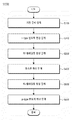
- FIG. 2 is a flowchart of a method of manufacturing a light emitting device according to an exemplary embodiment of the present invention.
- FIG. 3 and FIG. 4 are photographs depicting changes in copper iodide immersed in copper thin film and liquid iodine as a result of experiments of the present invention.
- FIG. 5 is a SEM photograph of the copper iodide thin film of FIG.
- first, second, etc. may be used to describe various components, but the components should not be limited by the terms. The terms are used only for the purpose of distinguishing one component from another.
- first component may be referred to as a second component, and similarly, the second component may also be referred to as a first component.
- FIG. 1 is a cross-sectional view of an electronic device 1000 according to the present invention.
- an electronic device 1000 includes a substrate 100, a first semiconductor layer 200, and a second semiconductor layer 700.
- the electronic device 1000 may further include at least one of a first cladding layer 300, an active layer 400, and a second cladding layer 600.
- the first semiconductor layer 200 is formed on the substrate 100 and may include a III-V compound semiconductor or a II-VI compound semiconductor.
- the first cladding layer 300 may be formed on the first semiconductor layer 200.
- the active layer 400 may be formed on the first cladding layer 300 and may include a III-V compound semiconductor or a II-VI compound semiconductor.
- the second cladding layer 600 may be formed on the active layer 400.
- the second semiconductor layer 700 may be formed of an I-VII compound semiconductor on the second cladding layer 600.
- the first semiconductor layer 200 may be an n-type semiconductor
- the second semiconductor layer 700 may be a p-type semiconductor.
- III-V compound semiconductors or II-VI compound semiconductors are mainly used to form wide band gap semiconductors.
- Impurity doping treatment is inevitable.
- the Group III-V compound semiconductor and the Group II-VI compound semiconductor are doped with Mg to form a p-type semiconductor, the hole generating ability is deteriorated due to strong hydrogen bonding, and the efficiency is reduced.
- the p-type semiconductor is formed only by the crystal growth of the group I-VII compound semiconductors, the process is easy and the process can be performed at a low temperature.
- the group I-VII compound semiconductors have a higher band gap energy than the group III-V compound semiconductors and the group II-VI compound semiconductors.
- the first cladding layer 300 may be formed of a III-V compound semiconductor or a II-VI compound semiconductor.
- the second cladding layer 600 may be made of a Group I-VII compound semiconductor.
- the first cladding layer 300 and the second cladding layer 600 may be formed according to the present invention to overcome the limit of optical efficiency.
- the electronic device 1000 may further include a third cladding layer 500 between the active layer 400 and the second cladding layer 600 and the third cladding layer 500 may include a III- V compound semiconductor or a II-VI compound semiconductor material.
- I -VII compound semiconductors have a Wurtzite crystal structure, whereas copper (Cu) -based I-VII group compound semiconductors have a zinc blend crystal structure, Due to the structure, high quality crystal growth is not easy.
- the electronic device 1000 may be a buffer for hetero-epitaxial growth by forming a third cladding layer 500 including a III-V compound semiconductor or a II-VI compound semiconductor material . Defects due to lattice mismatch can be originally solved by growing a Group I-VII compound semiconductor on the third cladding layer 500.
- a transparent electrode layer 800 may be further formed on the second semiconductor layer.
- the transparent electrode layer 800 may be made of any one of Ni / Au, ITO, CTO, TiWN, IN 2 O 3 , SnO 2 , CdO, ZnO, CuGaO 2 and SrCu 2 O 2 .
- the electronic device 1000 according to the present invention may further include a phosphor layer (not shown), which is applicable to products in various types of lighting and displays.
- the electronic device may include a light conversion layer including a semiconductor element and a phosphor.
- the electronic device may include a substrate, an n-type semiconductor layer, a first cladding layer, an active layer, a second cladding layer, and a p-type semiconductor layer.
- the n-type semiconductor layer may be formed of a III-V compound semiconductor or a II-VI compound semiconductor on the substrate.
- the first cladding layer may be formed of a III-V compound semiconductor or a II-VI compound semiconductor on the n-type semiconductor layer.
- the active layer may be formed of a III-V compound semiconductor or a II-VI compound semiconductor on the first cladding layer.
- the second cladding layer may be formed of an I-VII compound semiconductor on the active layer.
- the p-type semiconductor layer may be formed of an I-VII compound semiconductor on the second cladding layer.
- the light emitting diode may further include a third cladding layer between the active layer and the second cladding layer, and the third cladding layer may be formed of a III-V compound semiconductor or a II-VI compound semiconductor.
- FIG. 2 is a flowchart of a method of manufacturing a light emitting device according to an exemplary embodiment of the present invention.
- a method of manufacturing an electronic device (S1000) according to the present invention includes a step of preparing a substrate (S100), a step of forming an n-type semiconductor (S200) and a step of forming a p- ). Meanwhile, the method for fabricating an electronic device (S1000) according to the present invention may include any one of forming a first cladding layer (S300), forming an active layer (S400), and forming a second cladding layer (S500) .
- the step of forming the n-type semiconductor (S200) may use an n-type semiconductor including a III-V compound semiconductor or a II-VI compound semiconductor material, and may be formed on the substrate.
- the forming of the first cladding layer (S300) may be performed on the n-type semiconductor.
- the step of forming the active layer (S400) may be formed on the first cladding layer, and the active layer may include a III-V compound semiconductor or a II-VI compound semiconductor material.
- the forming of the second cladding layer (S500) may be performed on the active layer.
- the step of forming the p-type semiconductor (S600) may be formed on the second cladding layer, and the step of forming the metal thin film and the step of iodinating the metal thin film may be performed.
- the metal thin film may include at least one of copper (Cu), silver (Ag), gold (Au), titanium (Ti), and nickel (Ni).
- the metal thin film may be formed, for example, by a vapor deposition method or a sputtering method.
- the thickness of the metal thin film is preferably 1 nm or less.
- the step of iodinating the metal thin film may use liquid iodine (I), solid iodine (I), and gaseous iodine (I).
- a method using liquid iodine is described. First, a substrate on which a metal thin film is formed is immersed in liquid iodine. As a result of the experiment, when the liquid iodine having a purity of 99% was used, it was confirmed that the copper thin film with a thickness of 1 nm completely changed into copper iodide (CuI) after about 60 seconds to 100 seconds elapsed.
- CuI copper iodide
- the substrate on which the metal thin film is formed is taken out from the liquid iodine.
- the substrate is taken out with the metal thin film facing downward. In this manner, when the substrate is taken out in an inverted state, the liquid iodine remaining on the substrate is evenly distributed in each region of the substrate, and uniformity of the electronic device formed in each region of the substrate can be achieved.
- the substrate may be heated, blown, or blown with heating.
- the heating temperature of the substrate can be heated to about 100 ⁇ , and nitrogen (N 2 ) gas can be blown.
- the resistivity was found to be 0.1 to 0.5 ⁇ ⁇ cm, the bulk carrier density to 1 ⁇ 10 18 to 5 ⁇ 10 18 cm -3 and the mobility to 10 to 30 cm 2 V -1 S -1 Respectively.
- a method using solid iodine is explained.
- solid iodine is brought into contact with the metal thin film.
- the contact time is more than 12 hours in order to change the copper film of 1 nm thickness into copper iodide.
- the resistance is 0.01 to 0.05 ⁇ ⁇ cm
- the bulk carrier density is 1 ⁇ 10 19 to 5 ⁇ 10 19 cm -3
- the mobility is 1 to 10 cm 2 V -1 S -1 .
- the bulk carrier density is increased to 10 as compared with the case of applying iodine in the liquid state, and the resistance is greatly reduced to about 1/10, and the mobility is also greatly reduced.
- iodine gas As another embodiment, a method of using iodine gas as a step of iodizing the metal thin film will be described. First, solid iodine is heated to vaporize, and then vaporized iodine is blown into the metal thin film. For example, solid iodine can be heated to about 80 ° C.
- vaporized iodine may be mixed with the carrier gas, and then the mixed gas may be blown into the metal thin film.
- nitrogen gas or argon gas can be used as the carrier gas.
- the resistance is 0.01 to 0.05 ⁇ ⁇ cm
- the bulk carrier density is 1 ⁇ 10 19 to 5 ⁇ 10 19 cm -3 , 1 to 10 cm 2 V -1 S -1 .
- liquid iodine and solid or gaseous iodine can be used.
- the method for fabricating an electronic device further includes forming a third cladding layer between the forming of the active layer (S400) and the forming of the second cladding layer (S500) .
- the third cladding layer may include a III-V compound semiconductor or a II-VI compound semiconductor material.
- the method for fabricating a semiconductor light emitting device may be performed sequentially or two or more steps at the same time, but the order is not limited.
- the Group III-V compound semiconductor may be formed of any one or a combination of two or more of GaN, GaP, GaAs, InP, AlGaN, AlGaP, AlInGaN, InGaAs, and GaAsP.
- the Group II-VI compound semiconductor may be formed of any one or a combination of two or more of CdO, CdS, CdSe, CdTe, ZnO, ZnS, ZnSe, ZnTe, CdZnTe, HgCdTe and HgZnTe.
- the method of manufacturing an electronic device since a semiconductor is grown naturally without forming a doping process when forming a p-type semiconductor, it can be advantageous for forming a high-purity single crystal. In addition, defects due to lattice mismatch with the substrate can be solved at the source.
- group I-VII compound semiconductors can grow crystals at a low temperature, so that the process is easy and the material stability can be secured.
Landscapes
- Led Devices (AREA)
Abstract
L'invention concerne un procédé de fabrication d'un dispositif électronique comprenant les étapes consistant à : préparer un substrat; former un semi-conducteur de type n comprenant un semi-conducteur composé du groupe III-V ou un matériau semi-conducteur composé du groupe II-VI sur le substrat; former une couche mince métallique comprenant au moins un élément parmi le cuivre (Cu), l'argent (Ag), l'or (Au), le titane (Ti) et le nickel (Ni) sur la partie supérieure du semi-conducteur de type n; et former un semi-conducteur de type p sur la partie supérieure du semi-conducteur de type n en réalisant une iodation d'une couche mince métallique à l'aide d'un élément quelconque parmi l'iode liquide (I), l'iode solide (I), ou l'iode gazeux (I). Par conséquent, il est possible de surmonter la limite de l'efficacité lumineuse du semi-conducteur de type p en fournissant un dispositif électronique de type hybride et son procédé de fabrication.
Priority Applications (1)
| Application Number | Priority Date | Filing Date | Title |
|---|---|---|---|
| US16/965,473 US11355663B2 (en) | 2018-01-29 | 2018-12-27 | Method of manufacturing an electronic device |
Applications Claiming Priority (2)
| Application Number | Priority Date | Filing Date | Title |
|---|---|---|---|
| KR10-2018-0010627 | 2018-01-29 | ||
| KR1020180010627A KR101948072B1 (ko) | 2018-01-29 | 2018-01-29 | 전자소자 제조방법 |
Publications (1)
| Publication Number | Publication Date |
|---|---|
| WO2019146920A1 true WO2019146920A1 (fr) | 2019-08-01 |
Family
ID=65366109
Family Applications (1)
| Application Number | Title | Priority Date | Filing Date |
|---|---|---|---|
| PCT/KR2018/016744 Ceased WO2019146920A1 (fr) | 2018-01-29 | 2018-12-27 | Procédé de fabrication de dispositif électronique |
Country Status (3)
| Country | Link |
|---|---|
| US (1) | US11355663B2 (fr) |
| KR (1) | KR101948072B1 (fr) |
| WO (1) | WO2019146920A1 (fr) |
Families Citing this family (3)
| Publication number | Priority date | Publication date | Assignee | Title |
|---|---|---|---|---|
| KR101498656B1 (ko) * | 2013-10-08 | 2015-03-05 | 서울시립대학교 산학협력단 | 투명화 장치 및 그 방법 |
| KR102424796B1 (ko) * | 2020-09-18 | 2022-07-26 | 성균관대학교산학협력단 | 칼코겐 원소로 도핑된 요오드화 구리 박막 및 이의 제조 방법 |
| KR102800365B1 (ko) * | 2023-11-28 | 2025-04-23 | 인천대학교 산학협력단 | 결함 상태 제어를 통한 구리-요오드 박막의 제조방법 |
Citations (5)
| Publication number | Priority date | Publication date | Assignee | Title |
|---|---|---|---|---|
| WO2009106583A1 (fr) * | 2008-02-29 | 2009-09-03 | Dublin City University | Dispositif électroluminescent |
| KR20120057646A (ko) * | 2009-11-18 | 2012-06-05 | 서울시립대학교 산학협력단 | 구리 블렌드 ⅰ- ⅶ 화합물 반도체 발광 디바이스 |
| KR20140003124A (ko) * | 2012-06-29 | 2014-01-09 | 인텔렉추얼디스커버리 주식회사 | 반도체 발광 디바이스 |
| KR101548901B1 (ko) * | 2015-02-09 | 2015-09-01 | 성균관대학교산학협력단 | 이종접합 소자의 제조 방법 및 이종접합 소자 |
| KR20170140563A (ko) * | 2016-06-13 | 2017-12-21 | 주식회사 페타룩스 | 반도체 발광장치 및 제조방법 |
Family Cites Families (5)
| Publication number | Priority date | Publication date | Assignee | Title |
|---|---|---|---|---|
| KR100404942B1 (ko) * | 2000-06-20 | 2003-11-07 | 주식회사 하이닉스반도체 | 반도체 소자의 금속 배선 형성 방법 |
| WO2010038740A1 (fr) * | 2008-10-03 | 2010-04-08 | 昭和電工株式会社 | Procédé de fabrication d’un élément luminescent semi-conducteur |
| WO2012121067A1 (fr) * | 2011-03-08 | 2012-09-13 | 独立行政法人科学技術振興機構 | Procédé de fabrication de structure d'électrode ayant une longueur d'espace nanoscopique, structure d'électrode ayant une longueur d'espace nanoscopique ainsi obtenue, et nanodispositif |
| US8524581B2 (en) * | 2011-12-29 | 2013-09-03 | Intermolecular, Inc. | GaN epitaxy with migration enhancement and surface energy modification |
| US9263327B2 (en) * | 2014-06-20 | 2016-02-16 | Globalfoundries Inc. | Minimizing void formation in semiconductor vias and trenches |
-
2018
- 2018-01-29 KR KR1020180010627A patent/KR101948072B1/ko active Active
- 2018-12-27 WO PCT/KR2018/016744 patent/WO2019146920A1/fr not_active Ceased
- 2018-12-27 US US16/965,473 patent/US11355663B2/en active Active
Patent Citations (5)
| Publication number | Priority date | Publication date | Assignee | Title |
|---|---|---|---|---|
| WO2009106583A1 (fr) * | 2008-02-29 | 2009-09-03 | Dublin City University | Dispositif électroluminescent |
| KR20120057646A (ko) * | 2009-11-18 | 2012-06-05 | 서울시립대학교 산학협력단 | 구리 블렌드 ⅰ- ⅶ 화합물 반도체 발광 디바이스 |
| KR20140003124A (ko) * | 2012-06-29 | 2014-01-09 | 인텔렉추얼디스커버리 주식회사 | 반도체 발광 디바이스 |
| KR101548901B1 (ko) * | 2015-02-09 | 2015-09-01 | 성균관대학교산학협력단 | 이종접합 소자의 제조 방법 및 이종접합 소자 |
| KR20170140563A (ko) * | 2016-06-13 | 2017-12-21 | 주식회사 페타룩스 | 반도체 발광장치 및 제조방법 |
Also Published As
| Publication number | Publication date |
|---|---|
| US20210057604A1 (en) | 2021-02-25 |
| KR101948072B1 (ko) | 2019-02-14 |
| US11355663B2 (en) | 2022-06-07 |
Similar Documents
| Publication | Publication Date | Title |
|---|---|---|
| Su et al. | GaN metal-semiconductor-metal ultraviolet sensors with various contact electrodes | |
| WO2016105146A1 (fr) | Diode électroluminescente et matrice de diodes électroluminescentes la comprenant | |
| WO2019146920A1 (fr) | Procédé de fabrication de dispositif électronique | |
| WO2010101332A1 (fr) | Dispositif électroluminescent | |
| WO2011129548A2 (fr) | Ensemble substrat pour la croissance de cristaux et procédé de fabrication d'un dispositif émetteur de lumière utilisant ledit ensemble | |
| WO2010143778A1 (fr) | Substrat semiconducteur, procédé pour le façonner, dispositif à semiconducteur et procédé pour le façonner | |
| WO2014109454A1 (fr) | Diode électroluminescente et procédé de fabrication de celle-ci | |
| US20240363804A1 (en) | Semiconductor stack, semiconductor device and method for manufacturing the same | |
| WO2010055987A1 (fr) | Procédé de fabrication de substrat d'oxyde de gallium, dispositif électroluminescent et son procédé de fabrication | |
| Katoda et al. | Heteroepitaxial growth of gallium phosphide on silicon | |
| WO2010098606A2 (fr) | Procédé de fabrication de dispositif électroluminescent | |
| TWI244222B (en) | A ternary nitride buffer layer containing nitride light-emitting device and manufacturing method of the same | |
| US20220005970A1 (en) | Semiconductor light emitting device and manufacturing method | |
| WO2013066088A1 (fr) | Film mince transparent, dispositif électroluminescent le comprenant, et son procédé de fabrication | |
| WO2011034273A1 (fr) | Dispositif électroluminescent à semi-conducteurs | |
| CN116469954A (zh) | 一种可见光探测器及其制备方法 | |
| JP4799769B2 (ja) | GaP系発光ダイオード | |
| CN216902949U (zh) | 钙钛矿太阳能电池和氮化镓基led集成结构及半导体器件 | |
| WO2017188578A1 (fr) | Électrode transparente pour dispositif électroluminescent ultraviolet et procédé de fabrication associé | |
| WO2020022684A1 (fr) | Diode électroluminescente ayant une couche d'oxyde de zinc et son procédé de fabrication | |
| WO2020218798A1 (fr) | Dispositif électroluminescent à semi-conducteur | |
| TWI856632B (zh) | 半導體疊層、半導體元件及其製造方法 | |
| CN105742160A (zh) | GaN外延片的制作方法及制备GaN外延片的设备 | |
| KR950001620B1 (ko) | 규소저매늄/저매늄 완충층을 이용한 규소기판상의 갈륨비소 박막성장방법 | |
| JPH11322500A (ja) | p型半導体、p型半導体の製造方法、半導体装置 |
Legal Events
| Date | Code | Title | Description |
|---|---|---|---|
| 121 | Ep: the epo has been informed by wipo that ep was designated in this application |
Ref document number: 18902533 Country of ref document: EP Kind code of ref document: A1 |
|
| NENP | Non-entry into the national phase |
Ref country code: DE |
|
| 122 | Ep: pct application non-entry in european phase |
Ref document number: 18902533 Country of ref document: EP Kind code of ref document: A1 |