WO2020021742A1 - Carte de circuit imprimé - Google Patents
Carte de circuit imprimé Download PDFInfo
- Publication number
- WO2020021742A1 WO2020021742A1 PCT/JP2019/005089 JP2019005089W WO2020021742A1 WO 2020021742 A1 WO2020021742 A1 WO 2020021742A1 JP 2019005089 W JP2019005089 W JP 2019005089W WO 2020021742 A1 WO2020021742 A1 WO 2020021742A1
- Authority
- WO
- WIPO (PCT)
- Prior art keywords
- electrode
- electrodes
- solder
- insulating substrate
- printed circuit
- Prior art date
- Legal status (The legal status is an assumption and is not a legal conclusion. Google has not performed a legal analysis and makes no representation as to the accuracy of the status listed.)
- Ceased
Links
Images


Classifications
-
- H—ELECTRICITY
- H05—ELECTRIC TECHNIQUES NOT OTHERWISE PROVIDED FOR
- H05K—PRINTED CIRCUITS; CASINGS OR CONSTRUCTIONAL DETAILS OF ELECTRIC APPARATUS; MANUFACTURE OF ASSEMBLAGES OF ELECTRICAL COMPONENTS
- H05K1/00—Printed circuits
- H05K1/02—Details
- H05K1/14—Structural association of two or more printed circuits
- H05K1/141—One or more single auxiliary printed circuits mounted on a main printed circuit, e.g. modules, adapters
-
- H—ELECTRICITY
- H05—ELECTRIC TECHNIQUES NOT OTHERWISE PROVIDED FOR
- H05K—PRINTED CIRCUITS; CASINGS OR CONSTRUCTIONAL DETAILS OF ELECTRIC APPARATUS; MANUFACTURE OF ASSEMBLAGES OF ELECTRICAL COMPONENTS
- H05K1/00—Printed circuits
- H05K1/02—Details
- H05K1/11—Printed elements for providing electric connections to or between printed circuits
-
- H—ELECTRICITY
- H05—ELECTRIC TECHNIQUES NOT OTHERWISE PROVIDED FOR
- H05K—PRINTED CIRCUITS; CASINGS OR CONSTRUCTIONAL DETAILS OF ELECTRIC APPARATUS; MANUFACTURE OF ASSEMBLAGES OF ELECTRICAL COMPONENTS
- H05K3/00—Apparatus or processes for manufacturing printed circuits
- H05K3/22—Secondary treatment of printed circuits
- H05K3/28—Applying non-metallic protective coatings
-
- H—ELECTRICITY
- H05—ELECTRIC TECHNIQUES NOT OTHERWISE PROVIDED FOR
- H05K—PRINTED CIRCUITS; CASINGS OR CONSTRUCTIONAL DETAILS OF ELECTRIC APPARATUS; MANUFACTURE OF ASSEMBLAGES OF ELECTRICAL COMPONENTS
- H05K3/00—Apparatus or processes for manufacturing printed circuits
- H05K3/30—Assembling printed circuits with electric components, e.g. with resistors
- H05K3/32—Assembling printed circuits with electric components, e.g. with resistors electrically connecting electric components or wires to printed circuits
- H05K3/34—Assembling printed circuits with electric components, e.g. with resistors electrically connecting electric components or wires to printed circuits by soldering
-
- H—ELECTRICITY
- H05—ELECTRIC TECHNIQUES NOT OTHERWISE PROVIDED FOR
- H05K—PRINTED CIRCUITS; CASINGS OR CONSTRUCTIONAL DETAILS OF ELECTRIC APPARATUS; MANUFACTURE OF ASSEMBLAGES OF ELECTRICAL COMPONENTS
- H05K3/00—Apparatus or processes for manufacturing printed circuits
- H05K3/36—Assembling printed circuits with other printed circuits
- H05K3/366—Assembling printed circuits with other printed circuits substantially perpendicularly to each other
-
- H—ELECTRICITY
- H05—ELECTRIC TECHNIQUES NOT OTHERWISE PROVIDED FOR
- H05K—PRINTED CIRCUITS; CASINGS OR CONSTRUCTIONAL DETAILS OF ELECTRIC APPARATUS; MANUFACTURE OF ASSEMBLAGES OF ELECTRICAL COMPONENTS
- H05K1/00—Printed circuits
- H05K1/02—Details
- H05K1/11—Printed elements for providing electric connections to or between printed circuits
- H05K1/117—Pads along the edge of rigid circuit boards, e.g. for pluggable connectors
-
- H—ELECTRICITY
- H05—ELECTRIC TECHNIQUES NOT OTHERWISE PROVIDED FOR
- H05K—PRINTED CIRCUITS; CASINGS OR CONSTRUCTIONAL DETAILS OF ELECTRIC APPARATUS; MANUFACTURE OF ASSEMBLAGES OF ELECTRICAL COMPONENTS
- H05K2201/00—Indexing scheme relating to printed circuits covered by H05K1/00
- H05K2201/03—Conductive materials
- H05K2201/0332—Structure of the conductor
- H05K2201/0335—Layered conductors or foils
- H05K2201/0338—Layered conductor, e.g. layered metal substrate, layered finish layer or layered thin film adhesion layer
-
- H—ELECTRICITY
- H05—ELECTRIC TECHNIQUES NOT OTHERWISE PROVIDED FOR
- H05K—PRINTED CIRCUITS; CASINGS OR CONSTRUCTIONAL DETAILS OF ELECTRIC APPARATUS; MANUFACTURE OF ASSEMBLAGES OF ELECTRICAL COMPONENTS
- H05K2201/00—Indexing scheme relating to printed circuits covered by H05K1/00
- H05K2201/03—Conductive materials
- H05K2201/0332—Structure of the conductor
- H05K2201/0364—Conductor shape
- H05K2201/0367—Metallic bump or raised conductor not used as solder bump
-
- H—ELECTRICITY
- H05—ELECTRIC TECHNIQUES NOT OTHERWISE PROVIDED FOR
- H05K—PRINTED CIRCUITS; CASINGS OR CONSTRUCTIONAL DETAILS OF ELECTRIC APPARATUS; MANUFACTURE OF ASSEMBLAGES OF ELECTRICAL COMPONENTS
- H05K2201/00—Indexing scheme relating to printed circuits covered by H05K1/00
- H05K2201/04—Assemblies of printed circuits
- H05K2201/048—Second PCB mounted on first PCB by inserting in window or holes of the first PCB
-
- H—ELECTRICITY
- H05—ELECTRIC TECHNIQUES NOT OTHERWISE PROVIDED FOR
- H05K—PRINTED CIRCUITS; CASINGS OR CONSTRUCTIONAL DETAILS OF ELECTRIC APPARATUS; MANUFACTURE OF ASSEMBLAGES OF ELECTRICAL COMPONENTS
- H05K2201/00—Indexing scheme relating to printed circuits covered by H05K1/00
- H05K2201/09—Shape and layout
- H05K2201/09009—Substrate related
-
- H—ELECTRICITY
- H05—ELECTRIC TECHNIQUES NOT OTHERWISE PROVIDED FOR
- H05K—PRINTED CIRCUITS; CASINGS OR CONSTRUCTIONAL DETAILS OF ELECTRIC APPARATUS; MANUFACTURE OF ASSEMBLAGES OF ELECTRICAL COMPONENTS
- H05K2203/00—Indexing scheme relating to apparatus or processes for manufacturing printed circuits covered by H05K3/00
- H05K2203/04—Soldering or other types of metallurgic bonding
- H05K2203/044—Solder dip coating, i.e. coating printed conductors, e.g. pads by dipping in molten solder or by wave soldering
-
- H—ELECTRICITY
- H05—ELECTRIC TECHNIQUES NOT OTHERWISE PROVIDED FOR
- H05K—PRINTED CIRCUITS; CASINGS OR CONSTRUCTIONAL DETAILS OF ELECTRIC APPARATUS; MANUFACTURE OF ASSEMBLAGES OF ELECTRICAL COMPONENTS
- H05K2203/00—Indexing scheme relating to apparatus or processes for manufacturing printed circuits covered by H05K3/00
- H05K2203/13—Moulding and encapsulation; Deposition techniques; Protective layers
- H05K2203/1333—Deposition techniques, e.g. coating
- H05K2203/1361—Coating by immersion in coating bath
-
- H—ELECTRICITY
- H05—ELECTRIC TECHNIQUES NOT OTHERWISE PROVIDED FOR
- H05K—PRINTED CIRCUITS; CASINGS OR CONSTRUCTIONAL DETAILS OF ELECTRIC APPARATUS; MANUFACTURE OF ASSEMBLAGES OF ELECTRICAL COMPONENTS
- H05K3/00—Apparatus or processes for manufacturing printed circuits
- H05K3/30—Assembling printed circuits with electric components, e.g. with resistors
- H05K3/32—Assembling printed circuits with electric components, e.g. with resistors electrically connecting electric components or wires to printed circuits
- H05K3/34—Assembling printed circuits with electric components, e.g. with resistors electrically connecting electric components or wires to printed circuits by soldering
- H05K3/3465—Application of solder
- H05K3/3468—Application of molten solder, e.g. dip soldering
Definitions
- the present invention relates to a printed circuit board provided with a plurality of insulating substrates.
- Patent Document 1 describes a printed circuit board.
- the printed circuit board described in Patent Literature 1 includes a mother board and an auxiliary board.
- the auxiliary substrate is inserted into a slit formed in the mother substrate.
- the terminal pads formed on the mother board and the terminal pads formed on the auxiliary board are connected by solder.
- the terminal pads formed on the mother board and the terminal pads formed on the auxiliary board are soldered by, for example, flow soldering. That is, the mother substrate and the auxiliary substrate are transported by the transport device in a combined state, and are immersed in the molten solder jetted upward from below.
- the printed circuit board described in Patent Document 1 when the printed circuit board separates from the solder jet during flow soldering, the printed circuit board is formed on the terminal pads formed on the mother board and the auxiliary board due to the influence of gravity and the surface tension of the solder. Solder that joins the terminal pad that has been formed is easily taken to the solder bath side.
- the present invention has been made to solve such problems.
- the purpose is that when the printed circuit board separates from the solder jet at the time of flow soldering, the solder joining the adjacent electrodes can be prevented from being taken to the solder tank side, and adheres over the adjacent electrodes.
- An object of the present invention is to provide a printed circuit board capable of increasing the amount of molten solder.
- a printed circuit board includes a first insulating substrate formed with a mounting hole penetrating a first surface and a second surface; and a second insulating surface penetrating the mounting hole from the first surface side.
- a second insulating substrate having a protruding connection portion, a first electrode provided on the second surface and arranged on an edge of the mounting hole, and a second electrode provided on the connection portion; The first electrode and the second electrode are joined by solder, and further include a coating film disposed at least on a tip side of the connection portion with respect to a portion where the second electrode is soldered to the first electrode. .
- FIG. 1 is a perspective view of a printed circuit board according to Embodiment 1 of the present invention.
- 1 is a perspective view of a printed circuit board according to Embodiment 1 of the present invention.
- FIG. 2 is a bottom view of the printed wiring board included in the printed circuit board according to Embodiment 1 of the present invention.
- FIG. 2 is a front view of the printed wiring board included in the printed circuit board according to Embodiment 1 of the present invention.
- FIG. 2 is a rear view of the printed wiring board included in the printed circuit board according to Embodiment 1 of the present invention.
- FIG. 3 is a diagram showing a cross section AA of FIG. 2 in a state where a coating film of the printed circuit board according to Embodiment 1 of the present invention is not formed.
- FIG. 3 is a diagram showing a cross section AA of FIG. 2 in a state where a coating film of the printed circuit board according to Embodiment 1 of the present invention is not formed.
- FIG. 3 is a diagram illustrating a cross section AA in FIG. 2 in a state where a coating film of the printed circuit board according to Embodiment 1 of the present invention is formed.
- FIG. 2 is an enlarged view of a main part showing an example of a printed circuit board according to Embodiment 1 of the present invention.
- FIG. 2 is an enlarged view of a main part showing an example of a printed circuit board according to Embodiment 1 of the present invention.
- FIG. 2 is an enlarged view of a main part showing an example of a printed circuit board according to Embodiment 1 of the present invention.
- FIG. 2 is an enlarged view of a main part showing an example of a printed circuit board according to Embodiment 1 of the present invention.
- FIG. 2 is an enlarged view of a main part showing an example of a printed circuit board according to Embodiment 1 of the present invention.
- FIG. 3 is a diagram illustrating a cross section AA in FIG. 2 in a state after a coating film is formed on the printed circuit board (modified example) according to Embodiment 1 of the present invention.
- FIG. 3 is an enlarged view of a main part showing a modification of the printed circuit board according to Embodiment 1 of the present invention.
- FIG. 3 is an enlarged view of a main part showing a modification of the printed circuit board according to Embodiment 1 of the present invention.
- FIG. 1 to 14 relate to the first embodiment of the present invention.
- 1 and 2 are perspective views of a printed circuit board.
- FIG. 3 is a bottom view of the printed wiring board provided on the printed circuit board.
- FIG. 4 is a front view of a printed wiring board included in the printed circuit board.
- FIG. 5 is a rear view of the printed wiring board included in the printed circuit board.
- FIG. 6 is a diagram showing a cross section AA of FIG. 2 in a state where the coating film of the printed circuit board is not formed.
- FIG. 7 is a diagram showing a cross section AA of FIG. 2 in a state where the coating film of the printed circuit board is formed.
- 8 to 11 are enlarged views of a main part showing an example of a printed circuit board.
- FIG. 12 is a diagram showing a cross section AA of FIG. 2 in a state after the formation of the coating film on the printed circuit board (modification).
- 13 and 14 are enlarged views of a main part showing a modification of the
- the x-axis, y-axis, and z-axis are set as shown in FIGS.
- the x, y, and z axes are orthogonal to each other.
- the printed circuit board 1 includes, for example, a printed wiring board 2, an electronic component 3, a printed wiring board 4, and an electronic component 5.
- the electronic component 3 is provided on the printed wiring board 2.
- the electronic component 5 is provided on the printed wiring board 4.
- the printed wiring board 2 is larger than the printed wiring board 4.
- the printed wiring board 4 is provided so as to be orthogonal to the printed wiring board 2.
- FIG. 3 is a diagram illustrating an example of the printed wiring board 2.
- the printed wiring board 2 includes, for example, an insulating substrate 6, a plurality of electrodes 7, pads 8, a plurality of electrodes 9, pads 10, and lands 11 to 14.
- the insulating substrate 6 is, for example, a plate having a constant thickness.
- the front surface 6a and the front surface 6b are formed on the insulating substrate 6.
- the electronic component 3 is arranged on the surface 6a side.
- the surface 6b faces in a direction opposite to the direction in which the surface 6a faces.
- the x-axis is parallel to the surface 6a and the surface 6b.
- the y-axis is parallel to the surface 6a and the surface 6b.
- the z-axis is orthogonal to the surface 6a and the surface 6b.
- the mounting hole 15, the mounting hole 16, and the mounting hole 17 are formed in the insulating substrate 6.
- the mounting holes 15, 16, and 17 are holes for mounting the printed wiring board 4 to the printed wiring board 2.
- the mounting holes 15, 16, and 17 penetrate the front surface 6 a and the front surface 6 b of the insulating substrate 6.
- the mounting hole 15 is a long hole whose width in the y-axis direction is larger than the width in the x-axis direction.
- the mounting hole 16 is a long hole whose width in the y-axis direction is larger than its width in the x-axis direction.
- the mounting hole 17 is a long hole whose width in the y-axis direction is larger than the width in the x-axis direction.
- the mounting holes 15, 16 and 17 are arranged linearly in the y-axis direction.
- the mounting hole 15 is disposed between the mounting hole 16 and the mounting hole 17.
- the printed wiring board 2 includes nine electrodes 7
- the number of electrodes 7 provided on the printed wiring board 2 is not limited to nine.
- reference numerals 7a to 7i are given when the electrodes 7 are individually specified.
- the electrodes 7a to 7i are provided on the surface 6b of the insulating substrate 6.
- the electrodes 7a to 7i constitute a part of a printed circuit formed on the insulating substrate 6.
- the electrodes 7a to 7i are arranged linearly in the y-axis direction.
- the electrodes 7a to 7i are arranged on the edge of the mounting hole 15.
- the electrode 7a is arranged at an end in the electrodes 7a to 7i arranged in a line.
- the electrode 7b is adjacent to the electrode 7a.
- the electrode 7c is adjacent to the first electrode 7b.
- the electrode 7h is adjacent to the electrode 7g.
- the electrode 7i is adjacent to the electrode 7h.
- the electrode 7i is arranged at an end in the electrodes 7a to 7i arranged in a line.
- the pad 8 is provided on the surface 6 b of the insulating substrate 6.
- the pad 8 does not have to constitute a part of the printed circuit formed on the insulating substrate 6.
- the pad 8 may not be electrically connected to the electrodes 7a to 7i.
- the electrodes 7a to 7i and the pad 8 are arranged in a line in the y-axis direction.
- the pad 8 is adjacent to the electrode 7i.
- the electrode 7i is arranged between the electrode 7h and the pad 8.
- the pad 8 includes, for example, a solder pool, a plurality of adjacent portions, and a terminal portion.
- the adjacent portion linearly extends from the solder pool to the electrode 7i side.
- the adjacent portion is disposed between the electrode 7i and the solder pool.
- the end portion extends in a direction opposite to the direction in which the adjacent portion extends from the solder pool portion. For example, the width of the terminal end in the x-axis direction decreases as the distance from the electrode 7i increases.
- the printed wiring board 2 includes nine electrodes 9
- the number of electrodes 9 provided on the printed wiring board 2 is not limited to nine.
- reference numerals 9a to 9i are given when the electrodes 9 are individually specified.
- the electrodes 9a to 9i are provided on the surface 6b of the insulating substrate 6.
- the electrodes 9a to 9i constitute a part of a printed circuit formed on the insulating substrate 6.
- the electrodes 9a to 9i are arranged linearly in the y-axis direction.
- the electrodes 9a to 9i are arranged on the edge of the mounting hole 15.
- the electrodes 9a to 9i are arranged to face the electrodes 7a to 7i with the mounting hole 15 interposed therebetween.
- the electrode 9a is arranged at an end in the electrodes 9a to 9i arranged in a line.
- the electrode 9a is arranged to face the electrode 7a with the mounting hole 15 interposed therebetween.
- the electrode 9b is adjacent to the electrode 9a.
- the electrode 9b is arranged to face the electrode 7b with the mounting hole 15 interposed therebetween.
- electrode 9h is adjacent to electrode 9g.
- the electrode 9h is arranged to face the electrode 7h with the mounting hole 15 interposed therebetween.
- the electrode 9i is adjacent to the electrode 9h.
- the electrode 9i is arranged to face the electrode 7i with the mounting hole 15 interposed therebetween.
- the electrode 9i is arranged at an end in the electrodes 9a to 9i arranged in a line.
- the pad 10 is provided on the surface 6 b of the insulating substrate 6.
- the pad 10 does not have to constitute a part of the printed circuit formed on the insulating substrate 6.
- the pad 10 may not be electrically connected to the electrodes 9a to 9i.
- the electrodes 9a to 9i and the pads 10 are arranged in a line in the y-axis direction.
- the pad 10 is adjacent to the electrode 9i.
- the electrode 9i is arranged between the electrode 9h and the pad 10.
- the arrangement of the electrodes 9 and the pads 10 is the same as the arrangement of the electrodes 7 and the pads 8.
- the shape of the pad 10 is the same as the shape of the pad 8.
- the pad 10 includes, for example, a solder pool portion, a plurality of adjacent portions, and a terminal portion.
- the adjacent portion linearly extends from the solder pool to the electrode 9i side.
- the adjacent portion is disposed between the electrode 9i and the solder pool.
- the end portion extends in a direction opposite to the direction in which the adjacent portion extends from the solder pool portion. For example, the width of the terminal portion in the x-axis direction decreases as the distance from the electrode 9i increases.
- the lands 11 to 14 are provided on the surface 6b of the insulating substrate 6.
- the lands 11 to 14 may not constitute a part of a printed circuit formed on the insulating substrate 6.
- the land 11 and the land 12 are arranged on the edge of the mounting hole 16.
- the land 12 is arranged so as to sandwich the mounting hole 16 with the land 11.
- the land 13 and the land 14 are arranged on the edge of the mounting hole 17.
- the land 14 is arranged so as to sandwich the mounting hole 17 with the land 13.
- the lands 11 and the lands 13 are arranged so that a part thereof is aligned with the electrodes 7a to 7i and the pads 8.
- the lands 12 and the lands 14 are arranged so that a part thereof is aligned with the electrodes 9a to 9i and the pads 10.
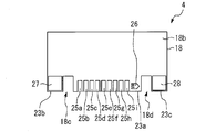
- FIGS. 4 and 5 are diagrams showing examples of the printed wiring board 4.
- the printed wiring board 4 includes, for example, an insulating substrate 18, a plurality of electrodes 19, pads 20, lands 21, and lands 22.
- the insulating substrate 18 is, for example, a plate having a constant thickness.
- a front surface 18a and a front surface 18b are formed on the insulating substrate 18.
- FIG. 4 is a diagram of the printed wiring board 4 as viewed from the front surface 18 a side of the insulating substrate 18.
- the electronic component 5 is arranged, for example, on the surface 18a side.
- the surface 18b faces in a direction opposite to the direction in which the surface 18a faces.
- the y-axis is parallel to surface 18a and surface 18b.
- the z-axis is parallel to the surface 18a and the surface 18b.
- the x-axis is orthogonal to surface 18a and surface 18b.
- the insulating substrate 18 includes, for example, a connection portion 23a, a connection portion 23b, and a connection portion 23c.
- the connection portion 23a, the connection portion 23b, and the connection portion 23c are provided on the insulating substrate 18 by, for example, forming the notch 18c and the notch 18d.
- connection portion 23a penetrates the mounting hole 15 from the front surface 6a side and protrudes from the front surface 6b of the insulating substrate 6.
- connection part 23 b penetrates the mounting hole 16 from the front surface 6 a side and protrudes from the front surface 6 b of the insulating substrate 6.
- connection portion 23c penetrates the mounting hole 17 from the front surface 6a side and protrudes from the front surface 6b of the insulating substrate 6.
- the printed wiring board 4 includes nine electrodes 19
- the number of electrodes 19 provided on the printed wiring board 4 is not limited to nine.
- reference numerals 19a to 19i are given when the electrodes 19 are individually specified.
- the electrodes 19a to 19i are provided on the surface 18a of the insulating substrate 18. Specifically, the electrodes 19a to 19i are provided on the surface 18a of the connection part 23a.
- the electrodes 19a to 19i constitute a part of a printed circuit formed on the insulating substrate 18.
- the electrodes 19a to 19i are arranged linearly in the y-axis direction.
- the electrodes 19a to 19i are arranged on the edge of the insulating substrate 18.
- the electrodes 19a to 19i are arranged at the connection part 23a.
- the electrode 19a is disposed at an end in the electrodes 19a to 19i arranged in a line.
- the electrode 19b is adjacent to the electrode 19a.
- the electrode 19c is adjacent to the electrode 19b.
- the electrode 19h is adjacent to the electrode 19g.
- the electrode 19i is adjacent to the electrode 19h.
- the electrode 19i is arranged at an end of the electrodes 19a to 19i arranged in a line.
- the pad 20 is provided on the surface 18 a of the insulating substrate 18. Specifically, the pad 20 is provided on the surface 18a of the connection part 23a. The pad 20 does not have to constitute a part of the printed circuit formed on the insulating substrate 18. For example, the pad 20 may not be electrically connected to the electrodes 19a to 19i. The electrodes 19a to 19i and the pad 20 are arranged in a line in the y-axis direction. The pad 20 is adjacent to the electrode 19i. The electrode 19i is arranged between the electrode 19h and the pad 20.
- the arrangement of the electrodes 19 and the pads 20 is the same as the arrangement of the electrodes 7 and the pads 8.
- the shape of the pad 20 is the same as the shape of the pad 8.
- the pad 20 includes, for example, a solder pool portion, a plurality of adjacent portions, and a terminal portion.
- the adjacent portion includes a portion adjacent to the electrode 19i.
- the adjacent portion linearly extends from the solder pool to the electrode 19i side.
- the adjacent portion is disposed between the electrode 19i and the solder pool. For example, three adjacent portions extend from the solder pool portion to the electrode 19i side.
- the end portion extends in the direction opposite to the direction in which the adjacent portion extends from the solder pool portion.
- the solder pool is disposed between the adjacent part and the terminal part.
- the terminal end is triangular.
- the width of the terminal end in the z-axis direction decreases as the distance from the electrode 19i increases.
- the land 21 and the land 22 are provided on the surface 18 a of the insulating substrate 18. Specifically, the land 21 is provided on the surface 18a of the connection part 23b. The land 22 is provided on the surface 18a of the connection part 23c. The land 21 and the land 22 do not have to constitute a part of a printed circuit formed on the insulating substrate 18.
- the land 21 is disposed so as to sandwich the notch 18c between the land 21 and the electrode 19a.
- the land 21 is arranged so that a part thereof is aligned with the electrodes 19 a to 19 i and the pad 20.
- the land 22 is arranged so as to sandwich the notch 18 d with the pad 20.
- the land 22 is arranged so that a part thereof is aligned with the electrodes 19a to 19i and the pad 20.
- FIG. 5 is a view of the printed wiring board 4 as viewed from the front surface 18b which is the back surface of the front surface 18a.
- the configuration of the front surface 18b of the printed wiring board 4 is the same as the configuration of the front surface 18a. That is, the printed wiring board 4 includes, for example, a plurality of electrodes 25, pads 26, lands 27, and lands 28.
- the printed wiring board 4 includes nine electrodes 25.
- the number of electrodes 25 provided on the printed wiring board 4 is not limited to nine.
- reference numerals 25a to 25i are given when the electrodes 25 are individually specified.
- the electrodes 25a to 25i are provided on the surface 18b of the insulating substrate 18. Specifically, the electrodes 25a to 25i are provided on the surface 18b of the connection part 23a.
- the electrodes 25a to 25i constitute a part of a printed circuit formed on the insulating substrate 18.
- the electrodes 25a to 25i are arranged linearly in the y-axis direction.
- the electrodes 25a to 25i are arranged on the edge of the insulating substrate 18.
- the electrodes 25a to 25i are arranged at the connection part 23a.
- the electrode 25a is arranged at an end in the electrodes 25a to 25i arranged in a line.
- the electrode 25b is adjacent to the electrode 25a.
- the electrode 25h is adjacent to the electrode 25g.
- the electrode 25i is adjacent to the electrode 25h.
- the electrode 25i is arranged at an end in the electrodes 25a to 25i arranged in a line.
- the pad 26 is provided on the surface 18 b of the insulating substrate 18. Specifically, the pad 26 is provided on the surface 18b of the connection part 23a. The pad 26 does not have to constitute a part of the printed circuit formed on the insulating substrate 18. For example, the pad 26 may not be electrically connected to the electrodes 25a to 25i. The electrodes 25a to 25i and the pads 26 are arranged in a line in the y-axis direction. The pad 26 is adjacent to the electrode 25i. The electrode 25i is arranged between the electrode 25h and the pad 26.
- the arrangement of the electrodes 25 and the pads 26 is the same as the arrangement of the electrodes 7 and the pads 8.
- the shape of the pad 26 is the same as the shape of the pad 8.
- the pad 26 includes, for example, a solder pool portion, a plurality of adjacent portions, and a terminal portion.
- the adjacent portion includes a portion adjacent to the electrode 25i.
- the adjacent portion linearly extends from the solder pool to the electrode 25i side.
- the adjacent portion is arranged between the electrode 25i and the solder pool. For example, three adjacent portions extend from the solder pool portion to the electrode 25i side.
- the end portion extends in the direction opposite to the direction in which the adjacent portion extends from the solder pool portion.
- the solder pool is disposed between the adjacent part and the terminal part.
- the terminal end is triangular.
- the width of the terminal end in the z-axis direction decreases as the distance from the electrode 25i increases.
- the land 27 and the land 28 are provided on the surface 18 b of the insulating substrate 18. Specifically, the land 27 is provided on the surface 18b of the connection part 23b. The land 28 is provided on the surface 18b of the connection part 23c. The lands 27 and lands 28 do not have to constitute a part of the printed circuit formed on the insulating substrate 18.
- the land 27 is arranged so as to sandwich the notch 18c with the electrode 25a.
- the land 27 is arranged so that a part thereof is aligned with the electrodes 25a to 25i and the pad 26.
- the land 28 is arranged so as to sandwich the notch 18 d with the pad 26.
- the land 28 is arranged so that a part thereof is aligned with the electrodes 25a to 25i and the pad 26.
- the printed circuit board 1 and the printed wiring board 4 configured as described above constitute the printed circuit board 1 as follows. That is, first, the printed wiring board 4 is disposed so as to be orthogonal to the printed wiring board 2. At this time, the connection portion 23a is passed through the mounting hole 15 from the front surface 6a side, and the connection portion 23a is projected from the front surface 6b of the insulating substrate 6. The connection portion 23b is passed through the mounting hole 16, and the connection portion 23b is projected from the front surface 6b of the insulating substrate 6. The connection portion 23c is passed through the mounting hole 17, and the connection portion 23c is projected from the front surface 6b of the insulating substrate 6.
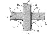
- FIG. 6 is a diagram showing a cross section taken along line AA of FIG.
- the electrode 7a is provided on the surface 6b of the insulating substrate 6.
- the electrode 19a is arranged so as to be adjacent to the electrode 7a provided on the insulating substrate 6.
- a solder 24 is provided between the electrode 19a and the electrode 7a.
- the electrode 19a is joined to the electrode 7a by the solder 24.
- the electrode 19b is arranged so as to be adjacent to the electrode 7b.
- the cross section including the electrode 19b and the electrode 7b is the same as the cross section shown in FIG.
- Solder 24 is provided between electrode 19b and electrode 7b.
- the electrode 19b is joined to the electrode 7b by the solder 24. Note that the electrode 19b and the electrode 19a are not connected by the solder 24.
- the electrodes 7b and 7a are not connected by the solder 24.
- the land 21 of the insulating substrate 18 is arranged so as to be adjacent to the land 11 of the insulating substrate 6.
- the cross section including the land 21 and the land 11 is similar to the cross section shown in FIG. Solder 24 is provided between land 21 and land 11. Land 21 is fixed to land 11 by solder 24.
- the lands 22 of the insulating substrate 18 are arranged so as to be adjacent to the lands 13 of the insulating substrate 6.
- the cross section including the land 22 and the land 13 is the same as the cross section shown in FIG. Solder 24 is provided between land 22 and land 13. Land 22 is fixed to land 13 by solder 24.
- the electrodes 25a to 25i of the insulating substrate 18 are arranged so as to be adjacent to the electrodes 9a to 9i provided on the insulating substrate 6.
- the electrode 25a is arranged so as to be adjacent to the electrode 9a provided on the insulating substrate 6.
- a solder 29 is provided between the electrode 25a and the electrode 9a.
- the electrode 25a is joined to the electrode 9a by the solder 29.
- the electrode 9a is provided on the surface 6b of the insulating substrate 6.
- the electrode 25b is arranged so as to be adjacent to the electrode 9b.
- the cross section including the electrode 25b and the electrode 9b is the same as the cross section shown in FIG.
- Solder 29 is provided between electrode 25b and electrode 9b. Electrode 25b is joined to electrode 9b by solder 29. Note that the electrode 25b and the electrode 25a are not connected by the solder 29. The electrode 9b and the electrode 9a are not connected by the solder 29.
- the lands 27 of the insulating substrate 18 are arranged adjacent to the lands 12 of the insulating substrate 6.
- the cross section including the land 27 and the land 12 is similar to the cross section shown in FIG. Solder 29 is provided between land 27 and land 12. Land 27 is fixed to land 12 by solder 29.
- the land 28 of the insulating substrate 18 is arranged so as to be adjacent to the land 14 of the insulating substrate 6.
- the cross section including the land 28 and the land 14 is the same as the cross section shown in FIG. Solder 29 is provided between land 28 and land 14. Land 28 is fixed to land 14 by solder 29.
- the insulating substrate 6 is an example of a first insulating substrate.
- a mounting hole 15 is formed in the insulating substrate 6, which is the first insulating substrate.
- the y-axis direction is a first direction
- the x-axis direction is a second direction
- the second direction is orthogonal to the first direction.
- the mounting hole 15 is a long hole whose width in the second direction is larger than that in the first direction.
- the surface 6a of the insulating substrate 6 is the first surface of the first insulating substrate.
- the surface 6b of the insulating substrate 6 is the second surface of the first insulating substrate.
- the insulating substrate 18 is an example of a second insulating substrate.
- the insulating substrate 18 serving as the second insulating substrate has a connection portion 23a that penetrates the mounting hole 15 from the surface 6a serving as the first surface and projects from the surface 6b serving as the second surface.
- the electrode 7 and the electrode 9 of the insulating substrate 6 are an example of the first electrode provided on the surface 6b which is the second surface described above.
- the electrodes 7 and 9 serving as the first electrodes are arranged at edges of the mounting hole 15 along the x-axis direction, that is, the second direction.
- the electrode 19 and the electrode 25 of the insulating substrate 18 are an example of a second electrode provided at the connection part 23a.
- the electrodes 19 and 25, which are the second electrodes, are joined to the first electrodes, that is, the electrodes 7 and 9, by solder 29.
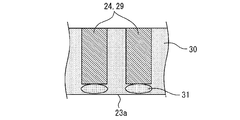
- the surface 6a and the surface 6b of the insulating substrate 6 are covered with the resist 30. However, the portions of each electrode including the electrodes 7 and 9 are not covered with the resist 30. Similarly, the surface 18 a and the surface 18 b of the insulating substrate 18 are covered with the resist 30. However, portions of each electrode including the electrode 19 and the electrode 25 are excluded. Therefore, as shown in FIG. 6, the resist 30 also exists on the distal end side of each of the electrode 19 and the electrode 25 in the connection portion 23a.
- a coating film 31 is provided on the connection portion 23a.
- the coating film 31 is provided by, for example, silk printing.
- the coating film 31 is provided by being applied on one or both surfaces of the second electrode (the electrode 19 and the electrode 25) of the connection portion 23a and the resist 30. Further, the coating film 31 is disposed at least on the tip side of the connection portion 23a with respect to the portion where the second electrodes (the electrodes 19 and 25) are soldered to the first electrodes (the electrodes 7 and 9).
- the printed wiring board 4 is disposed so as to be orthogonal to the printed wiring board 2.
- the connecting portion 23a is passed through the mounting hole 15 from the surface 6a side, and the connecting portion 23a is projected from the surface 6b of the insulating substrate 6.
- the connecting portion 23b is passed through the mounting hole 16 from the front surface 6a side, and the connecting portion 23b is projected from the front surface 6b of the insulating substrate 6.
- the connecting portion 23c is passed through the mounting hole 17 from the front surface 6a side, and the connecting portion 23c is projected from the front surface 6b of the insulating substrate 6.
- the printed wiring board 2 is fixed to the transfer device of the flow soldering device with the surface 6b facing downward.
- the printed wiring board 4 is placed upright on the printed wiring board 2 such that the connection portions 23a to 23c protrude downward from the printed wiring board 2.
- molten solder is ejected upward from a nozzle.
- the printed wiring board 2 and the printed wiring board 4 supported by the printed wiring board 2 are transported by the transport device and pass across the nozzles.
- the printed wiring board 2 passes above the nozzle, the lower surface of the printed wiring board 2 is immersed in the molten solder jetted from the nozzle. Further, a portion of the printed wiring board 4 protruding from the lower surface of the printed wiring board 2 is immersed in the molten solder jetted from the nozzle.
- the printed wiring board 2 is arranged so that the electrode 7a is immersed in the molten solder from the nozzle before the electrode 7i.
- the printed wiring board 2 is transported in the ⁇ y direction by the transport device. That is, the electrode 7i is immersed in the molten solder next to the electrode 7h, and the pad 8 is immersed in the molten solder after the electrode 7i.
- the printed wiring board 4 is arranged so that the electrode 19a is immersed in the molten solder from the nozzle before the electrode 19i. That is, the electrode 19i is immersed in the molten solder after the electrode 19h, and the pad 20 is immersed in the molten solder after the electrode 19i.
- the solder 24 is provided between the electrode 7a and the electrode 19a by immersing the electrode 7a and the electrode 19a in the molten solder from the nozzle.
- the solder 24 is provided between the electrode 7h and the electrode 19h by immersing the electrode 7h and the electrode 19h in the molten solder from the nozzle.
- the solder 24 is provided between the electrode 7i and the electrode 19i.
- the electrodes 7a to 7i are arranged so as to be arranged in a line in the direction of conveyance by the conveyance device. For this reason, the electrodes 7a to 7i are immersed in the molten solder from the nozzle in order from the electrode 7a.
- the pad 8 is immersed in the molten solder from the nozzle next to the electrode 7i.
- the electrodes 7a to 7i are separated from the molten solder from the nozzle in order from the electrode 7a.
- the pad 8 separates from the molten solder from the nozzle next to the electrode 7i.
- the pad 8 is not provided next to the electrode 7i, an excess amount of solder will remain on the electrode 7i when the molten solder separates from the electrode 7i. This causes a so-called bridge between the electrode 7h and the electrode 7i. That is, the electrode 7h and the electrode 7i are connected by solder.
- the pad 8 next to the electrode 7i the amount of solder remaining on the electrode 7i can be reduced to a required amount, and excess solder can be guided to the pad 8. That is, it is possible to prevent a bridge from being generated between the electrode 7h and the electrode 7i.
- connection portion 23a of the second electrode (the electrode 19 and the electrode 25) is smaller than the portion of the first electrode (the electrode 7 and the electrode 9) which is soldered. Is provided with a coating film 31 on the tip side. Then, due to the coating film 31, the thickness of the portion on the distal end side of the connection portion 23a becomes larger than the solder joint portion of the second electrode (the electrode 19 and the electrode 25). For this reason, more solder can be held on the second electrode (electrode 19 and electrode 25) above the coating film 31, and the solder of the second electrode (electrode 19 and electrode 25) is transferred from the tip side of the connection portion 23a to the solder bath.
- FIGS. 8 and 9 show examples of print patterns when the coating film 31 is provided for each of the second electrodes.
- the coating film 31 is formed between each second electrode (the electrode 19 and the electrode 25) and the tip of the connection portion 23a.
- the coating film 31 is provided on the surface of the resist 30 at the connection portion 23a. According to such a configuration example, during the flow soldering, the amount of solder taken from each second electrode (electrode 19 and electrode 25) into the solder bath can be reduced by each coating film 31.
- the coating film 31 is arranged in an arc shape at the tip of each of the second electrodes (the electrode 19 and the electrode 25).
- Each coating film 31 is convex on the tip side of the connection portion 23a and concave on the second electrode side.
- the coating film 31 is provided on both surfaces of the second electrode (the electrode 19 and the electrode 25) and the resist 30 of the connection portion 23a. According to such a configuration example, more solder can be held inside the concave portion of the arc-shaped coating film 31 during the flow soldering. Therefore, the amount of the molten solder adhering to the first electrode and the second electrode can be further increased.
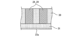
- 10 and 11 show examples of print patterns when at least a part of the coating film 31 is provided linearly along the arrangement direction of the second electrodes, that is, along the y-axis direction. That is, as shown in FIG. 10, the coating film 31 is formed linearly between each second electrode (the electrode 19 and the electrode 25) and the tip of the connection portion 23a. With such a configuration as well, the amount of solder taken from each of the second electrodes (electrodes 19 and 25) into the solder bath during flow soldering can be reduced by the linear coating film 31.
- the coating film 31 may be extended from a linear portion to a portion between the second electrodes (the electrode 19 and the electrode 25). By doing so, it is possible to suppress the occurrence of a bridge between the second electrodes (the electrode 19 and the electrode 25).
- the resist 30 is also provided on the distal end side of each of the electrode 19 and the electrode 25 in the connection portion 23a.
- the coating film 31 is basically applied on the surface of the second electrode (the electrode 19 and the electrode 25) of the connecting portion 23a.
- the end face on the distal end side of the connection portion 23 a is covered with the coating film 31.
- the both surfaces of the surface 18a and the surface 18b of the insulating substrate 18 can be formed. Can be formed once.
- FIG. 13 shows a configuration example in which the coating film 31 is linearly provided along the arrangement direction of the second electrodes, that is, the y-axis direction, over a plurality of second electrodes (the electrodes 19 and the electrodes 25).
- the amount of solder taken from each of the second electrodes (electrodes 19 and 25) into the solder bath during flow soldering can be reduced by the linear coating film 31.
- FIG. 14 shows an example in which an arc-shaped portion 31a is formed in the linear coating film 31 of the configuration example in FIG.
- the arc-shaped portion 31a is provided corresponding to each of the plurality of second electrodes (the electrode 19 and the electrode 25).
- Each arc-shaped portion 31a is convex on the tip side of the connecting portion 23a and concave on the second electrode side. According to such a configuration example, more solder can be held inside the concave portion of the arc-shaped portion 31a of the coating film 31 during flow soldering. Therefore, the amount of the molten solder adhering to the first electrode and the second electrode can be further increased.
- the present invention provides a printed circuit board having a plurality of insulating substrates, particularly a first insulating substrate having a mounting hole formed therein, and a second insulating substrate passing through the mounting hole of the first insulating substrate.
- the electrode of the second insulating substrate can be used for a printed circuit board joined by flow soldering.
Landscapes
- Engineering & Computer Science (AREA)
- Microelectronics & Electronic Packaging (AREA)
- Manufacturing & Machinery (AREA)
- Electric Connection Of Electric Components To Printed Circuits (AREA)
Abstract
Priority Applications (5)
| Application Number | Priority Date | Filing Date | Title |
|---|---|---|---|
| CA3107249A CA3107249C (fr) | 2018-07-26 | 2019-02-13 | Carte de circuit imprime |
| EP19841421.1A EP3829271A4 (fr) | 2018-07-26 | 2019-02-13 | Carte de circuit imprimé |
| US17/261,651 US11445609B2 (en) | 2018-07-26 | 2019-02-13 | Printed circuit board |
| JP2019533251A JP6583593B1 (ja) | 2018-07-26 | 2019-02-13 | プリント回路板 |
| CN201980046639.4A CN112425273B (zh) | 2018-07-26 | 2019-02-13 | 印刷电路板 |
Applications Claiming Priority (2)
| Application Number | Priority Date | Filing Date | Title |
|---|---|---|---|
| JP2018-140405 | 2018-07-26 | ||
| JP2018140405 | 2018-07-26 |
Publications (1)
| Publication Number | Publication Date |
|---|---|
| WO2020021742A1 true WO2020021742A1 (fr) | 2020-01-30 |
Family
ID=69181442
Family Applications (1)
| Application Number | Title | Priority Date | Filing Date |
|---|---|---|---|
| PCT/JP2019/005089 Ceased WO2020021742A1 (fr) | 2018-07-26 | 2019-02-13 | Carte de circuit imprimé |
Country Status (5)
| Country | Link |
|---|---|
| US (1) | US11445609B2 (fr) |
| EP (1) | EP3829271A4 (fr) |
| CN (1) | CN112425273B (fr) |
| CA (1) | CA3107249C (fr) |
| WO (1) | WO2020021742A1 (fr) |
Families Citing this family (2)
| Publication number | Priority date | Publication date | Assignee | Title |
|---|---|---|---|---|
| US11445609B2 (en) * | 2018-07-26 | 2022-09-13 | Mitsubishi Electric Corporation | Printed circuit board |
| JP7210186B2 (ja) * | 2018-08-07 | 2023-01-23 | タイコエレクトロニクスジャパン合同会社 | 回路基板組立体 |
Citations (3)
| Publication number | Priority date | Publication date | Assignee | Title |
|---|---|---|---|---|
| JP2004087748A (ja) * | 2002-08-27 | 2004-03-18 | Matsushita Electric Works Ltd | プリント配線板 |
| JP2008226964A (ja) * | 2007-03-09 | 2008-09-25 | Funai Electric Co Ltd | プリント配線基板の接続装置 |
| JP4314809B2 (ja) | 2002-10-31 | 2009-08-19 | パナソニック電工株式会社 | 複数のプリント基板を有する電子装置 |
Family Cites Families (9)
| Publication number | Priority date | Publication date | Assignee | Title |
|---|---|---|---|---|
| JPS60194367U (ja) * | 1984-06-01 | 1985-12-24 | 株式会社リコー | プリント配線基板 |
| US5455742A (en) * | 1994-03-21 | 1995-10-03 | Eaton Corporation | Direct circuit board connection |
| US6496384B1 (en) * | 2001-09-21 | 2002-12-17 | Visteon Global Technologies, Inc. | Circuit board assembly and method of fabricating same |
| EP1558064B1 (fr) | 2002-10-28 | 2014-07-09 | Panasonic Corporation | Dispositif d'actionnement d'une lampe a decharge haute pression et appareil d'eclairage comprenant ce dispositif |
| JP5009972B2 (ja) | 2009-12-21 | 2012-08-29 | 日立オートモティブシステムズ株式会社 | コネクタの製造方法 |
| JP5904856B2 (ja) * | 2012-04-23 | 2016-04-20 | キヤノン株式会社 | プリント配線板、半導体パッケージ及びプリント回路板 |
| WO2017209168A1 (fr) | 2016-06-03 | 2017-12-07 | 有限会社笠井建築設計コンサルタント | Structure de connexion de fils pour carte à circuits imprimés à âme métallique, carte à circuits imprimés à âme métallique, et procédé pour sa fabrication |
| JP6729147B2 (ja) * | 2016-08-03 | 2020-07-22 | 三菱電機株式会社 | プリント回路板 |
| US11445609B2 (en) * | 2018-07-26 | 2022-09-13 | Mitsubishi Electric Corporation | Printed circuit board |
-
2019
- 2019-02-13 US US17/261,651 patent/US11445609B2/en active Active
- 2019-02-13 CN CN201980046639.4A patent/CN112425273B/zh not_active Expired - Fee Related
- 2019-02-13 EP EP19841421.1A patent/EP3829271A4/fr not_active Withdrawn
- 2019-02-13 WO PCT/JP2019/005089 patent/WO2020021742A1/fr not_active Ceased
- 2019-02-13 CA CA3107249A patent/CA3107249C/fr active Active
Patent Citations (3)
| Publication number | Priority date | Publication date | Assignee | Title |
|---|---|---|---|---|
| JP2004087748A (ja) * | 2002-08-27 | 2004-03-18 | Matsushita Electric Works Ltd | プリント配線板 |
| JP4314809B2 (ja) | 2002-10-31 | 2009-08-19 | パナソニック電工株式会社 | 複数のプリント基板を有する電子装置 |
| JP2008226964A (ja) * | 2007-03-09 | 2008-09-25 | Funai Electric Co Ltd | プリント配線基板の接続装置 |
Also Published As
| Publication number | Publication date |
|---|---|
| US11445609B2 (en) | 2022-09-13 |
| CA3107249C (fr) | 2023-06-13 |
| EP3829271A1 (fr) | 2021-06-02 |
| EP3829271A4 (fr) | 2021-09-29 |
| CN112425273A (zh) | 2021-02-26 |
| CA3107249A1 (fr) | 2020-01-30 |
| US20210267060A1 (en) | 2021-08-26 |
| CN112425273B (zh) | 2023-11-14 |
Similar Documents
| Publication | Publication Date | Title |
|---|---|---|
| WO2021235196A1 (fr) | Structure de montage pour composant de puce | |
| WO2020021742A1 (fr) | Carte de circuit imprimé | |
| JP6583593B1 (ja) | プリント回路板 | |
| JP6729147B2 (ja) | プリント回路板 | |
| JP2002280717A (ja) | プリント基板 | |
| JP5576757B2 (ja) | プリント基板 | |
| CN113545174A (zh) | 印刷布线板以及电子设备 | |
| JP7110610B2 (ja) | プリント回路板 | |
| JP2000252613A (ja) | 電子回路基板及びその半田付け方法 | |
| JP2020178106A (ja) | 電子機器、電子機器の製造方法、プリント基板、プリント基板の製造方法 | |
| JP2926956B2 (ja) | プリント基板 | |
| JPH06204652A (ja) | プリント回路基板 | |
| JP2019140327A (ja) | プリント配線板、プリント回路板およびプリント回路板の製造方法 | |
| JP7069404B2 (ja) | プリント配線板および電子機器 | |
| JPH0383393A (ja) | プリント配線板 | |
| JP2554693Y2 (ja) | プリント基板 | |
| JP2001119119A (ja) | 印刷回路基板及び電子部品の実装方法 | |
| JP2000312074A (ja) | プリント基板 | |
| JP2005317691A (ja) | プリント基板のはんだ付け方法及びはんだ付けに用いるパレット | |
| JPH02258161A (ja) | 噴流式半田槽 | |
| JPH0794857A (ja) | プリント配線板 | |
| JPH04291988A (ja) | 両面smtプリント基板構造及び両面smtプリント基板に於けるリフロー半田付け方法 | |
| JPH0774461A (ja) | 電子部品の半田付け方法およびその半田付け方法に用いられるスクリ−ンマスク | |
| JPH01119085A (ja) | プリント板 | |
| JP2000269628A (ja) | リフローによるチップ部品の取付構造、並びにリフローによるチップ部品の取付方法 |
Legal Events
| Date | Code | Title | Description |
|---|---|---|---|
| ENP | Entry into the national phase |
Ref document number: 2019533251 Country of ref document: JP Kind code of ref document: A |
|
| 121 | Ep: the epo has been informed by wipo that ep was designated in this application |
Ref document number: 19841421 Country of ref document: EP Kind code of ref document: A1 |
|
| ENP | Entry into the national phase |
Ref document number: 3107249 Country of ref document: CA |
|
| NENP | Non-entry into the national phase |
Ref country code: DE |
|
| WWE | Wipo information: entry into national phase |
Ref document number: 2019841421 Country of ref document: EP |