WO2021111966A1 - 金属片付き配線基板 - Google Patents
金属片付き配線基板 Download PDFInfo
- Publication number
- WO2021111966A1 WO2021111966A1 PCT/JP2020/043952 JP2020043952W WO2021111966A1 WO 2021111966 A1 WO2021111966 A1 WO 2021111966A1 JP 2020043952 W JP2020043952 W JP 2020043952W WO 2021111966 A1 WO2021111966 A1 WO 2021111966A1
- Authority
- WO
- WIPO (PCT)
- Prior art keywords
- metal piece
- wiring board
- welded portion
- welded
- wiring layer
- Prior art date
- Legal status (The legal status is an assumption and is not a legal conclusion. Google has not performed a legal analysis and makes no representation as to the accuracy of the status listed.)
- Ceased
Links
Images








Classifications
-
- B—PERFORMING OPERATIONS; TRANSPORTING
- B23—MACHINE TOOLS; METAL-WORKING NOT OTHERWISE PROVIDED FOR
- B23K—SOLDERING OR UNSOLDERING; WELDING; CLADDING OR PLATING BY SOLDERING OR WELDING; CUTTING BY APPLYING HEAT LOCALLY, e.g. FLAME CUTTING; WORKING BY LASER BEAM
- B23K26/00—Working by laser beam, e.g. welding, cutting or boring
- B23K26/20—Bonding
- B23K26/21—Bonding by welding
-
- H—ELECTRICITY
- H05—ELECTRIC TECHNIQUES NOT OTHERWISE PROVIDED FOR
- H05K—PRINTED CIRCUITS; CASINGS OR CONSTRUCTIONAL DETAILS OF ELECTRIC APPARATUS; MANUFACTURE OF ASSEMBLAGES OF ELECTRICAL COMPONENTS
- H05K1/00—Printed circuits
- H05K1/02—Details
- H05K1/14—Structural association of two or more printed circuits
-
- H—ELECTRICITY
- H05—ELECTRIC TECHNIQUES NOT OTHERWISE PROVIDED FOR
- H05K—PRINTED CIRCUITS; CASINGS OR CONSTRUCTIONAL DETAILS OF ELECTRIC APPARATUS; MANUFACTURE OF ASSEMBLAGES OF ELECTRICAL COMPONENTS
- H05K3/00—Apparatus or processes for manufacturing printed circuits
- H05K3/30—Assembling printed circuits with electric components, e.g. with resistors
- H05K3/32—Assembling printed circuits with electric components, e.g. with resistors electrically connecting electric components or wires to printed circuits
Definitions
- the present invention relates to a wiring board with a metal piece.
- the present application claims priority based on Japanese Patent Application No. 2019-220318 filed in Japan on December 5, 2019, the contents of which are incorporated herein by reference.
- Patent Document 1 discloses a structure in which a flexible circuit board and a bus bar are joined by welding.
- One aspect of the present invention is to provide a wiring board with a metal piece that is less likely to crack in a welded portion.
- One aspect of the present invention includes a wiring substrate having a coverlay having an opening and a wiring layer having a through hole, and a metal piece, and the through hole overlaps the opening in a plan view.
- the metal piece has a welded portion and a non-welded portion joined to the wiring layer at a portion facing the wiring layer through the opening, and the welded portion is a peripheral edge of the through hole.
- a wiring substrate with a metal piece which is formed in an annular shape along the portion so as to surround the non-welded portion.
- the melted portion of the metal piece during welding is formed in an annular shape, and the central portion does not melt, so that stress concentration is less likely to occur during solidification as compared with the case where the entire circular region is melted. Therefore, it is possible to suppress the occurrence of cracks in the welded portion due to stress concentration during solidification.
- FIG. 4 is a cross-sectional view taken along the line II shown in FIG. It is a photograph of the welded part of an example of a wiring board with a metal piece. It is a photograph of the cross section of the welded portion shown in FIG. It is explanatory drawing of the manufacturing method of the wiring board with a metal piece of embodiment.
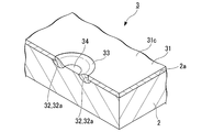
- FIG. 1 is a perspective view of the wiring board 3 with a metal piece according to the embodiment.
- FIG. 2 is an enlarged perspective view showing a wiring board 3 with a metal piece, and is a diagram showing a partial cross section of the wiring board 3 with a metal piece.
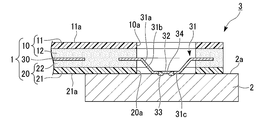
- FIG. 3 is a cross-sectional view of the wiring board 3 with a metal piece.
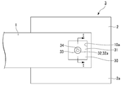
- FIG. 4 is a plan view of the wiring board 3 with a metal piece.
- FIG. 5 is a cross-sectional view taken along the line II of FIG.
- the wiring board 3 with a metal piece includes a flexible printed circuit board (FPC) 1 and a metal piece 2.
- FPC flexible printed circuit board
- the flexible printed circuit board 1 has a first cover ray 10, a second cover ray 20, and a wiring layer 30 (metal layer).
- the flexible printed circuit board 1 has flexibility.
- the flexible printed circuit board 1 is configured so that the wiring layer 30 functions even when it is greatly bent.
- the flexible printed circuit board 1 is an example of a “wiring board”.
- the wiring board is not limited to the flexible printed circuit board, but may be a rigid board.
- the rigid substrate is a wiring substrate including a rigid substrate such as a glass epoxy substrate or a glass substrate, and a wiring layer.
- the thickness direction of the flexible printed circuit board 1 is simply referred to as the thickness direction. Further, the direction from the metal piece 2 toward the flexible printed circuit board 1 along the thickness direction is referred to as an upper direction, and the opposite direction is referred to as a lower direction. Viewing from the top and bottom is called plan view.
- the first coverlay 10 has a first insulator 11 and a first adhesive layer 12 applied to the first insulator 11.
- the second coverlay 20 has a second insulator 21 and a second adhesive layer 22 applied to the second insulator 21.
- the flexible printed circuit board 1 has a laminated structure in which the second cover ray 20, the wiring layer 30, and the first cover ray 10 are laminated in this order from the bottom to the top.
- the first insulator 11 is located on the uppermost layer of the flexible printed circuit board 1
- the second insulator 21 is located on the lowermost layer of the flexible printed circuit board 1.
- the first insulator 11 and the second insulator 21 are formed in a thin film shape.
- flexible and insulating materials can be used.
- the materials of the insulators 11 and 21 include polyimide and liquid crystal polymer.
- a polyimide film having a thickness of 25 ⁇ m is used as the insulators 11 and 21.
- the first adhesive layer 12 adheres the wiring layer 30 and the first insulator 11.
- the second adhesive layer 22 adheres the wiring layer 30 and the second insulator 21.
- a resin having an insulating property and an adhesive property can be used as the material of the adhesive layers 12 and 22.
- the resin having insulating property and adhesiveness include epoxy-based, acrylic-based, and polyimide-based resins.
- an epoxy adhesive having a thickness of 25 ⁇ m is used as the adhesive layers 12 and 22.
- a first opening 10a is formed in the first coverlay 10.
- a second opening 20a (opening) is formed in the second coverlay 20.
- the openings 10a and 20a can be formed by subjecting the coverlays 10 and 20 to laser processing, mold processing, NC processing (Numerical Control machining) and the like.
- the first opening 10a and the second opening 20a are arranged at positions where they overlap each other when viewed from the thickness direction.
- the first opening 10a and the second opening 20a are formed in a square shape.
- the first opening 10a and the second opening 20a have the same shape. The shapes, sizes, arrangements, etc. of the openings 10a and 20a may be changed as appropriate.
- the wiring layer 30 (wiring pattern) is sandwiched between the first cover ray 10 and the second cover ray 20.
- a thin metal film having conductivity can be used.
- the material of the wiring layer 30 include copper, stainless steel, and aluminum.
- the melting point of the material of the wiring layer 30 is preferably higher than the melting point of the material of the metal piece 2.
- an electrolytic copper foil having a thickness of 35 ⁇ m is used as the wiring layer 30.
- the wiring layer 30 can be formed by, for example, a subtractive method, a semi-additive method, or the like.
- the portion of the wiring layer 30 exposed from the first cover lay 10 and the second cover lay 20 through the openings 10a and 20a is referred to as an exposed portion 31.
- a part of the exposed portion 31 is formed in a concave shape downward (that is, toward the metal piece 2).
- the portion deformed in a concave shape toward the metal piece 2 is referred to as a concave deformed portion 31a.
- the concave deformed portion 31a has a reduced diameter portion 31b and a bottom portion 31c.
- the diameter-reduced portion 31b is reduced in diameter downward.
- the cross-sectional shape of the reduced diameter portion 31b orthogonal to the thickness direction is, for example, a circular shape.
- the bottom portion 31c is formed at the lower end of the reduced diameter portion 31b.
- the bottom portion 31c is formed in a disk shape, for example.
- the bottom portion 31c is in contact with the first main surface 2a of the metal piece 2.
- the shape of the concave deformed portion 31a is, for example, a truncated cone shape whose diameter is reduced downward.
- a through hole 32 is formed in the center of the bottom portion 31c.
- the shape of the through hole 32 is a circular shape (see FIGS. 2 and 4).
- the through hole 32 is located at a position overlapping the second opening 20a.
- the inner diameter of the through hole 32 is smaller than the inner diameter of the second opening 20a.
- the through hole 32 is included in the second opening 20a.
- the bottom portion 31c is joined to the metal piece 2 by a welded portion 33 (joining portion) described later.
- the bottom portion 31c is electrically connected to the metal piece 2 by the welded portion 33.
- the electronic component may be a capacitor, a resistor, a thermistor, an IC, an LED, or the like.
- the first coverlay 10 or the second coverlay 20 may be provided with an opening for electrically connecting the electronic component and the wiring layer 30.
- the metal piece 2 is formed of a metal such as aluminum or an aluminum alloy into a plate shape, a film shape, a rod shape, or the like. The material and shape of the metal piece 2 may be changed as appropriate.
- the metal piece 2 may be made of copper, a copper alloy, or the like.
- an aluminum plate (A1050) having a thickness of 1 mm is used as the metal piece 2.
- the upper surface of the metal piece 2 is a first main surface 2a facing the flexible printed circuit board 1.
- the metal piece 2 covers the second opening 20a of the second insulator 21 from below.
- the metal piece 2 is eutectic with a welded portion 33, a non-welded portion 34 (non-joined portion), and a portion facing the wiring layer 30 through the second opening 20a (see FIG. 3). It has a part 35 and the like.
- the welded portion 33 and the non-welded portion 34 are formed in a region including at least the first main surface 2a.
- the welded portion 33 is a portion where the metal piece 2 is melted and then solidified by heating during welding in the joining step described later. That is, the welded portion 33 is a portion having a melting history.
- the welded portion 33 is formed in an annular shape along the peripheral edge portion 32a of the through hole 32 (see FIGS. 2 and 4).
- a part of the welded portion 33 (specifically, the annular outer peripheral portion 33a including the outer peripheral edge of the welded portion 33) is the bottom portion 31c of the wiring layer 30 (specifically, the annular inner peripheral portion 31d including the peripheral edge portion 32a). Located below.
- the inner peripheral portion 31d of the bottom portion 31c covers the outer peripheral portion 33a of the welded portion 33 from above.
- the inner peripheral portion 31d is joined to the outer peripheral portion 33a.
- the welding area between the wiring layer 30 and the metal piece 2 becomes large, and the welding strength can be increased.
- the portion (inner peripheral portion 33b) excluding the outer peripheral portion 33a (the portion overlapping the bottom portion 31c) is inside the through hole 32 in a plan view.
- the inner diameter of the welded portion 33 is smaller than the inner diameter of the through hole 32.
- the welded portion 33 surrounds the non-welded portion 34 on the first main surface 2a (see FIGS. 2 and 4).
- a part of the welded portion 33 bulges upward on the first main surface 2a. This portion is called a bulging portion 33c.
- the bulging portion 33c is an annular portion protruding upward with respect to the surface of the non-welded portion 34.
- the outer peripheral surface of the bulging portion 33c is joined to the inner peripheral surface of the peripheral edge portion 32a.
- the non-welded portion 34 is a portion that has not been melted by heating during welding for joining the wiring layer 30 to the metal piece 2. That is, the non-welded portion 34 is a portion having no melting history.
- the non-welded portion 34 surrounded by the welded portion 33 has a circular shape in a plan view (see FIGS. 2 and 4).
- the eutectic portion 35 is formed at the interface between the bottom portion 31c of the wiring layer 30 and the metal piece 2.
- the eutectic portion 35 is, for example, a portion where the bottom portion 31c and the metal piece 2 are melted and mixed and solidified in a eutectic state.
- the eutectic portion 35 is formed from the inner peripheral surface of the through hole 32 of the bottom portion 31c to the lower surface of the inner peripheral portion 31d.
- the eutectic portion 35 can be said to be an alloy layer (or an intermetallic compound layer) composed of the constituent metal of the wiring layer 30 and the constituent metal of the metal piece 2.
- the shapes of the welded portion 33, the non-welded portion 34, and the eutectic portion 35 are confirmed by observing the cut surfaces of each part of the welded portion 33, the non-welded portion 34, and the eutectic portion 35, X-ray imaging, and the like. be able to.
- FIG. 6 is a photograph of the welded portion 33 of an example of the wiring board 3 with a metal piece seen from above.
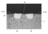
- FIG. 7 is a photograph of a cross section of the welded portion 33. As shown in FIGS. 6 and 7, the welded portion 33 is formed in an annular shape so as to surround the non-welded portion 34.
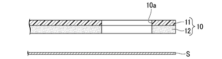
- the preparation step is a step of preparing the flexible printed circuit board 1. As shown in FIG. 8, in the preparation step, the first coverlay 10 and the conductor sheet S are prepared. A first opening 10a is formed in advance in the first coverlay 10. The first adhesive layer 12 of the first coverlay 10 is in a semi-cured state.
- the sheet S is a metal foil made of copper, stainless steel, aluminum, or the like.
- the first coverlay 10 and the seat S are aligned so as to face each other.
- the first coverlay 10 and the sheet S are laminated and integrated by a heating press.
- the first adhesive layer 12 is cured, and the first coverlay 10 and the sheet S are fixed.
- the conditions of the heating press are preferably in the range of, for example, a temperature of 100 to 200 ° C., a pressure of 0.1 to 10 MPa, and a pressurization time of 1 to 120 minutes. If necessary, the first coverlay 10 and the sheet S may be heated in an oven after the heating press.
- the sheet S integrated with the first coverlay 10 is processed to form the wiring layer 30.
- the wiring layer 30 can be obtained by a subtractive method or laser processing.
- the subtractive method is adopted, and the wiring layer 30 is formed by etching the sheet S.
- a through hole 32 is formed in the portion of the wiring layer 30 exposed from the first opening 10a (exposed portion 31).
- the shape of the through hole 32 is a circular shape (see FIG. 2).
- the second coverlay 20 is arranged below the wiring layer 30.
- a second opening 20a is formed in advance in the second coverlay 20.
- the first cover lay 10 and the wiring layer 30 and the second cover lay 20 are positioned and laminated, and integrated by a heating press.
- the second adhesive layer 22 is cured, and the members 10, 20, and 30 are fixed (see FIG. 12).
- the conditions for the heating press may be the same as when the first coverlay 10 and the sheet S are integrated.
- the metal piece 2 is arranged below the integrated first cover ray 10, the wiring layer 30, and the second cover ray 20.
- a part of the exposed portion 31 of the wiring layer 30 and the metal piece 2 are joined (joining step).
- a concave deformed portion 31a is formed in a part of the exposed portion 31.
- a joining method laser welding, resistance welding and the like can be used.
- the laser beam L is emitted downward from the welding laser device 40 to irradiate the exposed portion 31 and the metal piece 2 of the wiring layer 30 (irradiation step).
- the irradiation region of the laser beam L may be, for example, an annular region concentric with the through hole 32 in a plan view.
- the inner diameter of the irradiation region is smaller than the inner diameter of the through hole 32, and the outer diameter of this irradiation region is larger than the inner diameter of the through hole 32.
- the locus (trajectory pattern) of the laser beam L in the irradiation region is not particularly limited, and may be, for example, a wobbling shape, a spiral shape, a plurality of concentric circles, or the like.
- the annular portion of the metal piece 2 along the peripheral edge portion 32a melts and then solidifies.
- the welded portion 33 (see FIG. 5) is formed.
- the portion of the metal piece 2 that has not been melted becomes the non-welded portion 34.
- a part of the bottom portion 31c is joined to the metal piece 2 by the welded portion 33.
- a eutectic portion 35 (see FIG. 5) is formed at the interface between a part of the bottom portion 31c and the metal piece 2.
- the electronic component may be mounted on the flexible printed circuit board 1 before or after joining the wiring layer 30 to the metal piece 2.
- the welded portion 33 for joining the wiring layer 30 to the metal piece 2 is formed in an annular shape along the peripheral edge portion 32a of the through hole 32 so as to surround the non-welded portion 34. .. Since the molten portion of the metal piece 2 during welding is formed in an annular shape and the central portion does not melt, stress concentration is less likely to occur during solidification as compared with the case where the entire circular region is melted. Therefore, it is possible to suppress the occurrence of cracks in the welded portion 33 due to stress concentration during solidification.
- FIG. 18 is a photograph of a cross section of a welded portion 133 of a wiring board with a metal piece in a comparative form.
- the welded portion 133 is formed by melting the entire circular region of the metal piece, not the annular shape.
- a crack C is formed in the welded portion 133 at a position close to the central portion. It can be inferred that this crack C was generated by the concentration of stress in the central portion of the melted portion during solidification.
- the welded portion 33 is formed in an annular shape, it is easy to judge the quality of welding based on the shape of the welded portion 33. Further, as shown in FIG. 5, in the wiring board 3 with a metal piece, the welded portion 33 is formed in contact with the wiring layer 30 in a wide region from the inner peripheral surface of the through hole 32 to the lower surface of the bottom portion 31c. The connection reliability between the layer 30 and the metal piece 2 can be improved.
- the processing time can be shortened.
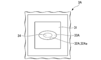
- FIG. 14 is a plan view of a part of the wiring board 3A with a metal piece having the welded portion 33A of the first modification.
- the through hole 32A has an elliptical shape in a plan view.
- the weld 33A is formed in an elliptical ring along the peripheral edge 32Aa of the through hole 32A.
- the welded portion 33A surrounds the non-welded portion 34.
- the elliptical annular welded portion 33A can be appropriately adopted in accordance with the space in which the welded portion is formed in the wiring layer 30 and the metal piece 2.
- FIG. 15 is a plan view of a part of the wiring board 3B with a metal piece having the welded portion 33B of the second modification.
- the through hole 32B is formed in a rectangular shape in a plan view.
- the welded portion 33B is formed in a rectangular ring shape along the peripheral edge portion 32Ba of the through hole 32B.
- the welded portion 33B surrounds the non-welded portion 34.
- the rectangular annular welded portion 33A can be appropriately adopted in accordance with the space in which the welded portion is formed in the wiring layer 30 and the metal piece 2.
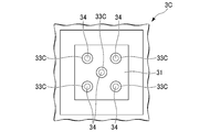
- FIG. 16 is a plan view of a part of the wiring board 3C with a metal piece having the welded portion 33C of the third modification.
- a plurality of welded portions 33C formed in an annular shape are formed similarly to the welded portions 33 shown in FIGS. 1 and 2. Since a plurality of welded portions 33C are formed on the metal piece-attached wiring board 3C, the welding strength can be increased. Since a plurality of welded portions 33C are formed on the wiring board 3C with a metal piece, the electrical resistance of the welded portion can be reduced.
- FIG. 17 is a plan view of a part of the wiring board 3D with a metal piece having the welded portion 33D of the fourth modification.
- a plurality of welded portions 33D are formed in the wiring board 3D with a metal piece.
- the plurality of welded portions 33D include an annular welded portion 33D1 and a rectangular annular welded portion 33D2. Since a plurality of welded portions 33D1 and 33D2 are formed on the wiring board 3D with a metal piece, the welding strength can be increased.
Landscapes
- Engineering & Computer Science (AREA)
- Microelectronics & Electronic Packaging (AREA)
- Physics & Mathematics (AREA)
- Optics & Photonics (AREA)
- Manufacturing & Machinery (AREA)
- Plasma & Fusion (AREA)
- Mechanical Engineering (AREA)
- Structure Of Printed Boards (AREA)
Abstract
本発明の金属片付き配線基板は、開口部が形成されたカバーレイおよび貫通孔が形成された配線層を有する配線基板と、金属片とを備える。平面視において、前記貫通孔は前記開口部と重なっている。前記金属片は、前記開口部を通して前記配線層に対向する部分に、前記配線層に接合された溶接部と、非溶接部とを有する。前記溶接部は、前記貫通孔の周縁部に沿って前記非溶接部を囲むように環状に形成されている。
Description
本発明は、金属片付き配線基板に関する。
本願は、2019年12月5日に日本に出願された特願2019-220318号に基づき優先権を主張し、その内容をここに援用する。
本願は、2019年12月5日に日本に出願された特願2019-220318号に基づき優先権を主張し、その内容をここに援用する。
特許文献1には、フレキシブル回路基板と、バスバーとが溶接により接合された構造が開示されている。
しかしながら、特許文献1に記載の構造では、溶接箇所において冷却時に凝固割れが生じる可能性があった。
本発明の一態様は、溶接部において割れが生じにくい金属片付き配線基板を提供することを目的とする。
本発明の一態様は、開口部が形成されたカバーレイおよび貫通孔が形成された配線層を有する配線基板と、金属片と、を備え、平面視において、前記貫通孔は前記開口部と重なっており、前記金属片は、前記開口部を通して前記配線層に対向する部分に、前記配線層に接合された溶接部と、非溶接部とを有し、前記溶接部は、前記貫通孔の周縁部に沿って前記非溶接部を囲むように環状に形成されている、金属片付き配線基板を提供する。
この構成によれば、溶接時における金属片の溶融箇所は環状に形成されており、中央部は溶融しないため、円形領域の全体を溶融させる場合に比べ、凝固時に応力集中が起こりにくい。よって、凝固時の応力集中を原因とする溶接部の割れ(クラック)発生を抑えることができる。
本発明の一態様によれば、溶接部において割れが生じにくい金属片付き配線基板を提供することができる。
以下、本実施形態の金属片付き配線基板について図面に基づいて説明する。
[金属片付き配線基板]
図1は、実施形態の金属片付き配線基板3の斜視図である。図2は、金属片付き配線基板3を示す拡大斜視図であって、金属片付き配線基板3の一部の断面を示す図である。図3は、金属片付き配線基板3の断面図である。図4は、金属片付き配線基板3の平面図である。図5は、図4のI-I断面図である。
[金属片付き配線基板]
図1は、実施形態の金属片付き配線基板3の斜視図である。図2は、金属片付き配線基板3を示す拡大斜視図であって、金属片付き配線基板3の一部の断面を示す図である。図3は、金属片付き配線基板3の断面図である。図4は、金属片付き配線基板3の平面図である。図5は、図4のI-I断面図である。
図1および図4に示すように、金属片付き配線基板3は、フレキシブルプリント基板(FPC:Flexible Printed Circuit)1と、金属片2と、を備えている。
図3に示すように、フレキシブルプリント基板1は、第1カバーレイ10と、第2カバーレイ20と、配線層30(金属層)と、を有している。フレキシブルプリント基板1は、可撓性を有する。フレキシブルプリント基板1は、大きく撓ませた場合にも配線層30が機能するように構成されている。フレキシブルプリント基板1は、「配線基板」の一例である。
なお、配線基板は、フレキシブルプリント基板に限らず、リジッド基板であってもよい。リジッド基板は、ガラスエポキシ基材、ガラス基材等のリジッドな基材と、配線層とを備えた配線基板である。
(方向定義)
本実施形態では、フレキシブルプリント基板1の厚さ方向を、単に厚さ方向という。また、厚さ方向に沿って、金属片2からフレキシブルプリント基板1に向かう方向を上方といい、その反対方向を下方という。上下方向から見ることを平面視という。
本実施形態では、フレキシブルプリント基板1の厚さ方向を、単に厚さ方向という。また、厚さ方向に沿って、金属片2からフレキシブルプリント基板1に向かう方向を上方といい、その反対方向を下方という。上下方向から見ることを平面視という。
(フレキシブルプリント基板)
第1カバーレイ10は、第1絶縁体11と、第1絶縁体11に塗布された第1接着層12と、を有している。第2カバーレイ20は、第2絶縁体21と、第2絶縁体21に塗布された第2接着層22と、を有している。
フレキシブルプリント基板1は、下から上に向かって、第2カバーレイ20、配線層30、第1カバーレイ10の順に積層された積層構造を有している。第1絶縁体11は、フレキシブルプリント基板1の最上層に位置し、第2絶縁体21は、フレキシブルプリント基板1の最下層に位置している。
第1カバーレイ10は、第1絶縁体11と、第1絶縁体11に塗布された第1接着層12と、を有している。第2カバーレイ20は、第2絶縁体21と、第2絶縁体21に塗布された第2接着層22と、を有している。
フレキシブルプリント基板1は、下から上に向かって、第2カバーレイ20、配線層30、第1カバーレイ10の順に積層された積層構造を有している。第1絶縁体11は、フレキシブルプリント基板1の最上層に位置し、第2絶縁体21は、フレキシブルプリント基板1の最下層に位置している。
第1絶縁体11および第2絶縁体21は、薄膜状に形成されている。絶縁体11、21としては、可撓性および絶縁性のある材質を使用することができる。絶縁体11、21の材質としては、例えば、ポリイミド、液晶ポリマー等が挙げられる。本実施形態では、絶縁体11、21として、厚さ25μmのポリイミドフィルムが用いられている。
第1接着層12は、配線層30と第1絶縁体11とを接着している。第2接着層22は、配線層30と第2絶縁体21とを接着している。接着層12、22の材質としては、絶縁性および接着性を有する樹脂を用いることができる。絶縁性および接着性を有する樹脂としては、エポキシ系、アクリル系、ポリイミド系等が挙げられる。本実施形態では、接着層12、22として、厚さ25μmのエポキシ系接着剤が用いられている。
第1カバーレイ10には、第1開口部10aが形成されている。第2カバーレイ20には、第2開口部20a(開口部)が形成されている。開口部10a、20aは、カバーレイ10、20にレーザー加工、金型加工、NC加工(Numerical Control machining)などを施すことで形成することができる。第1開口部10aおよび第2開口部20aは、厚さ方向から見て、互いに重なる位置に配置されている。第1開口部10aおよび第2開口部20aは、正方形状に形成されている。第1開口部10aおよび第2開口部20aは、同じ形状とされている。なお、開口部10a、20aの形状、大きさ、配置などは適宜変更してもよい。
配線層30(配線パターン)は、第1カバーレイ10および第2カバーレイ20に挟まれている。配線層30としては、導電性を有する金属の薄膜を用いることができる。配線層30の材質としては、例えば銅、ステンレス、アルミニウム等が挙げられる。配線層30の材質の融点は、金属片2の材質の融点より高いことが好ましい。本実施形態では、配線層30として、厚さ35μmの電解銅箔が用いられている。配線層30は、例えば、サブトラクティブ法、セミアディティブ法などにより形成することができる。
配線層30のうち、開口部10a、20aを通して第1カバーレイ10および第2カバーレイ20から露出した部分を露出部31という。露出部31の一部は、下方に向けて(すなわち、金属片2に向けて)凹状に形成されている。露出部31のうち、金属片2に向けて凹状に変形された部分を凹状変形部31aという。
凹状変形部31aは、縮径部31bと、底部31cとを有する。縮径部31bは、下方に向けて縮径する。厚さ方向に直交する縮径部31bの断面の形状は、例えば円形状である。底部31cは、縮径部31bの下端に形成されている。底部31cは、例えば、円板状に形成されている。底部31cは、金属片2の第1主面2aに当接している。凹状変形部31aの形状は、例えば、下方に向けて縮径する円錐台形状である。
底部31cの中央には、貫通孔32が形成されている。本実施形態では、貫通孔32の形状は、円形状である(図2および図4参照)。平面視において、貫通孔32は、第2開口部20aと重なる位置にある。貫通孔32の内径は、第2開口部20aの内径より小さい。平面視において、貫通孔32は、第2開口部20aに包含される。
底部31cは、後述する溶接部33(接合部)によって金属片2に接合されている。底部31cは、溶接部33によって金属片2と電気的に接続されている。
底部31cは、後述する溶接部33(接合部)によって金属片2に接合されている。底部31cは、溶接部33によって金属片2と電気的に接続されている。
図示は省略するが、フレキシブルプリント基板1には、電子部品が実装されていてもよい。電子部品は、コンデンサ、抵抗、サーミスタ、IC、LED等であってもよい。電子部品を実装する場合、第1カバーレイ10または第2カバーレイ20に、電子部品と配線層30とを電気的に接続させるための開口が形成されていてもよい。
(金属片)
金属片2は、アルミニウム、アルミニウム合金などの金属によって、板状形状、膜状形状、棒状形状などとして形成されている。なお、金属片2の材質、形状は、適宜変更してもよい。金属片2は、銅、銅合金などで構成されていてもよい。本実施形態では、金属片2として、厚さが1mmのアルミニウム板(A1050)が用いられている。
金属片2の上面は、フレキシブルプリント基板1に対向する第1主面2aである。金属片2は、第2絶縁体21の第2開口部20aを下方から覆っている。
金属片2は、アルミニウム、アルミニウム合金などの金属によって、板状形状、膜状形状、棒状形状などとして形成されている。なお、金属片2の材質、形状は、適宜変更してもよい。金属片2は、銅、銅合金などで構成されていてもよい。本実施形態では、金属片2として、厚さが1mmのアルミニウム板(A1050)が用いられている。
金属片2の上面は、フレキシブルプリント基板1に対向する第1主面2aである。金属片2は、第2絶縁体21の第2開口部20aを下方から覆っている。
図5に示すように、金属片2は、第2開口部20a(図3参照)を通して配線層30と対向する部分に、溶接部33と、非溶接部34(非接合部)と、共晶部35とを有する。溶接部33および非溶接部34は、少なくとも第1主面2aを含む領域に形成されている。
溶接部33は、後述する接合工程における溶接時の加熱により金属片2が溶融した後、凝固した部分である。すなわち、溶接部33は、溶融履歴がある部分である。
溶接部33は、貫通孔32の周縁部32aに沿って円環状に形成されている(図2および図4参照)。溶接部33のうち一部(詳しくは、溶接部33の外周縁を含む環状の外周部分33a)は、配線層30の底部31c(詳しくは、周縁部32aを含む環状の内周部分31d)の下に位置する。換言すれば、底部31cのうち内周部分31dは、溶接部33の外周部分33aを上から覆っている。内周部分31dは、外周部分33aに接合されている。これにより、配線層30と金属片2との溶接面積は、大きくなり、溶接強度を高めることができる。
溶接部33は、貫通孔32の周縁部32aに沿って円環状に形成されている(図2および図4参照)。溶接部33のうち一部(詳しくは、溶接部33の外周縁を含む環状の外周部分33a)は、配線層30の底部31c(詳しくは、周縁部32aを含む環状の内周部分31d)の下に位置する。換言すれば、底部31cのうち内周部分31dは、溶接部33の外周部分33aを上から覆っている。内周部分31dは、外周部分33aに接合されている。これにより、配線層30と金属片2との溶接面積は、大きくなり、溶接強度を高めることができる。
溶接部33のうち、外周部分33a(底部31cに重なる部分)を除く部分(内周部分33b)は、平面視において貫通孔32の内側にある。溶接部33の内径は、貫通孔32の内径より小さい。溶接部33は、第1主面2aにおいて、非溶接部34を囲む(図2および図4参照)。
溶接部33の一部は、第1主面2aにおいて、上方に膨出している。この部分を膨出部33cという。膨出部33cは、非溶接部34の表面に比べて上方に突出した環状部分である。膨出部33cの外周面は、周縁部32aの内周面に接合されている。
非溶接部34は、配線層30を金属片2に接合するための溶接時の加熱によって溶融しなかった部分である。すなわち、非溶接部34は、溶融履歴がない部分である。溶接部33に囲まれた非溶接部34は、平面視において円形状とされている(図2および図4参照)。
共晶部35は、配線層30の底部31cと金属片2との界面に形成される。共晶部35は、例えば、底部31cと金属片2とが溶融して混ざり合い、共晶状態で凝固した部分である。共晶部35は、底部31cの貫通孔32の内周面から内周部分31dの下面にかけて形成されている。共晶部35は、配線層30の構成金属と、金属片2の構成金属とで構成される合金層(または金属間化合物層)ともいえる。
溶接部33、非溶接部34、および共晶部35の形状は、溶接部33、非溶接部34、および共晶部35の各々の一部の切断面の観察、X線撮像などによって確認することができる。
溶接部33、非溶接部34、および共晶部35の形状は、溶接部33、非溶接部34、および共晶部35の各々の一部の切断面の観察、X線撮像などによって確認することができる。
図6は、金属片付き配線基板3の一例の溶接部33を上から見た写真である。図7は、溶接部33の断面の写真である。
図6および図7に示すように、溶接部33は、非溶接部34を囲むように環状に形成されている。
図6および図7に示すように、溶接部33は、非溶接部34を囲むように環状に形成されている。
[金属片付き配線基板の製造方法]
次に、金属片付き配線基板3の製造方法の一例について、図8~図13を用いて説明する。
次に、金属片付き配線基板3の製造方法の一例について、図8~図13を用いて説明する。
(準備工程)
準備工程は、フレキシブルプリント基板1を用意する工程である。図8に示すように、準備工程では、第1カバーレイ10および導体のシートSを用意する。第1カバーレイ10には、あらかじめ第1開口部10aが形成されている。第1カバーレイ10の第1接着層12は、半硬化状態となっている。シートSは、銅、ステンレス、アルミニウムなどで構成された金属箔である。
準備工程は、フレキシブルプリント基板1を用意する工程である。図8に示すように、準備工程では、第1カバーレイ10および導体のシートSを用意する。第1カバーレイ10には、あらかじめ第1開口部10aが形成されている。第1カバーレイ10の第1接着層12は、半硬化状態となっている。シートSは、銅、ステンレス、アルミニウムなどで構成された金属箔である。
次に、図9に示すように、第1カバーレイ10とシートSとを対向させて位置合わせする。第1カバーレイ10とシートSとを積層し、加熱プレスにより一体化させる。これにより、第1接着層12が硬化するとともに、第1カバーレイ10とシートSとが固定される。加熱プレスの条件は、例えば温度100~200℃、圧力0.1~10MPa、加圧時間1~120分の範囲が好ましい。必要に応じて、上記加熱プレス後に、第1カバーレイ10およびシートSをオーブンにて加熱してもよい。
次に、図10に示すように、第1カバーレイ10と一体となったシートSを加工して配線層30を形成する。配線層30は、サブトラクティブ法やレーザー加工によって得ることができる。本実施形態では、サブトラクティブ法を採用し、シートSをエッチング処理することで配線層30を形成する。このとき、配線層30のうち第1開口部10aから露出した部分(露出部31)には、貫通孔32が形成される。本実施形態では、貫通孔32の形状は、円形状である(図2参照)。
次に、図11に示すように、配線層30の下方に第2カバーレイ20を配置する。第2カバーレイ20には、あらかじめ第2開口部20aが形成されている。第1カバーレイ10および配線層30と第2カバーレイ20とを位置決めして積層し、加熱プレスにより一体化させる。これにより、第2接着層22が硬化するとともに、各部材10、20、30が固定される(図12参照)。なお、加熱プレスの条件は、第1カバーレイ10とシートSとを一体化させる際と同様でもよい。
(接合工程)
次に、図12に示すように、一体となった第1カバーレイ10、配線層30、および第2カバーレイ20の下方に、金属片2を配置する。
次に、図13に示すように、配線層30の露出部31の一部と、金属片2とを接合する(接合工程)。接合にあたっては、露出部31の一部に凹状変形部31aを形成する。接合の方法としては、レーザー溶接、抵抗溶接などを用いることができる。
次に、図12に示すように、一体となった第1カバーレイ10、配線層30、および第2カバーレイ20の下方に、金属片2を配置する。
次に、図13に示すように、配線層30の露出部31の一部と、金属片2とを接合する(接合工程)。接合にあたっては、露出部31の一部に凹状変形部31aを形成する。接合の方法としては、レーザー溶接、抵抗溶接などを用いることができる。
以下、レーザー溶接を採用した場合を例として、接合工程について詳しく説明する。溶接用のレーザー装置40からレーザー光Lを下方に向けて出射させ、配線層30の露出部31および金属片2に照射する(照射工程)。このとき、レーザー光Lの照射領域は、例えば、平面視において、貫通孔32と同心の円環状の領域であってよい。この照射領域の内径は、貫通孔32の内径より小さく、この照射領域の外径は、貫通孔32の内径より大きい。前記照射領域におけるレーザー光Lの軌跡(軌跡パターン)は、特に限定されず、例えば、ワブリング状、渦巻き状、複数の同心円状などの軌跡であってよい。
レーザー光Lを照射することで、金属片2のうち周縁部32aに沿う環状部分は、溶融した後、凝固する。これにより、溶接部33(図5参照)が形成される。金属片2のうち、溶融しなかった部分は、非溶接部34となる。溶接部33によって、底部31cの一部は、金属片2に接合される。底部31cの一部と金属片2との界面には共晶部35(図5参照)が形成される。
なお、配線層30を金属片2に接合する前または接合する後で、電子部品をフレキシブルプリント基板1に実装してもよい。
本実施形態の金属片付き配線基板3では、配線層30を金属片2に接合する溶接部33が、貫通孔32の周縁部32aに沿って非溶接部34を囲むように環状に形成されている。溶接時における金属片2の溶融箇所は環状に形成されており、中央部は溶融しないため、円形領域の全体を溶融させる場合に比べ、凝固時に応力集中が起こりにくい。よって、凝固時の応力集中を原因とする溶接部33の割れ(クラック)発生を抑えることができる。
図18は、比較形態の金属片付き配線基板の溶接部133の断面の写真である。図18に示すように、溶接部133は、環状ではなく、金属片の円形領域の全体を溶融させて形成されている。溶接部133には、中央部に近い位置に割れ(クラック)Cが形成されている。この割れCは、凝固時に溶融箇所の中央部に応力が集中することにより生じたと推測できる。
図2に示すように、金属片付き配線基板3では、溶接部33が環状に形成されているため、溶接部33の形状に基づいて溶接の良否を判断しやすい。また、図5に示すように、金属片付き配線基板3では、溶接部33は、貫通孔32の内周面から底部31cの下面に至る広い領域で配線層30に接して形成されるため、配線層30と金属片2との接続信頼性を高めることができる。
金属片付き配線基板3では、溶融箇所の形状は環状であるため、円形領域の全体を溶融させる場合に比べ、入熱量を抑えることができる。よって、溶接加工の時間を短くできる。金属片付き配線基板3では、貫通孔32の形状が円形状であるため、ドリルなどの回転工具を用いた穿孔により貫通孔32を形成するのが容易である。よって、加工時間を短くできる。
前述の金属片付き配線基板3の製造方法は、溶接時における金属片2の溶融箇所の形状は環状であるため、円形領域の全体を溶融させる場合に比べ、凝固時に応力集中が起こりにくい。よって、凝固時の応力集中を原因とする溶接部33の割れ(クラック)発生を抑えることができる。
なお、本発明の技術的範囲は、前記実施の形態に限定されず、本発明の趣旨を逸脱しない範囲において種々の変更を加えることが可能である。
例えば、貫通孔および溶接部(接合部)の数および形状は、適宜変更してもよい。
図14は、第1変形例の溶接部33Aを有する金属片付き配線基板3Aの一部の平面図である。図14に示すように、金属片付き配線基板3Aでは、貫通孔32Aは平面視において楕円形状である。溶接部33Aは貫通孔32Aの周縁部32Aaに沿う楕円環状に形成されている。溶接部33Aは、非溶接部34を囲む。
楕円環状の溶接部33Aは、配線層30および金属片2において溶接部が形成されるスペース等に合わせて適宜採用することができる。
例えば、貫通孔および溶接部(接合部)の数および形状は、適宜変更してもよい。
図14は、第1変形例の溶接部33Aを有する金属片付き配線基板3Aの一部の平面図である。図14に示すように、金属片付き配線基板3Aでは、貫通孔32Aは平面視において楕円形状である。溶接部33Aは貫通孔32Aの周縁部32Aaに沿う楕円環状に形成されている。溶接部33Aは、非溶接部34を囲む。
楕円環状の溶接部33Aは、配線層30および金属片2において溶接部が形成されるスペース等に合わせて適宜採用することができる。
図15は、第2変形例の溶接部33Bを有する金属片付き配線基板3Bの一部の平面図である。図15に示すように、金属片付き配線基板3Bでは、貫通孔32Bは、平面視において矩形状に形成されている。溶接部33Bは、貫通孔32Bの周縁部32Baに沿う矩形環状に形成されている。溶接部33Bは、非溶接部34を囲む。
矩形環状の溶接部33Aは、配線層30および金属片2において溶接部が形成されるスペース等に合わせて適宜採用することができる。
矩形環状の溶接部33Aは、配線層30および金属片2において溶接部が形成されるスペース等に合わせて適宜採用することができる。
図16は、第3変形例の溶接部33Cを有する金属片付き配線基板3Cの一部の平面図である。図16に示すように、金属片付き配線基板3Cでは、図1および図2等に示す溶接部33と同様に円環状に形成された複数の溶接部33Cが形成されている。
金属片付き配線基板3Cには、複数の溶接部33Cが形成されるため、溶接強度を高めることができる。金属片付き配線基板3Cには、複数の溶接部33Cが形成されるため、溶接部の電気的抵抗を低くできる。
金属片付き配線基板3Cには、複数の溶接部33Cが形成されるため、溶接強度を高めることができる。金属片付き配線基板3Cには、複数の溶接部33Cが形成されるため、溶接部の電気的抵抗を低くできる。
図17は、第4変形例の溶接部33Dを有する金属片付き配線基板3Dの一部の平面図である。図17に示すように、金属片付き配線基板3Dでは、複数の溶接部33Dが形成されている。複数の溶接部33Dは、円環状の溶接部33D1と、矩形環状の溶接部33D2とを含む。
金属片付き配線基板3Dは、複数の溶接部33D1,33D2が形成されるため、溶接強度を高めることができる。
金属片付き配線基板3Dは、複数の溶接部33D1,33D2が形成されるため、溶接強度を高めることができる。
その他、本発明の趣旨を逸脱しない範囲で、上記した実施の形態における構成要素を周知の構成要素に置き換えることは適宜可能であり、また、上記した実施形態や変形例を適宜組み合わせてもよい。
1…フレキシブルプリント基板(配線基板)、2…金属片、3,3A,3B,3C,3D…金属片付き配線基板、20…第2カバーレイ(カバーレイ)、20a…第2開口部(開口部)、30…配線層、32…貫通孔、32a…周縁部、33,33A,33B,33C,33D,33D1,33D2…溶接部(接合部)、34…非溶接部(非接合部)
Claims (1)
- 開口部が形成されたカバーレイおよび貫通孔が形成された配線層を有する配線基板と、
金属片と、
を備え、
平面視において、前記貫通孔は前記開口部と重なっており、
前記金属片は、前記開口部を通して前記配線層に対向する部分に、前記配線層に接合された溶接部と、非溶接部とを有し、
前記溶接部は、前記貫通孔の周縁部に沿って前記非溶接部を囲むように環状に形成されている、
金属片付き配線基板。
Priority Applications (1)
| Application Number | Priority Date | Filing Date | Title |
|---|---|---|---|
| JP2021562602A JPWO2021111966A1 (ja) | 2019-12-05 | 2020-11-26 |
Applications Claiming Priority (2)
| Application Number | Priority Date | Filing Date | Title |
|---|---|---|---|
| JP2019-220318 | 2019-12-05 | ||
| JP2019220318 | 2019-12-05 |
Publications (1)
| Publication Number | Publication Date |
|---|---|
| WO2021111966A1 true WO2021111966A1 (ja) | 2021-06-10 |
Family
ID=76222373
Family Applications (1)
| Application Number | Title | Priority Date | Filing Date |
|---|---|---|---|
| PCT/JP2020/043952 Ceased WO2021111966A1 (ja) | 2019-12-05 | 2020-11-26 | 金属片付き配線基板 |
Country Status (2)
| Country | Link |
|---|---|
| JP (1) | JPWO2021111966A1 (ja) |
| WO (1) | WO2021111966A1 (ja) |
Cited By (1)
| Publication number | Priority date | Publication date | Assignee | Title |
|---|---|---|---|---|
| JP2025517581A (ja) * | 2022-05-02 | 2025-06-06 | ローベルト ボツシユ ゲゼルシヤフト ミツト ベシユレンクテル ハフツング | 溶接されたフレキシブルなプリント基板を備えたコンタクト構造体 |
Citations (4)
| Publication number | Priority date | Publication date | Assignee | Title |
|---|---|---|---|---|
| JPH0765717A (ja) * | 1993-08-20 | 1995-03-10 | Sony Corp | レーザー溶接方法 |
| JPH11104865A (ja) * | 1997-10-03 | 1999-04-20 | Denso Corp | 溶接構造及び溶接方法 |
| JP2008212993A (ja) * | 2007-03-05 | 2008-09-18 | Toyota Motor Corp | レーザ接合方法 |
| WO2019131828A1 (ja) * | 2017-12-28 | 2019-07-04 | 株式会社フジクラ | 溶接構造、金属片付き配線基板、および溶接方法 |
-
2020
- 2020-11-26 WO PCT/JP2020/043952 patent/WO2021111966A1/ja not_active Ceased
- 2020-11-26 JP JP2021562602A patent/JPWO2021111966A1/ja not_active Withdrawn
Patent Citations (4)
| Publication number | Priority date | Publication date | Assignee | Title |
|---|---|---|---|---|
| JPH0765717A (ja) * | 1993-08-20 | 1995-03-10 | Sony Corp | レーザー溶接方法 |
| JPH11104865A (ja) * | 1997-10-03 | 1999-04-20 | Denso Corp | 溶接構造及び溶接方法 |
| JP2008212993A (ja) * | 2007-03-05 | 2008-09-18 | Toyota Motor Corp | レーザ接合方法 |
| WO2019131828A1 (ja) * | 2017-12-28 | 2019-07-04 | 株式会社フジクラ | 溶接構造、金属片付き配線基板、および溶接方法 |
Cited By (1)
| Publication number | Priority date | Publication date | Assignee | Title |
|---|---|---|---|---|
| JP2025517581A (ja) * | 2022-05-02 | 2025-06-06 | ローベルト ボツシユ ゲゼルシヤフト ミツト ベシユレンクテル ハフツング | 溶接されたフレキシブルなプリント基板を備えたコンタクト構造体 |
Also Published As
| Publication number | Publication date |
|---|---|
| JPWO2021111966A1 (ja) | 2021-06-10 |
Similar Documents
| Publication | Publication Date | Title |
|---|---|---|
| US11597038B2 (en) | Welding structure, wiring board with metal piece, and welding method | |
| JP4902606B2 (ja) | 半導体パッケージの製造方法及びそれを用いた半導体プラスチックパッケージ | |
| CN1174665C (zh) | 多层挠性布线板 | |
| JP4554873B2 (ja) | 配線板、電子機器および電子部品の実装方法並びに製造方法 | |
| US9713267B2 (en) | Method for manufacturing printed wiring board with conductive post and printed wiring board with conductive post | |
| WO2012111711A1 (ja) | 多層配線基板およびその製造方法 | |
| JPWO2007034629A1 (ja) | 部品内蔵モジュールの製造方法および部品内蔵モジュール | |
| JP5688162B2 (ja) | 部品内蔵基板の製造方法及びこの方法を用いて製造した部品内蔵基板 | |
| WO2021111966A1 (ja) | 金属片付き配線基板 | |
| JP6930661B2 (ja) | 基板接合構造 | |
| JPWO2020122166A1 (ja) | シールドプリント配線板及びシールドプリント配線板の製造方法 | |
| JPWO2012161218A1 (ja) | 配線板および配線板の製造方法 | |
| JPH07231165A (ja) | 多層配線基板及びその製造方法 | |
| JP5175694B2 (ja) | 多層板の製造方法および多層プリント配線板の製造方法 | |
| JP4856567B2 (ja) | プリント配線板及び電子部品実装基板 | |
| JP2007088058A (ja) | 多層基板、及びその製造方法 | |
| JP5515210B2 (ja) | 部品内蔵配線板、部品内蔵配線板の製造方法 | |
| JP2020155537A (ja) | 金属片付き配線基板 | |
| JP2019216228A (ja) | 金属片付き配線基板および金属片付き配線基板の製造方法 | |
| WO2017061369A1 (ja) | 樹脂基板および樹脂基板の製造方法 | |
| CN118945991A (zh) | 印制线路板及其制作方法、电子设备 | |
| JP6287538B2 (ja) | 多層基板、及びその製造方法 | |
| JP2020155548A (ja) | 金属片付き配線基板および金属片付き配線基板の製造方法 | |
| JP2022114983A (ja) | チップ抵抗器及びチップ抵抗器の製造方法 | |
| JPH01232794A (ja) | はんだ付け方法 |
Legal Events
| Date | Code | Title | Description |
|---|---|---|---|
| 121 | Ep: the epo has been informed by wipo that ep was designated in this application |
Ref document number: 20896479 Country of ref document: EP Kind code of ref document: A1 |
|
| ENP | Entry into the national phase |
Ref document number: 2021562602 Country of ref document: JP Kind code of ref document: A |
|
| NENP | Non-entry into the national phase |
Ref country code: DE |
|
| 122 | Ep: pct application non-entry in european phase |
Ref document number: 20896479 Country of ref document: EP Kind code of ref document: A1 |