WO2021111966A1 - Carte de câblage ayant une pièce métallique - Google Patents
Carte de câblage ayant une pièce métallique Download PDFInfo
- Publication number
- WO2021111966A1 WO2021111966A1 PCT/JP2020/043952 JP2020043952W WO2021111966A1 WO 2021111966 A1 WO2021111966 A1 WO 2021111966A1 JP 2020043952 W JP2020043952 W JP 2020043952W WO 2021111966 A1 WO2021111966 A1 WO 2021111966A1
- Authority
- WO
- WIPO (PCT)
- Prior art keywords
- metal piece
- wiring board
- welded portion
- welded
- wiring layer
- Prior art date
- Legal status (The legal status is an assumption and is not a legal conclusion. Google has not performed a legal analysis and makes no representation as to the accuracy of the status listed.)
- Ceased
Links
Images








Classifications
-
- B—PERFORMING OPERATIONS; TRANSPORTING
- B23—MACHINE TOOLS; METAL-WORKING NOT OTHERWISE PROVIDED FOR
- B23K—SOLDERING OR UNSOLDERING; WELDING; CLADDING OR PLATING BY SOLDERING OR WELDING; CUTTING BY APPLYING HEAT LOCALLY, e.g. FLAME CUTTING; WORKING BY LASER BEAM
- B23K26/00—Working by laser beam, e.g. welding, cutting or boring
- B23K26/20—Bonding
- B23K26/21—Bonding by welding
-
- H—ELECTRICITY
- H05—ELECTRIC TECHNIQUES NOT OTHERWISE PROVIDED FOR
- H05K—PRINTED CIRCUITS; CASINGS OR CONSTRUCTIONAL DETAILS OF ELECTRIC APPARATUS; MANUFACTURE OF ASSEMBLAGES OF ELECTRICAL COMPONENTS
- H05K1/00—Printed circuits
- H05K1/02—Details
- H05K1/14—Structural association of two or more printed circuits
-
- H—ELECTRICITY
- H05—ELECTRIC TECHNIQUES NOT OTHERWISE PROVIDED FOR
- H05K—PRINTED CIRCUITS; CASINGS OR CONSTRUCTIONAL DETAILS OF ELECTRIC APPARATUS; MANUFACTURE OF ASSEMBLAGES OF ELECTRICAL COMPONENTS
- H05K3/00—Apparatus or processes for manufacturing printed circuits
- H05K3/30—Assembling printed circuits with electric components, e.g. with resistors
- H05K3/32—Assembling printed circuits with electric components, e.g. with resistors electrically connecting electric components or wires to printed circuits
Definitions
- the present invention relates to a wiring board with a metal piece.
- the present application claims priority based on Japanese Patent Application No. 2019-220318 filed in Japan on December 5, 2019, the contents of which are incorporated herein by reference.
- Patent Document 1 discloses a structure in which a flexible circuit board and a bus bar are joined by welding.
- One aspect of the present invention is to provide a wiring board with a metal piece that is less likely to crack in a welded portion.
- One aspect of the present invention includes a wiring substrate having a coverlay having an opening and a wiring layer having a through hole, and a metal piece, and the through hole overlaps the opening in a plan view.
- the metal piece has a welded portion and a non-welded portion joined to the wiring layer at a portion facing the wiring layer through the opening, and the welded portion is a peripheral edge of the through hole.
- a wiring substrate with a metal piece which is formed in an annular shape along the portion so as to surround the non-welded portion.
- the melted portion of the metal piece during welding is formed in an annular shape, and the central portion does not melt, so that stress concentration is less likely to occur during solidification as compared with the case where the entire circular region is melted. Therefore, it is possible to suppress the occurrence of cracks in the welded portion due to stress concentration during solidification.
- FIG. 4 is a cross-sectional view taken along the line II shown in FIG. It is a photograph of the welded part of an example of a wiring board with a metal piece. It is a photograph of the cross section of the welded portion shown in FIG. It is explanatory drawing of the manufacturing method of the wiring board with a metal piece of embodiment.
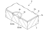
- FIG. 1 is a perspective view of the wiring board 3 with a metal piece according to the embodiment.
- FIG. 2 is an enlarged perspective view showing a wiring board 3 with a metal piece, and is a diagram showing a partial cross section of the wiring board 3 with a metal piece.
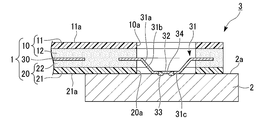
- FIG. 3 is a cross-sectional view of the wiring board 3 with a metal piece.
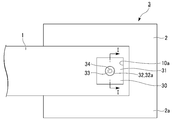
- FIG. 4 is a plan view of the wiring board 3 with a metal piece.
- FIG. 5 is a cross-sectional view taken along the line II of FIG.
- the wiring board 3 with a metal piece includes a flexible printed circuit board (FPC) 1 and a metal piece 2.
- FPC flexible printed circuit board
- the flexible printed circuit board 1 has a first cover ray 10, a second cover ray 20, and a wiring layer 30 (metal layer).
- the flexible printed circuit board 1 has flexibility.
- the flexible printed circuit board 1 is configured so that the wiring layer 30 functions even when it is greatly bent.
- the flexible printed circuit board 1 is an example of a “wiring board”.
- the wiring board is not limited to the flexible printed circuit board, but may be a rigid board.
- the rigid substrate is a wiring substrate including a rigid substrate such as a glass epoxy substrate or a glass substrate, and a wiring layer.
- the thickness direction of the flexible printed circuit board 1 is simply referred to as the thickness direction. Further, the direction from the metal piece 2 toward the flexible printed circuit board 1 along the thickness direction is referred to as an upper direction, and the opposite direction is referred to as a lower direction. Viewing from the top and bottom is called plan view.
- the first coverlay 10 has a first insulator 11 and a first adhesive layer 12 applied to the first insulator 11.
- the second coverlay 20 has a second insulator 21 and a second adhesive layer 22 applied to the second insulator 21.
- the flexible printed circuit board 1 has a laminated structure in which the second cover ray 20, the wiring layer 30, and the first cover ray 10 are laminated in this order from the bottom to the top.
- the first insulator 11 is located on the uppermost layer of the flexible printed circuit board 1
- the second insulator 21 is located on the lowermost layer of the flexible printed circuit board 1.
- the first insulator 11 and the second insulator 21 are formed in a thin film shape.
- flexible and insulating materials can be used.
- the materials of the insulators 11 and 21 include polyimide and liquid crystal polymer.
- a polyimide film having a thickness of 25 ⁇ m is used as the insulators 11 and 21.
- the first adhesive layer 12 adheres the wiring layer 30 and the first insulator 11.
- the second adhesive layer 22 adheres the wiring layer 30 and the second insulator 21.
- a resin having an insulating property and an adhesive property can be used as the material of the adhesive layers 12 and 22.
- the resin having insulating property and adhesiveness include epoxy-based, acrylic-based, and polyimide-based resins.
- an epoxy adhesive having a thickness of 25 ⁇ m is used as the adhesive layers 12 and 22.
- a first opening 10a is formed in the first coverlay 10.
- a second opening 20a (opening) is formed in the second coverlay 20.
- the openings 10a and 20a can be formed by subjecting the coverlays 10 and 20 to laser processing, mold processing, NC processing (Numerical Control machining) and the like.
- the first opening 10a and the second opening 20a are arranged at positions where they overlap each other when viewed from the thickness direction.
- the first opening 10a and the second opening 20a are formed in a square shape.
- the first opening 10a and the second opening 20a have the same shape. The shapes, sizes, arrangements, etc. of the openings 10a and 20a may be changed as appropriate.
- the wiring layer 30 (wiring pattern) is sandwiched between the first cover ray 10 and the second cover ray 20.
- a thin metal film having conductivity can be used.
- the material of the wiring layer 30 include copper, stainless steel, and aluminum.
- the melting point of the material of the wiring layer 30 is preferably higher than the melting point of the material of the metal piece 2.
- an electrolytic copper foil having a thickness of 35 ⁇ m is used as the wiring layer 30.
- the wiring layer 30 can be formed by, for example, a subtractive method, a semi-additive method, or the like.
- the portion of the wiring layer 30 exposed from the first cover lay 10 and the second cover lay 20 through the openings 10a and 20a is referred to as an exposed portion 31.
- a part of the exposed portion 31 is formed in a concave shape downward (that is, toward the metal piece 2).
- the portion deformed in a concave shape toward the metal piece 2 is referred to as a concave deformed portion 31a.
- the concave deformed portion 31a has a reduced diameter portion 31b and a bottom portion 31c.
- the diameter-reduced portion 31b is reduced in diameter downward.
- the cross-sectional shape of the reduced diameter portion 31b orthogonal to the thickness direction is, for example, a circular shape.
- the bottom portion 31c is formed at the lower end of the reduced diameter portion 31b.
- the bottom portion 31c is formed in a disk shape, for example.
- the bottom portion 31c is in contact with the first main surface 2a of the metal piece 2.
- the shape of the concave deformed portion 31a is, for example, a truncated cone shape whose diameter is reduced downward.
- a through hole 32 is formed in the center of the bottom portion 31c.
- the shape of the through hole 32 is a circular shape (see FIGS. 2 and 4).
- the through hole 32 is located at a position overlapping the second opening 20a.
- the inner diameter of the through hole 32 is smaller than the inner diameter of the second opening 20a.
- the through hole 32 is included in the second opening 20a.
- the bottom portion 31c is joined to the metal piece 2 by a welded portion 33 (joining portion) described later.
- the bottom portion 31c is electrically connected to the metal piece 2 by the welded portion 33.
- the electronic component may be a capacitor, a resistor, a thermistor, an IC, an LED, or the like.
- the first coverlay 10 or the second coverlay 20 may be provided with an opening for electrically connecting the electronic component and the wiring layer 30.
- the metal piece 2 is formed of a metal such as aluminum or an aluminum alloy into a plate shape, a film shape, a rod shape, or the like. The material and shape of the metal piece 2 may be changed as appropriate.
- the metal piece 2 may be made of copper, a copper alloy, or the like.
- an aluminum plate (A1050) having a thickness of 1 mm is used as the metal piece 2.
- the upper surface of the metal piece 2 is a first main surface 2a facing the flexible printed circuit board 1.
- the metal piece 2 covers the second opening 20a of the second insulator 21 from below.
- the metal piece 2 is eutectic with a welded portion 33, a non-welded portion 34 (non-joined portion), and a portion facing the wiring layer 30 through the second opening 20a (see FIG. 3). It has a part 35 and the like.
- the welded portion 33 and the non-welded portion 34 are formed in a region including at least the first main surface 2a.
- the welded portion 33 is a portion where the metal piece 2 is melted and then solidified by heating during welding in the joining step described later. That is, the welded portion 33 is a portion having a melting history.
- the welded portion 33 is formed in an annular shape along the peripheral edge portion 32a of the through hole 32 (see FIGS. 2 and 4).
- a part of the welded portion 33 (specifically, the annular outer peripheral portion 33a including the outer peripheral edge of the welded portion 33) is the bottom portion 31c of the wiring layer 30 (specifically, the annular inner peripheral portion 31d including the peripheral edge portion 32a). Located below.
- the inner peripheral portion 31d of the bottom portion 31c covers the outer peripheral portion 33a of the welded portion 33 from above.
- the inner peripheral portion 31d is joined to the outer peripheral portion 33a.
- the welding area between the wiring layer 30 and the metal piece 2 becomes large, and the welding strength can be increased.
- the portion (inner peripheral portion 33b) excluding the outer peripheral portion 33a (the portion overlapping the bottom portion 31c) is inside the through hole 32 in a plan view.
- the inner diameter of the welded portion 33 is smaller than the inner diameter of the through hole 32.
- the welded portion 33 surrounds the non-welded portion 34 on the first main surface 2a (see FIGS. 2 and 4).
- a part of the welded portion 33 bulges upward on the first main surface 2a. This portion is called a bulging portion 33c.
- the bulging portion 33c is an annular portion protruding upward with respect to the surface of the non-welded portion 34.
- the outer peripheral surface of the bulging portion 33c is joined to the inner peripheral surface of the peripheral edge portion 32a.
- the non-welded portion 34 is a portion that has not been melted by heating during welding for joining the wiring layer 30 to the metal piece 2. That is, the non-welded portion 34 is a portion having no melting history.
- the non-welded portion 34 surrounded by the welded portion 33 has a circular shape in a plan view (see FIGS. 2 and 4).
- the eutectic portion 35 is formed at the interface between the bottom portion 31c of the wiring layer 30 and the metal piece 2.
- the eutectic portion 35 is, for example, a portion where the bottom portion 31c and the metal piece 2 are melted and mixed and solidified in a eutectic state.
- the eutectic portion 35 is formed from the inner peripheral surface of the through hole 32 of the bottom portion 31c to the lower surface of the inner peripheral portion 31d.
- the eutectic portion 35 can be said to be an alloy layer (or an intermetallic compound layer) composed of the constituent metal of the wiring layer 30 and the constituent metal of the metal piece 2.
- the shapes of the welded portion 33, the non-welded portion 34, and the eutectic portion 35 are confirmed by observing the cut surfaces of each part of the welded portion 33, the non-welded portion 34, and the eutectic portion 35, X-ray imaging, and the like. be able to.
- FIG. 6 is a photograph of the welded portion 33 of an example of the wiring board 3 with a metal piece seen from above.
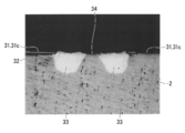
- FIG. 7 is a photograph of a cross section of the welded portion 33. As shown in FIGS. 6 and 7, the welded portion 33 is formed in an annular shape so as to surround the non-welded portion 34.
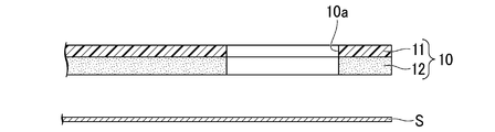
- the preparation step is a step of preparing the flexible printed circuit board 1. As shown in FIG. 8, in the preparation step, the first coverlay 10 and the conductor sheet S are prepared. A first opening 10a is formed in advance in the first coverlay 10. The first adhesive layer 12 of the first coverlay 10 is in a semi-cured state.
- the sheet S is a metal foil made of copper, stainless steel, aluminum, or the like.
- the first coverlay 10 and the seat S are aligned so as to face each other.
- the first coverlay 10 and the sheet S are laminated and integrated by a heating press.
- the first adhesive layer 12 is cured, and the first coverlay 10 and the sheet S are fixed.
- the conditions of the heating press are preferably in the range of, for example, a temperature of 100 to 200 ° C., a pressure of 0.1 to 10 MPa, and a pressurization time of 1 to 120 minutes. If necessary, the first coverlay 10 and the sheet S may be heated in an oven after the heating press.
- the sheet S integrated with the first coverlay 10 is processed to form the wiring layer 30.
- the wiring layer 30 can be obtained by a subtractive method or laser processing.
- the subtractive method is adopted, and the wiring layer 30 is formed by etching the sheet S.
- a through hole 32 is formed in the portion of the wiring layer 30 exposed from the first opening 10a (exposed portion 31).
- the shape of the through hole 32 is a circular shape (see FIG. 2).
- the second coverlay 20 is arranged below the wiring layer 30.
- a second opening 20a is formed in advance in the second coverlay 20.
- the first cover lay 10 and the wiring layer 30 and the second cover lay 20 are positioned and laminated, and integrated by a heating press.
- the second adhesive layer 22 is cured, and the members 10, 20, and 30 are fixed (see FIG. 12).
- the conditions for the heating press may be the same as when the first coverlay 10 and the sheet S are integrated.
- the metal piece 2 is arranged below the integrated first cover ray 10, the wiring layer 30, and the second cover ray 20.
- a part of the exposed portion 31 of the wiring layer 30 and the metal piece 2 are joined (joining step).
- a concave deformed portion 31a is formed in a part of the exposed portion 31.
- a joining method laser welding, resistance welding and the like can be used.
- the laser beam L is emitted downward from the welding laser device 40 to irradiate the exposed portion 31 and the metal piece 2 of the wiring layer 30 (irradiation step).
- the irradiation region of the laser beam L may be, for example, an annular region concentric with the through hole 32 in a plan view.
- the inner diameter of the irradiation region is smaller than the inner diameter of the through hole 32, and the outer diameter of this irradiation region is larger than the inner diameter of the through hole 32.
- the locus (trajectory pattern) of the laser beam L in the irradiation region is not particularly limited, and may be, for example, a wobbling shape, a spiral shape, a plurality of concentric circles, or the like.
- the annular portion of the metal piece 2 along the peripheral edge portion 32a melts and then solidifies.
- the welded portion 33 (see FIG. 5) is formed.
- the portion of the metal piece 2 that has not been melted becomes the non-welded portion 34.
- a part of the bottom portion 31c is joined to the metal piece 2 by the welded portion 33.
- a eutectic portion 35 (see FIG. 5) is formed at the interface between a part of the bottom portion 31c and the metal piece 2.
- the electronic component may be mounted on the flexible printed circuit board 1 before or after joining the wiring layer 30 to the metal piece 2.
- the welded portion 33 for joining the wiring layer 30 to the metal piece 2 is formed in an annular shape along the peripheral edge portion 32a of the through hole 32 so as to surround the non-welded portion 34. .. Since the molten portion of the metal piece 2 during welding is formed in an annular shape and the central portion does not melt, stress concentration is less likely to occur during solidification as compared with the case where the entire circular region is melted. Therefore, it is possible to suppress the occurrence of cracks in the welded portion 33 due to stress concentration during solidification.
- FIG. 18 is a photograph of a cross section of a welded portion 133 of a wiring board with a metal piece in a comparative form.
- the welded portion 133 is formed by melting the entire circular region of the metal piece, not the annular shape.
- a crack C is formed in the welded portion 133 at a position close to the central portion. It can be inferred that this crack C was generated by the concentration of stress in the central portion of the melted portion during solidification.
- the welded portion 33 is formed in an annular shape, it is easy to judge the quality of welding based on the shape of the welded portion 33. Further, as shown in FIG. 5, in the wiring board 3 with a metal piece, the welded portion 33 is formed in contact with the wiring layer 30 in a wide region from the inner peripheral surface of the through hole 32 to the lower surface of the bottom portion 31c. The connection reliability between the layer 30 and the metal piece 2 can be improved.
- the processing time can be shortened.
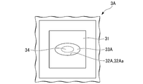
- FIG. 14 is a plan view of a part of the wiring board 3A with a metal piece having the welded portion 33A of the first modification.
- the through hole 32A has an elliptical shape in a plan view.
- the weld 33A is formed in an elliptical ring along the peripheral edge 32Aa of the through hole 32A.
- the welded portion 33A surrounds the non-welded portion 34.
- the elliptical annular welded portion 33A can be appropriately adopted in accordance with the space in which the welded portion is formed in the wiring layer 30 and the metal piece 2.
- FIG. 15 is a plan view of a part of the wiring board 3B with a metal piece having the welded portion 33B of the second modification.
- the through hole 32B is formed in a rectangular shape in a plan view.
- the welded portion 33B is formed in a rectangular ring shape along the peripheral edge portion 32Ba of the through hole 32B.
- the welded portion 33B surrounds the non-welded portion 34.
- the rectangular annular welded portion 33A can be appropriately adopted in accordance with the space in which the welded portion is formed in the wiring layer 30 and the metal piece 2.
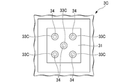
- FIG. 16 is a plan view of a part of the wiring board 3C with a metal piece having the welded portion 33C of the third modification.
- a plurality of welded portions 33C formed in an annular shape are formed similarly to the welded portions 33 shown in FIGS. 1 and 2. Since a plurality of welded portions 33C are formed on the metal piece-attached wiring board 3C, the welding strength can be increased. Since a plurality of welded portions 33C are formed on the wiring board 3C with a metal piece, the electrical resistance of the welded portion can be reduced.
- FIG. 17 is a plan view of a part of the wiring board 3D with a metal piece having the welded portion 33D of the fourth modification.
- a plurality of welded portions 33D are formed in the wiring board 3D with a metal piece.
- the plurality of welded portions 33D include an annular welded portion 33D1 and a rectangular annular welded portion 33D2. Since a plurality of welded portions 33D1 and 33D2 are formed on the wiring board 3D with a metal piece, the welding strength can be increased.
Landscapes
- Engineering & Computer Science (AREA)
- Microelectronics & Electronic Packaging (AREA)
- Physics & Mathematics (AREA)
- Optics & Photonics (AREA)
- Manufacturing & Machinery (AREA)
- Plasma & Fusion (AREA)
- Mechanical Engineering (AREA)
- Structure Of Printed Boards (AREA)
Abstract
Cette carte de câblage ayant une pièce métallique est pourvue : d'une carte de câblage qui a une couche de câblage ayant un trou traversant formé à l'intérieur de celle-ci et d'une couche de couverture ayant une ouverture formée à l'intérieur de celle-ci ; et d'une pièce métallique. Dans une vue en plan, le trou traversant chevauche l'ouverture. La pièce métallique présente, au niveau d'une partie faisant face à la couche de câblage à travers l'ouverture, une section soudée jointe à la couche de câblage, et une section non soudée. La section soudée est formée de façon annulaire de façon à entourer la section non soudée sur la circonférence du trou traversant.
Priority Applications (1)
| Application Number | Priority Date | Filing Date | Title |
|---|---|---|---|
| JP2021562602A JPWO2021111966A1 (fr) | 2019-12-05 | 2020-11-26 |
Applications Claiming Priority (2)
| Application Number | Priority Date | Filing Date | Title |
|---|---|---|---|
| JP2019-220318 | 2019-12-05 | ||
| JP2019220318 | 2019-12-05 |
Publications (1)
| Publication Number | Publication Date |
|---|---|
| WO2021111966A1 true WO2021111966A1 (fr) | 2021-06-10 |
Family
ID=76222373
Family Applications (1)
| Application Number | Title | Priority Date | Filing Date |
|---|---|---|---|
| PCT/JP2020/043952 Ceased WO2021111966A1 (fr) | 2019-12-05 | 2020-11-26 | Carte de câblage ayant une pièce métallique |
Country Status (2)
| Country | Link |
|---|---|
| JP (1) | JPWO2021111966A1 (fr) |
| WO (1) | WO2021111966A1 (fr) |
Cited By (1)
| Publication number | Priority date | Publication date | Assignee | Title |
|---|---|---|---|---|
| JP2025517581A (ja) * | 2022-05-02 | 2025-06-06 | ローベルト ボツシユ ゲゼルシヤフト ミツト ベシユレンクテル ハフツング | 溶接されたフレキシブルなプリント基板を備えたコンタクト構造体 |
Citations (4)
| Publication number | Priority date | Publication date | Assignee | Title |
|---|---|---|---|---|
| JPH0765717A (ja) * | 1993-08-20 | 1995-03-10 | Sony Corp | レーザー溶接方法 |
| JPH11104865A (ja) * | 1997-10-03 | 1999-04-20 | Denso Corp | 溶接構造及び溶接方法 |
| JP2008212993A (ja) * | 2007-03-05 | 2008-09-18 | Toyota Motor Corp | レーザ接合方法 |
| WO2019131828A1 (fr) * | 2017-12-28 | 2019-07-04 | 株式会社フジクラ | Structure de soudage, carte de câblage équipée d'une pièce métallique, et procédé de soudage |
-
2020
- 2020-11-26 WO PCT/JP2020/043952 patent/WO2021111966A1/fr not_active Ceased
- 2020-11-26 JP JP2021562602A patent/JPWO2021111966A1/ja not_active Withdrawn
Patent Citations (4)
| Publication number | Priority date | Publication date | Assignee | Title |
|---|---|---|---|---|
| JPH0765717A (ja) * | 1993-08-20 | 1995-03-10 | Sony Corp | レーザー溶接方法 |
| JPH11104865A (ja) * | 1997-10-03 | 1999-04-20 | Denso Corp | 溶接構造及び溶接方法 |
| JP2008212993A (ja) * | 2007-03-05 | 2008-09-18 | Toyota Motor Corp | レーザ接合方法 |
| WO2019131828A1 (fr) * | 2017-12-28 | 2019-07-04 | 株式会社フジクラ | Structure de soudage, carte de câblage équipée d'une pièce métallique, et procédé de soudage |
Cited By (1)
| Publication number | Priority date | Publication date | Assignee | Title |
|---|---|---|---|---|
| JP2025517581A (ja) * | 2022-05-02 | 2025-06-06 | ローベルト ボツシユ ゲゼルシヤフト ミツト ベシユレンクテル ハフツング | 溶接されたフレキシブルなプリント基板を備えたコンタクト構造体 |
Also Published As
| Publication number | Publication date |
|---|---|
| JPWO2021111966A1 (fr) | 2021-06-10 |
Similar Documents
| Publication | Publication Date | Title |
|---|---|---|
| US11597038B2 (en) | Welding structure, wiring board with metal piece, and welding method | |
| JP4902606B2 (ja) | 半導体パッケージの製造方法及びそれを用いた半導体プラスチックパッケージ | |
| CN1174665C (zh) | 多层挠性布线板 | |
| JP4554873B2 (ja) | 配線板、電子機器および電子部品の実装方法並びに製造方法 | |
| US9713267B2 (en) | Method for manufacturing printed wiring board with conductive post and printed wiring board with conductive post | |
| WO2012111711A1 (fr) | Substrat câblé multicouche, et procédé de production associé | |
| JPWO2007034629A1 (ja) | 部品内蔵モジュールの製造方法および部品内蔵モジュール | |
| JP5688162B2 (ja) | 部品内蔵基板の製造方法及びこの方法を用いて製造した部品内蔵基板 | |
| WO2021111966A1 (fr) | Carte de câblage ayant une pièce métallique | |
| JP6930661B2 (ja) | 基板接合構造 | |
| JPWO2020122166A1 (ja) | シールドプリント配線板及びシールドプリント配線板の製造方法 | |
| JPWO2012161218A1 (ja) | 配線板および配線板の製造方法 | |
| JPH07231165A (ja) | 多層配線基板及びその製造方法 | |
| JP5175694B2 (ja) | 多層板の製造方法および多層プリント配線板の製造方法 | |
| JP4856567B2 (ja) | プリント配線板及び電子部品実装基板 | |
| JP2007088058A (ja) | 多層基板、及びその製造方法 | |
| JP5515210B2 (ja) | 部品内蔵配線板、部品内蔵配線板の製造方法 | |
| JP2020155537A (ja) | 金属片付き配線基板 | |
| JP2019216228A (ja) | 金属片付き配線基板および金属片付き配線基板の製造方法 | |
| WO2017061369A1 (fr) | Substrat de résine et procédé de fabrication de substrat de résine | |
| CN118945991A (zh) | 印制线路板及其制作方法、电子设备 | |
| JP6287538B2 (ja) | 多層基板、及びその製造方法 | |
| JP2020155548A (ja) | 金属片付き配線基板および金属片付き配線基板の製造方法 | |
| JP2022114983A (ja) | チップ抵抗器及びチップ抵抗器の製造方法 | |
| JPH01232794A (ja) | はんだ付け方法 |
Legal Events
| Date | Code | Title | Description |
|---|---|---|---|
| 121 | Ep: the epo has been informed by wipo that ep was designated in this application |
Ref document number: 20896479 Country of ref document: EP Kind code of ref document: A1 |
|
| ENP | Entry into the national phase |
Ref document number: 2021562602 Country of ref document: JP Kind code of ref document: A |
|
| NENP | Non-entry into the national phase |
Ref country code: DE |
|
| 122 | Ep: pct application non-entry in european phase |
Ref document number: 20896479 Country of ref document: EP Kind code of ref document: A1 |