WO2022244745A1 - 基板処理方法 - Google Patents
基板処理方法 Download PDFInfo
- Publication number
- WO2022244745A1 WO2022244745A1 PCT/JP2022/020422 JP2022020422W WO2022244745A1 WO 2022244745 A1 WO2022244745 A1 WO 2022244745A1 JP 2022020422 W JP2022020422 W JP 2022020422W WO 2022244745 A1 WO2022244745 A1 WO 2022244745A1
- Authority
- WO
- WIPO (PCT)
- Prior art keywords
- substrate
- processing
- substrates
- batch
- processing unit
- Prior art date
- Legal status (The legal status is an assumption and is not a legal conclusion. Google has not performed a legal analysis and makes no representation as to the accuracy of the status listed.)
- Ceased
Links
Images



Classifications
-
- H—ELECTRICITY
- H10—SEMICONDUCTOR DEVICES; ELECTRIC SOLID-STATE DEVICES NOT OTHERWISE PROVIDED FOR
- H10P—GENERIC PROCESSES OR APPARATUS FOR THE MANUFACTURE OR TREATMENT OF DEVICES COVERED BY CLASS H10
- H10P72/00—Handling or holding of wafers, substrates or devices during manufacture or treatment thereof
- H10P72/04—Apparatus for manufacture or treatment
- H10P72/0402—Apparatus for fluid treatment
- H10P72/0404—Apparatus for fluid treatment for general liquid treatment, e.g. etching followed by cleaning
-
- H—ELECTRICITY
- H10—SEMICONDUCTOR DEVICES; ELECTRIC SOLID-STATE DEVICES NOT OTHERWISE PROVIDED FOR
- H10P—GENERIC PROCESSES OR APPARATUS FOR THE MANUFACTURE OR TREATMENT OF DEVICES COVERED BY CLASS H10
- H10P50/00—Etching of wafers, substrates or parts of devices
- H10P50/60—Wet etching
- H10P50/64—Wet etching of semiconductor materials
- H10P50/642—Chemical etching
-
- H—ELECTRICITY
- H10—SEMICONDUCTOR DEVICES; ELECTRIC SOLID-STATE DEVICES NOT OTHERWISE PROVIDED FOR
- H10P—GENERIC PROCESSES OR APPARATUS FOR THE MANUFACTURE OR TREATMENT OF DEVICES COVERED BY CLASS H10
- H10P50/00—Etching of wafers, substrates or parts of devices
-
- H—ELECTRICITY
- H10—SEMICONDUCTOR DEVICES; ELECTRIC SOLID-STATE DEVICES NOT OTHERWISE PROVIDED FOR
- H10P—GENERIC PROCESSES OR APPARATUS FOR THE MANUFACTURE OR TREATMENT OF DEVICES COVERED BY CLASS H10
- H10P52/00—Grinding, lapping or polishing of wafers, substrates or parts of devices
-
- H—ELECTRICITY
- H10—SEMICONDUCTOR DEVICES; ELECTRIC SOLID-STATE DEVICES NOT OTHERWISE PROVIDED FOR
- H10P—GENERIC PROCESSES OR APPARATUS FOR THE MANUFACTURE OR TREATMENT OF DEVICES COVERED BY CLASS H10
- H10P72/00—Handling or holding of wafers, substrates or devices during manufacture or treatment thereof
- H10P72/04—Apparatus for manufacture or treatment
- H10P72/0402—Apparatus for fluid treatment
- H10P72/0406—Apparatus for fluid treatment for cleaning followed by drying, rinsing, stripping, blasting or the like
-
- H—ELECTRICITY
- H10—SEMICONDUCTOR DEVICES; ELECTRIC SOLID-STATE DEVICES NOT OTHERWISE PROVIDED FOR
- H10P—GENERIC PROCESSES OR APPARATUS FOR THE MANUFACTURE OR TREATMENT OF DEVICES COVERED BY CLASS H10
- H10P72/00—Handling or holding of wafers, substrates or devices during manufacture or treatment thereof
- H10P72/04—Apparatus for manufacture or treatment
- H10P72/0402—Apparatus for fluid treatment
- H10P72/0406—Apparatus for fluid treatment for cleaning followed by drying, rinsing, stripping, blasting or the like
- H10P72/0408—Apparatus for fluid treatment for cleaning followed by drying, rinsing, stripping, blasting or the like for drying
-
- H—ELECTRICITY
- H10—SEMICONDUCTOR DEVICES; ELECTRIC SOLID-STATE DEVICES NOT OTHERWISE PROVIDED FOR
- H10P—GENERIC PROCESSES OR APPARATUS FOR THE MANUFACTURE OR TREATMENT OF DEVICES COVERED BY CLASS H10
- H10P72/00—Handling or holding of wafers, substrates or devices during manufacture or treatment thereof
- H10P72/04—Apparatus for manufacture or treatment
- H10P72/0402—Apparatus for fluid treatment
- H10P72/0406—Apparatus for fluid treatment for cleaning followed by drying, rinsing, stripping, blasting or the like
- H10P72/0411—Apparatus for fluid treatment for cleaning followed by drying, rinsing, stripping, blasting or the like for wet cleaning or washing
-
- H—ELECTRICITY
- H10—SEMICONDUCTOR DEVICES; ELECTRIC SOLID-STATE DEVICES NOT OTHERWISE PROVIDED FOR
- H10P—GENERIC PROCESSES OR APPARATUS FOR THE MANUFACTURE OR TREATMENT OF DEVICES COVERED BY CLASS H10
- H10P72/00—Handling or holding of wafers, substrates or devices during manufacture or treatment thereof
- H10P72/04—Apparatus for manufacture or treatment
- H10P72/0402—Apparatus for fluid treatment
- H10P72/0418—Apparatus for fluid treatment for etching
- H10P72/0422—Apparatus for fluid treatment for etching for wet etching
- H10P72/0424—Apparatus for fluid treatment for etching for wet etching using mainly spraying means, e.g. nozzles
-
- H—ELECTRICITY
- H10—SEMICONDUCTOR DEVICES; ELECTRIC SOLID-STATE DEVICES NOT OTHERWISE PROVIDED FOR
- H10P—GENERIC PROCESSES OR APPARATUS FOR THE MANUFACTURE OR TREATMENT OF DEVICES COVERED BY CLASS H10
- H10P72/00—Handling or holding of wafers, substrates or devices during manufacture or treatment thereof
- H10P72/04—Apparatus for manufacture or treatment
- H10P72/0451—Apparatus for manufacturing or treating in a plurality of work-stations
- H10P72/0452—Apparatus for manufacturing or treating in a plurality of work-stations characterised by the layout of the process chambers
- H10P72/0454—Apparatus for manufacturing or treating in a plurality of work-stations characterised by the layout of the process chambers surrounding a central transfer chamber
-
- H—ELECTRICITY
- H10—SEMICONDUCTOR DEVICES; ELECTRIC SOLID-STATE DEVICES NOT OTHERWISE PROVIDED FOR
- H10P—GENERIC PROCESSES OR APPARATUS FOR THE MANUFACTURE OR TREATMENT OF DEVICES COVERED BY CLASS H10
- H10P72/00—Handling or holding of wafers, substrates or devices during manufacture or treatment thereof
- H10P72/04—Apparatus for manufacture or treatment
- H10P72/0451—Apparatus for manufacturing or treating in a plurality of work-stations
- H10P72/0461—Apparatus for manufacturing or treating in a plurality of work-stations characterised by the presence of two or more transfer chambers
-
- H—ELECTRICITY
- H10—SEMICONDUCTOR DEVICES; ELECTRIC SOLID-STATE DEVICES NOT OTHERWISE PROVIDED FOR
- H10P—GENERIC PROCESSES OR APPARATUS FOR THE MANUFACTURE OR TREATMENT OF DEVICES COVERED BY CLASS H10
- H10P72/00—Handling or holding of wafers, substrates or devices during manufacture or treatment thereof
- H10P72/06—Apparatus for monitoring, sorting, marking, testing or measuring
-
- H—ELECTRICITY
- H10—SEMICONDUCTOR DEVICES; ELECTRIC SOLID-STATE DEVICES NOT OTHERWISE PROVIDED FOR
- H10P—GENERIC PROCESSES OR APPARATUS FOR THE MANUFACTURE OR TREATMENT OF DEVICES COVERED BY CLASS H10
- H10P72/00—Handling or holding of wafers, substrates or devices during manufacture or treatment thereof
- H10P72/30—Handling or holding of wafers, substrates or devices during manufacture or treatment thereof for conveying, e.g. between different workstations
- H10P72/32—Handling or holding of wafers, substrates or devices during manufacture or treatment thereof for conveying, e.g. between different workstations between different workstations
-
- H—ELECTRICITY
- H10—SEMICONDUCTOR DEVICES; ELECTRIC SOLID-STATE DEVICES NOT OTHERWISE PROVIDED FOR
- H10P—GENERIC PROCESSES OR APPARATUS FOR THE MANUFACTURE OR TREATMENT OF DEVICES COVERED BY CLASS H10
- H10P72/00—Handling or holding of wafers, substrates or devices during manufacture or treatment thereof
- H10P72/30—Handling or holding of wafers, substrates or devices during manufacture or treatment thereof for conveying, e.g. between different workstations
- H10P72/34—Handling or holding of wafers, substrates or devices during manufacture or treatment thereof for conveying, e.g. between different workstations the wafers being stored in a carrier, involving loading and unloading
-
- H—ELECTRICITY
- H10—SEMICONDUCTOR DEVICES; ELECTRIC SOLID-STATE DEVICES NOT OTHERWISE PROVIDED FOR
- H10P—GENERIC PROCESSES OR APPARATUS FOR THE MANUFACTURE OR TREATMENT OF DEVICES COVERED BY CLASS H10
- H10P72/00—Handling or holding of wafers, substrates or devices during manufacture or treatment thereof
- H10P72/30—Handling or holding of wafers, substrates or devices during manufacture or treatment thereof for conveying, e.g. between different workstations
- H10P72/34—Handling or holding of wafers, substrates or devices during manufacture or treatment thereof for conveying, e.g. between different workstations the wafers being stored in a carrier, involving loading and unloading
- H10P72/3411—Handling or holding of wafers, substrates or devices during manufacture or treatment thereof for conveying, e.g. between different workstations the wafers being stored in a carrier, involving loading and unloading involving loading and unloading of wafers
- H10P72/3412—Batch transfer of wafers
Definitions
- substrates to be processed include, for example, semiconductor wafers, glass substrates for liquid crystal display devices, flat panel display (FPD) substrates such as organic EL (electroluminescence) display devices, optical disk substrates, magnetic disk substrates, It includes a magneto-optical disk substrate, a photomask glass substrate, a ceramic substrate, a field emission display (FED) substrate, a solar cell substrate, and the like.
- FPD flat panel display
- FED field emission display
- a batch-type processing apparatus (hereinafter also referred to as a batch processing unit) that uses phosphoric acid to etch a silicon nitride film on a substrate (see Patent Document 1, for example).
- a batch processing apparatus can process a plurality of substrates at once, and thus has a high throughput.
- a single-wafer processing apparatus that processes substrates one by one (hereinafter also referred to as a single-wafer processing unit) has a high drying capacity, so the above drying process can be performed appropriately.
- the technology disclosed in the specification of the present application has been made in view of the problems described above, and is capable of efficiently advancing the overall substrate processing in substrate processing using a batch processing unit and a single substrate processing unit. It is a technology for
- a substrate processing method which is a first aspect of the technology disclosed in the specification of the present application, includes a batch processing unit that performs substrate processing including chemical liquid processing on a plurality of substrates, and the substrate processing including drying processing on one substrate. and at least one single-wafer processing unit performing the drying process in the single-wafer processing unit after the chemical solution processing is performed in the batch processing unit. a step of calculating a required time, which is the time required for the substrates to finish the substrate processing in the single-wafer processing unit, according to the number of waiting substrates, which is the number of the substrates before performing the required time; and controlling the start time of the chemical processing in the batch processing section so as to be shorter than the time required for the chemical processing in the batch processing section.
- a substrate processing method that is a second aspect of the technology disclosed in this specification relates to the substrate processing method that is the first aspect, and the required time includes the remaining time of the ongoing substrate processing. .
- a substrate processing method which is a third aspect of the technology disclosed in the specification of the present application, comprises a batch processing unit that performs substrate processing including chemical liquid processing on a plurality of substrates, and the substrate processing including drying processing on one substrate. and at least one single-wafer processing unit performing the drying process in the single-wafer processing unit after the chemical solution processing is performed in the batch processing unit. a step of calculating a required time, which is the time required for the substrates to finish the substrate processing in the single-wafer processing unit, according to the number of waiting substrates, which is the number of the substrates before performing the required time; and changing the number of substrates to be processed in the batch processing section so as to be shorter than the time required for the chemical liquid processing in the batch processing section.
- a substrate processing method relates to the substrate processing method according to any one of the first to third aspects, wherein the chemical solution processing is performed in the batch processing section.
- a substrate processing method relates to the substrate processing method according to any one of the first to third aspects, wherein in the single-wafer processing unit, the drying The method further comprises performing a cleaning process on the substrate before processing is performed.
- a substrate processing method that is a sixth aspect of the technology disclosed in the specification of the present application relates to the substrate processing method that is a fifth aspect, and the step of calculating the required time includes: It is a step of calculating the required time including the time required for the cleaning process according to the number of waiting substrates before moving to the processing section.
- a substrate processing method relates to the substrate processing method according to any one of the first to sixth aspects, wherein the chemical solution processing in the batch processing section includes , the substrate is immersed in a chemical tank, and in the batch processing unit, the plurality of substrates after the chemical treatment is immersed in a cleaning tank to perform a cleaning process;
- the bath has a first area where the chemical treatment is started at a first start time and a second area where the chemical treatment is started at a second start time different from the first start time.
- the cleaning tank includes a third area for performing the cleaning process on the substrate that has been subjected to the chemical treatment in the first area, and a third area that has been subjected to the chemical treatment in the second area. and a fourth region for performing the cleaning process on the substrate.
- a substrate processing method relates to the substrate processing method according to any one of the first to seventh aspects, wherein the required time is a It includes the time it takes to move from the batch processing unit to the single wafer processing unit.
- a substrate processing method relates to the substrate processing method according to any one of the first to eighth aspects, wherein the required time is includes the time required for attitude change for the substrate processed in the above to be processed in the single-wafer processing unit.
- a substrate processing method relates to the substrate processing method according to any one of the first to ninth aspects, wherein the required time is the number of standby sheets. It includes the time required for the substrate processing performed repeatedly in one single wafer processing unit when the substrates are distributed to a plurality of the single wafer processing units.
- substrates waiting until drying processing is performed in the single-wafer processing unit after chemical processing is performed in the batch processing unit.
- An increase in the number of sheets can be suppressed. Therefore, the entire substrate processing performed by the batch processing section and the single wafer processing section can be efficiently advanced.
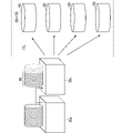
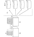
- FIG. 2 is a diagram partially and schematically showing an example of a three-dimensional structure formed on a substrate; 4 is a flow chart that schematically illustrates an example of a process for treating a substrate, according to an embodiment. It is a figure which shows roughly an example of a structure of a batch processing part. It is a figure which shows roughly an example of a structure of a conveyance robot. It is a figure which shows roughly an example of a structure of a conveyance robot. It is a figure which shows roughly an example of a structure of a single wafer processing part.
- FIG. 1 is a diagram schematically showing an example of the configuration of a transport robot and its surroundings;
- FIG. 1 is a conceptual diagram schematically showing the relationship of formula (1);
- FIG. 1 is a conceptual diagram schematically showing the relationship of formula (2);
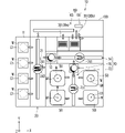
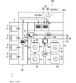
- BRIEF DESCRIPTION OF THE DRAWINGS It is a top view which shows roughly an example of a structure of a substrate processing apparatus regarding embodiment.
- FIG. 3 is a conceptual diagram schematically showing the relationship of formula (3);
- FIG. 4 is a conceptual diagram schematically showing the relationship of formula (4);
- FIG. 1 is a plan view schematically showing an example of the configuration of a substrate processing apparatus 10 according to this embodiment.
- the Z-axis direction is the vertically upward direction.
- the substrate processing apparatus 10 is an apparatus that performs wet processing on the substrate W. As shown in FIG. 1
- the substrate W is, for example, a semiconductor substrate, and a surface pattern is formed on its surface.
- a specific example of the surface pattern is a three-dimensional structure formed during the manufacture of a three-dimensional NAND (Not-AND) flash memory.
- FIG. 2 is a diagram partially and schematically showing an example of a three-dimensional structure formed on the substrate W.
- substrate W includes support layer 93 .
- Support layer 93 is, for example, a silicon layer.
- a laminated structure 90 is formed on the upper surface of the support layer 93 .
- a laminated structure 90 includes a plurality of insulating films 91 and a plurality of sacrificial films 92 .
- the insulating films 91 and the sacrificial films 92 are alternately laminated in the Z-axis direction.
- Insulating film 91 is, for example, a silicon dioxide film
- sacrificial film 92 is, for example, a silicon nitride film.
- Insulating film 91 and sacrificial film 92 have a thickness of, for example, 1 nm or more and 50 nm or less.
- a trench 94 is also formed in the laminated structure 90 .
- the trench 94 penetrates the laminate structure 90 along the thickness direction of the substrate W.
- the laminated structure 90 is provided with pillars (not shown).
- the pillar supports the insulating film 91 when the sacrificial film 92 is removed.
- the width of the pillar (the width parallel to the main surface of the substrate W) is, for example, 1 nm or more and 50 nm or less.
- the substrate processing apparatus 10 may perform other processes on the substrate W as well.
- An example of the overall configuration of the substrate processing apparatus 10 will be outlined below, and then an example of each configuration will be described in detail.
- the substrate processing apparatus 10 includes a batch processing section 30 that collectively processes a plurality of substrates W (that is, performs batch-type substrate processing), A single-wafer processing unit 50 that processes the substrates one by one (that is, performs single-wafer type substrate processing), an inter-batch transfer unit 60, and an inter-batch transfer unit 70 are provided.
- the substrate processing apparatus 10 includes a housing 100, and the housing 100 includes at least the batch processing section 30, the single wafer processing section 50, the inter-batch transfer section 60, and the batch processing section 60.
- the sheet-to-sheet transfer unit 70 is accommodated. That is, in the example of FIG. 1, the substrate processing apparatus 10 is a hybrid type substrate processing apparatus in which the batch processing section 30 and the single-wafer processing section 50 coexist within the same housing 100 .
- the substrate processing apparatus 10 is also provided with a load port 11 as a loading port into which a plurality of substrates W are loaded from the outside.
- a portable container (hereinafter referred to as a carrier C1) that stores a plurality of substrates W is loaded into the load port 11 .
- a plurality of carriers C1 are placed in a row along the Y-axis direction in the load port 11 .
- a FOUP Front Opening Unified Pod
- a SMIF Standard Mechanical InterFace
- an OC Open Cassette
- a plurality of substrates W are accommodated in the carrier C1 in a horizontal posture in which the surface thereof faces the positive Z-axis direction and are arranged side by side in the Z-axis direction.
- the horizontal posture referred to here is a posture in which the thickness direction of the substrate W is along the Z-axis direction.
- the number of substrates W stored in the carrier C1 is not particularly limited, it is, for example, 25 substrates.
- the substrate processing apparatus 10 is also provided with an indexer transport section 20 that transports a plurality of substrates W between each carrier C1 and the inter-batch transport section 60 .
- the indexer transport section 20 is provided inside the housing 100 .
- the indexer transport section 20 collectively takes out a plurality of substrates W from each carrier C1, converts the posture of the substrates W from the horizontal posture to the standing posture, and transports the plurality of substrates W in the standing posture to the inter-batch transport section 60. do.
- the standing posture referred to here is a posture in which the thickness direction of the substrate W is along the horizontal direction.
- the indexer transport section 20 transfers a plurality of substrates W to the inter-batch transport section 60, for example, in an upright posture in which the surfaces of the substrates W face the Y-axis negative direction.
- the inter-batch transport section 60 collectively receives a plurality of substrates W in the standing posture from the indexer transport section 20 and sequentially transports the received multiple substrates W collectively to the batch processing section 30 .
- the batch processing unit 30 is a batch-type processing apparatus that performs wet processing on a plurality of substrates W at once.
- the batch processing section 30 includes a processing tank 31, which will be described later.
- a processing liquid is stored in the processing tank 31 .
- the batch processing section 30 can collectively perform processing on the plurality of substrates W according to the processing liquid.
- a plurality of batch processing units 30 are arranged in a row along the X-axis direction.
- a batch processing unit 30a for chemical solution and a batch processing unit 30b for rinse solution are provided as the plurality of batch processing units 30.
- the processing tank 31 of the batch processing section 30a stores the chemical solution.
- the chemical contains an etchant (for example, high-temperature phosphoric acid) capable of removing the sacrificial film 92 .
- an etchant for example, high-temperature phosphoric acid
- the chemical solution acts on the sacrificial film 92 through the trenches 94 of the respective substrates W, and the sacrificial film 92 can be etched.
- the processing tank 31 of the batch processing section 30b stores the rinse liquid.
- the rinse liquid contains pure water, for example.
- the inter-batch transport section 60 first receives the plurality of substrates W in the standing posture from the indexer transport section 20, and transports the received plurality of substrates W to the batch processing section 30a.
- the plurality of substrates W are collectively processed with a chemical solution by the batch processing section 30a. This removes the sacrificial film 92 of each substrate W, for example. By removing the sacrificial film 92 , the insulating film 91 is no longer supported by the sacrificial film 92 . Therefore, insulating film 91 is likely to collapse.
- the inter-batch transfer section 60 receives the plurality of chemically treated substrates W from the batch processing section 30a and transfers the received plurality of substrates W to the batch processing section 30b.
- the plurality of substrates W are transported with the processing liquid (here, the chemical liquid) adhered thereto. Therefore, during this transport, it is possible to suppress the collapse of the three-dimensional structure (for example, the insulating film 91) of the substrate W due to drying.
- a plurality of substrates W transported to the batch processing section 30b are collectively rinsed by the batch processing section 30b.
- the chemical liquid adhering to each substrate W is replaced with the rinse liquid.
- the batch sheet-to-sheet transfer section 70 is provided in the Y-axis negative direction with respect to the batch processing section 30b.
- the batch-to-single-wafer transfer unit 70 receives a plurality of substrates W taken out from the batch processing unit 30b by the batch-to-batch transfer unit 60, and transfers each substrate W to the single-wafer processing unit 50 one by one.
- the inter-batch transfer section 70 takes out the substrate W to which the rinse liquid is attached from the inter-batch transfer section 60 . Then, the batch inter-wafer transfer unit 70 transfers each substrate W in the horizontal posture to the single-wafer processing unit 50 one by one.
- the single-wafer processing unit 50 is provided in the Y-axis negative direction with respect to the batch inter-wafer transfer unit 70 .
- a plurality of single-wafer processing units 50 are arranged in a matrix in plan view.
- four single-wafer processing units 50 are arranged in a matrix of 2 rows and 2 columns.
- the batch inter-wafer transfer unit 70 transfers the substrate W one by one to each of the single-wafer processing units 50 .
- the single-wafer processing unit 50 performs at least a drying process on the substrate W.
- the drying treatment is not particularly limited, it may be, for example, spin drying. That is, the single-wafer processing section 50 may dry the substrate W by rotating the substrate W around a rotation axis Q1 passing through the center of the substrate W and along the Z-axis. Since the single substrate processing unit 50 dries the substrates W one by one, the substrates W can be dried with higher drying performance. Therefore, collapse of the three-dimensional structure of the substrate W due to drying can be suppressed.
- the single-wafer processing unit 50 may appropriately supply a rinse liquid (pure water), IPA, or the like to the main surface of the substrate W as a process prior to the drying process.
- a rinse liquid pure water
- IPA IPA
- the batch inter-wafer transfer section 70 takes out the dried substrate W from each single wafer processing section 50 and transfers the substrate W to the indexer transfer section 20 through the relay unit 12 .
- the relay unit 12 includes a storage container (not shown) that stores a plurality of substrates W arranged in the Z-axis direction.
- the batch inter-wafer transfer unit 70 transfers the substrates W from the single-wafer processing unit 50 to the relay unit 12 one by one.
- the number of substrates W stored in the relay unit 12 increases each time the substrates are transported.
- the indexer transport section 20 collectively takes out the plurality of substrates W from the relay unit 12 and loads the plurality of substrates W onto the load port 11 . Transport to carrier C1.
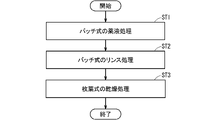
- FIG. 3 is a flowchart schematically showing an example of processing steps for a substrate W according to this embodiment. As an example is shown in FIG. 3, first, a plurality of substrates W are subjected to batch-type chemical treatment (step ST1).
- the rinse treatment may be a single-wafer rinse treatment.
- each substrate W is subjected to a single-wafer drying process (step ST3).
- the substrate W dried by the single wafer processing unit 50 is transported to the carrier C1 via the batch inter-wafer transport unit 70, the relay unit 12 and the indexer transport unit 20.
- the batch processing section 30 can collectively process a plurality of substrates W (steps ST1 and ST2). Thereby, substrates W can be processed with high throughput.
- the substrates W are subjected to a drying process one by one by the single wafer processing unit 50 (step ST3). That is, in the present embodiment, after the batch type wet processing, the single wafer type dry processing is performed instead of the batch type. Therefore, the substrate W can be dried with high drying performance. Therefore, collapse of the three-dimensional structure of the substrate W due to drying can be suppressed.
- the indexer transport section 20 includes a transport robot 21 .
- the transfer robot 21 is provided so as to be movable along the Y-axis direction in the positive direction of the X-axis relative to the load port 11 .
- the transport robot 21 can stop at a position facing each carrier C1 placed on the load port 11 in the X-axis direction.
- the transport robot 21 includes a plurality of (for example, 25) hands 211 and upright support members 212 .
- a plurality of hands 211 are provided side by side in the Z-axis direction.
- the transport robot 21 moves a plurality of hands 211 to take out a plurality of unprocessed substrates W from the carrier C1. Thereby, one substrate W is placed on each hand 211 .
- Each hand 211 is provided with an upright support member 212 that supports the substrate W at its base.
- the upright support member 212 is provided movably in the X-axis direction, and moves in the X-axis negative direction while the substrate W is held on the hand 211 to move the end of the substrate W in the X-axis negative direction.
- the part is sandwiched in its thickness direction.
- the transport robot 21 has a posture conversion function that changes the posture of a plurality of substrates W from a horizontal posture to an upright posture. Specifically, the transport robot 21 rotates the hands 211 by 90 degrees around the rotation axis along the Y-axis direction. This rotation is realized, for example, by a motor or the like. Thereby, the thickness direction of the substrate W is along the X-axis direction. Also, the transport robot 21 rotates the plurality of hands 211 by 90 degrees around the rotation axis along the Z-axis direction. This rotation is also realized, for example, by a motor or the like. Thereby, the thickness direction of the substrate W is along the Y-axis direction.
- the transport robot 21 changes the posture of the substrate W so that the surface of the substrate W faces the Y-axis negative direction. Then, while holding the plurality of substrates W, the transfer robot 21 moves to the end of the movement path in the positive Y-axis direction, and transfers the plurality of substrates W to the inter-batch transfer section 60 .
- the indexer transport section 20 takes out a plurality of unprocessed substrates W from the carrier C1, converts the posture of the substrates W to the standing posture, and transports the plurality of substrates W in the standing posture to the inter-batch transport section 60. .
- the transport robot 21 collectively takes out a plurality of processed substrates W from the relay unit 12 at a predetermined position on the movement path. Then, the transport robot 21 stores the plurality of processed substrates W in the carrier C1 of the load port 11 .
- the batch processing section 30 will be described.
- the batch processing units 30 are arranged in a line along the X-axis direction.
- FIG. 4 is a diagram schematically showing an example of the configuration of the batch processing section 30.
- the batch processing section 30 includes a processing tank 31 and a lifter 32 .
- the processing bath 31 has a box shape that opens in the positive direction of the Z-axis, and stores the processing liquid.
- the lifter 32 includes a plurality of (three in the drawing) holding members 33 that hold a plurality of substrates W in an upright posture, a base 34 that supports the holding members 33, and an elevating mechanism 35 that raises and lowers the base 34.
- Each holding member 33 has an elongated shape extending in the Y-axis direction, and its base end in the positive Y-axis direction is attached to the base 34 .
- a plurality of grooves (not shown) are formed side by side in the Y-axis direction in each holding member 33 . The pitch of the grooves is equal to the pitch of the plurality of substrates W. As shown in FIG.
- the base 34 has a plate-like shape and is provided in a posture in which its thickness direction is along the Y-axis direction.
- the elevating mechanism 35 elevates the plurality of substrates W held by the holding member 33 by elevating the base 34 .
- the lifter 32 is sometimes described as the subject of elevation by the elevation mechanism 35 .
- the lifter 32 raises and lowers the plurality of substrates W between the transfer position in the Z-axis positive direction from the processing tank 31 and the processing position within the processing tank 31 .
- the transfer position is a position at which a plurality of substrates are transferred between the lifter 32 and the inter-batch transfer section 60 .
- the lifter 32 positioned at the delivery position is indicated by solid lines.
- a processing position is a position where a plurality of substrates W are immersed in the processing liquid.
- a plurality of substrates W are processed by the lifter 32 moving the plurality of substrates W to the processing position.
- the lifter 32 and the substrate W positioned at the processing position are schematically indicated by two-dot chain lines.
- the number of substrates W to be processed in the processing bath 31 is not limited to the number of substrates W corresponding to the total capacity of the processing bath 31. It may be the number of substrates W corresponding to half of the total possible capacity.
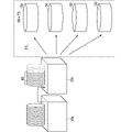
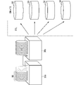
- the processing bath 31 may be divided into a plurality of regions, and substrate processing (including chemical processing and rinsing processing) may be performed at different start timings in each region.
- substrate processing including chemical processing and rinsing processing
- two areas are provided in the processing tank 31 of the batch processing section 30a in FIG. can be rinsed.
- the batch processing section 30 is provided with a supply section for supplying the processing liquid to the processing tank 31 and a discharge section for discharging the processing liquid from the processing tank 31 .
- a gas supply unit that supplies gas to the processing liquid in the processing tank 31 and a circulation unit that returns the processing liquid overflowing from the positive Z-axis direction of the processing tank 31 to the processing tank 31 again. Either one may be provided in the batch processing section 30 .
- the inter-batch transport section 60 includes a transport robot 65 and a transport robot 66 .
- the transfer robot 65 of the inter-batch transfer section 60 includes a pair of holding members 611 and an opening/closing mechanism 613 .
- the holding member 611 is a member that holds a plurality of substrates W in an upright posture.
- the holding members 611 are arranged side by side in the X-axis direction and attached to a base member (not shown) so as to be displaceable.
- the opening/closing mechanism 613 displaces the holding member 611 between the closed position and the open position.
- the closed position is a position where the distance between the two holding members 611 is narrow and where the holding members 611 sandwich a plurality of substrates W.
- FIG. In the example of FIG. 4, the holding member 611 positioned at the closed position is schematically indicated by a chain double-dashed line.
- the open position is a position where the space between the two holding members 611 is wider than the space between the two holding members 611 at the closed position, and is a position where the holding members 611 release the plurality of substrates W held.
- the opening/closing mechanism 613 has, for example, a motor or an air cylinder.
- the transport robot 65 is provided movably in the X-axis direction directly above the batch processing units 30a and 30b.
- a movement mechanism for example, a ball screw mechanism
- the transport robot 65 receives a plurality of substrates W in the upright posture from the indexer transport section 20 (for example, the transport robot 21) at the end in the negative direction of the X-axis in its movement path.
- the transport robot 65 receives a plurality of substrates W in an upright posture in which the surface of the substrate W faces the positive Y-axis direction. Then, the transport robot 65 transports the plurality of substrates W to the batch processing section 30a and the batch processing section 30b in this order.
- the transport robot 66 is provided movably along the X-axis direction right above the batch processing section 30b.
- the transport robot 66 receives a plurality of substrates W in the standing posture from the batch processing section 30 b and transports the plurality of substrates W to the batch inter-wafer transport section 70 .
- the transport robot 66 receives a plurality of substrates W in the standing posture from the batch processing section 30b, and converts the posture of the plurality of substrates W from the standing posture to the horizontal posture.
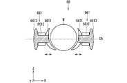
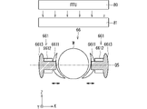
- FIG. 5 and 6 are diagrams schematically showing an example of the configuration of the transport robot 66.
- FIG. 5 shows the transfer robot 66 as viewed along the Y-axis direction
- FIG. 6 shows the transfer robot 66 as viewed along the Z-axis direction.
- the transport robot 66 includes a pair of holding members 661, a base 662, an opening/closing mechanism 663, and a rotating mechanism 664.
- the holding member 661 is a member that holds a plurality of substrates W. As shown in FIG.
- the holding member 661 includes a contact member 6611, a support member 6612 and a rotating member 6613.
- Each support member 6612 has, for example, an elongated shape elongated in the Y-axis direction, and its base end in the positive Y-axis direction is attached to the base 662 so as to be displaceable.
- the two support members 6612 are spaced apart from each other in the X-axis direction.
- the opening/closing mechanism 663 displaces the support member 6612 between each open position and closed position.
- the closed position is a position where the distance between the two support members 6612 is narrow and the holding member 661 supports a plurality of substrates W.
- the open position is a position where the two support members 6612 are spaced apart from each other and where the holding member 661 releases the substrate W from being held.
- the opening/closing mechanism 663 has, for example, a motor or an air cylinder.
- Each rotating member 6613 is attached to the supporting member 6612 so as to be rotatable around the rotation axis Q5.
- the rotation axis Q5 is an axis along the X-axis direction.
- the two rotating members 6613 are provided coaxially.
- a contact member 6611 is provided at the end of the rotating member 6613 on the side closer to each other. That is, the contact member 6611 positioned in the X-axis negative direction is provided at the X-axis positive direction end of the X-axis negative direction rotating member 6613, and the X-axis negative direction end of the X-axis positive direction rotating member 6613 is provided. is provided with a contact member 6611 positioned in the positive direction of the X-axis.
- the contact member 6611 is displaced integrally with the support member 6612 and the rotating member 6613 with respect to the base 662 . Therefore, when the opening/closing mechanism 663 moves the support member 6612 to the closed position, the distance between the contact members 6611 is narrowed. In this closed position, the contact member 6611 supports a plurality of substrates W in an upright position.
- the contact members 6611 have an arcuate shape in which the distance between the contact members 6611 narrows in the negative Z-axis direction.
- the portions of the respective contact members 6611 in the negative direction of the Z-axis are in contact with the side surfaces of the plurality of substrates W to support the plurality of substrates W.
- a plurality of grooves arranged along the Y-axis direction are formed in the mutually facing surfaces of the contact member 6611 .
- the pitch of the grooves is equal to the pitch of the plurality of substrates W.
- each substrate W is also supported in the Y-axis direction by each contact member 6611 . Thereby, the standing posture of the substrate W is maintained.
- Each groove of the contact member 6611 has a shape that allows each substrate W to be pulled out from the contact member 6611 in the Z-axis positive direction.
- the end portion of the contact member 6611 in the positive Z-axis direction in the standing posture may be referred to as the access side end portion.
- the rotating mechanism 664 rotates the rotating member 6613 with respect to the supporting member 6612 about the rotation axis Q5 by 90 degrees.
- the plurality of substrates W held by the contact members 6611 are also rotated 90 degrees around the rotation axis Q5, and the orientation of the substrates W is changed from the upright orientation to the horizontal orientation.
- the rotation mechanism 664 rotates the plurality of substrates W by 90 degrees so that the surfaces of the substrates W face the Z-axis positive direction and the access-side ends of the contact members 6611 face the Y-axis negative direction.
- a moving mechanism 665 moves the base 662 along the X-axis direction. Thereby, the plurality of substrates W held by the holding member 661 can be moved along the X-axis direction.
- the moving mechanism 665 moves the transfer robot 66 to the delivery position corresponding to the batch processing section 30b.
- the opening/closing mechanism 663 moves the holding member 661 to the open position, and the lifter 32 raises the plurality of substrates W. As shown in FIG. A plurality of substrates W are thereby positioned between the two holding members 661 .
- the opening/closing mechanism 663 moves the holding member 661 to the closed position. Thereby, the holding member 661 holds a plurality of substrates W.
- the lifter 32 descends to the standby position, and the rotating mechanism 664 rotates the rotating member 6613 by 90 degrees.
- the surfaces of the plurality of substrates W face the Z-axis positive direction
- the access-side end of the holding member 661 faces the Y-axis negative direction.
- the substrate W is transferred to the batch inter-wafer transfer unit 70 , and the batch inter-wafer transfer unit 70 can transfer the substrate W in the horizontal posture to each of the single-wafer processing units 50 .
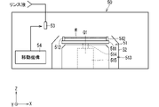
- FIG. 7 is a diagram schematically showing an example of the configuration of the single-wafer processing section 50.
- the single-wafer processing section 50 includes a substrate holding section 51 .
- the substrate holding part 51 holds the substrate W in a horizontal posture.
- the substrate holder 51 includes a stage 511 and multiple chuck pins 512 .
- the stage 511 has a disk shape and is provided in the negative direction of the Z-axis from the substrate W. As shown in FIG.
- the stage 511 is provided in a posture in which its thickness direction is along the Z-axis direction.
- a plurality of chuck pins 512 are provided on the main surface (that is, the upper surface) of the stage 511 in the Z-axis positive direction.
- Each chuck pin 512 is provided so as to be displaceable between a chuck position in contact with the periphery of the substrate W and a release position away from the periphery of the substrate W.
- the plurality of chuck pins 512 hold the substrate W when the plurality of chuck pins 512 move to their respective chuck positions.
- the substrate W is released from being held.
- the substrate holder 51 further includes a rotation mechanism 513, which rotates the substrate W around the rotation axis Q1.
- the rotation axis Q1 is an axis passing through the center of the substrate W and along the Z-axis direction.
- rotation mechanism 513 includes shaft 514 and motor 515 .
- the end of the shaft 514 in the positive Z-axis direction (that is, the upper end) is connected to the main surface in the negative Z-axis direction (that is, the lower surface) of the stage 511 and extends from the lower surface of the stage 511 along the rotation axis Q1.
- the motor 515 rotates the shaft 514 around the rotation axis Q1 to rotate the stage 511 and the plurality of chuck pins 512 together.
- the substrate W held by the plurality of chuck pins 512 rotates around the rotation axis Q1.
- Such a substrate holding part 51 can also be called a spin chuck.
- the substrate holding part 51 rotates the substrate W around the rotation axis Q1 at high speed, so that the liquid adhering to the substrate W can be scattered from the periphery of the substrate W and the substrate W can be dried (so-called spin drying).
- the single-wafer processing unit 50 also includes a guard 52.
- the guard 52 has a tubular shape and surrounds the substrate W held by the substrate holding part 51 .
- the guard 52 receives the liquid splashed from the peripheral edge of the substrate W.
- the single-wafer processing unit 50 also includes nozzles 53 .
- the nozzle 53 is used to supply pure water, isopropyl alcohol, or the like to the substrate W.
- FIG. The nozzle 53 is provided so as to be movable between a nozzle processing position and a nozzle standby position by a moving mechanism 54 .
- the nozzle processing position is, for example, a position facing the central portion of the surface of the substrate W in the Z-axis direction
- the nozzle standby position is, for example, a position radially outward of the substrate W.
- the movement mechanism 54 has, for example, a mechanism such as a ball screw mechanism or an arm turning mechanism. Pure water, isopropyl alcohol, or the like is discharged onto the rotating substrate W while the nozzle 53 is positioned at the nozzle processing position. As a result, the liquid that has landed on the surface of the substrate W receives centrifugal force, spreads over the entire surface of the substrate W, and scatters outward from the peripheral edge of the substrate W. As shown in FIG.
- the batch sheet-to-sheet transfer unit 70 includes a transfer robot 74 and a transfer robot 73 .
- the transport robot 74 is provided movably in the X-axis direction.
- the transport robot 74 can move to a position facing the batch processing section 30c.
- the transport robot 74 includes a hand 741 , and by moving the hand 741 , the substrate W in the horizontal posture is taken out from the transport robot 66 .
- the transport robot 74 may include a plurality of hands 741. In this case, the transport robot 74 may take out a plurality of substrates W using the hand 741 . If the number of hands 741 equal to or greater than the number of substrates W held by the transport robot 66 is provided, the transport robot 74 may take out all the substrates W held by the transport robot 66 .
- the transport robot 73 may take out the substrate W directly from the transport robot 74, a relay unit 75 is provided in the example of FIG.
- the relay unit 75 is provided in the Y-axis negative direction with respect to the transport robot 74 .
- the relay unit 75 includes a stationary storage container (not shown) that stores a plurality of substrates W in a horizontal posture side by side in the Z-axis direction.
- the transport robot 74 stores a plurality of horizontal substrates W in the storage container of the relay unit 75 .
- the transport robot 73 is provided in the Y-axis negative direction from the relay unit 75 .
- the transport robot 73 includes a hand 731 , and by moving the hand 731 , sequentially picks up the substrates W from the relay unit 75 and transports the substrates W to the individual wafer processing units 50 .
- the transport robot 73 may include multiple hands 731 .
- the transport robot 73 is provided movably along the Y-axis direction, and a plurality of single-wafer processing units 50 are arranged side by side along the Y-axis direction on each side of the transport path.
- the transport robot 73 sequentially takes out the dried substrates W from the respective single-wafer processing units 50 and sequentially transports them to the relay unit 75 .
- the relay unit 75 As a result, all the substrates W in the relay unit 75 are eventually replaced with substrates W that have been dried.
- the transport robot 74 collectively takes out a plurality of substrates W that have been dried from the relay unit 75 and transports the plurality of substrates W to the transport robot 21 via the relay unit 12 . Then, the transport robot 21 transports the plurality of substrates W to the carrier C1.
- FIG. 8 is a diagram schematically showing an example of the configuration of the transport robot 66 and its surroundings.
- a shielding plate 81 may be provided in the Z-axis positive direction relative to the transport robot 66 and in the Z-axis negative direction relative to the fan filter unit 80 .
- the fan filter unit 80 is provided in the upper part of the housing 100 and includes a fan and a filter (for example, a high-efficiency a particulate air filter (HEPA) filter).
- HEPA particulate air filter
- the shield plate 81 is provided at a position facing the plurality of substrates W held by the transport robot 66 in the Z-axis direction, and covers the plurality of substrates W held by the transport robot 66 in plan view. That is, the outline of the shielding plate 81 in plan view surrounds both the substrates W immediately before the attitude change and the substrates W immediately after the attitude change.
- the airflow from the fan filter unit 80 is blocked by the shield plate 81, so that the airflow can be prevented from acting on the plurality of substrates W held by the transfer robot 66. Therefore, drying of the substrate W caused by the airflow can be suppressed, and collapse of the three-dimensional structure of the substrate W caused by drying can be suppressed.
- the shield plate 81 may be movable integrally with the transport robot 66 .
- the shielding plate 81 may be attached to the base 662 of the transfer robot 66 via a fixing member (not shown). According to this, regardless of the position of the transport robot 66, the shielding plate 81 is positioned directly above the plurality of substrates W held by the transport robot 66, so that the plurality of substrates W are reliably prevented from being hit by the air current. can do.
- the shielding plate 81 may be immovably fixed to the housing 100 of the substrate processing apparatus 10 .
- the shield plate 81 may be provided over the entire movement area of the transport robot 66 .
- the transfer robot 66 is provided with the posture changing function.
- a configuration (posture conversion unit) for performing posture conversion may be separately provided.
- a mechanism for changing the posture in the posture changing section can be realized by a mechanism similar to the holding member 661 in the transfer robot 66, for example.
- the shielding plate 81 is positioned above the posture changing portion (for example, in the shape of a lid that covers the posture changing portion). , the plurality of substrates W can be reliably prevented from being hit by the airflow.
- the substrates W that have been subjected to the chemical treatment and the rinse treatment in the batch processing section 30 are transported to the single wafer processing section 50 while suppressing the waiting time, and the drying processing is performed in the single wafer processing section 50. , the start time of the chemical treatment will be described.
- the single-wafer processing unit 50 When the single-wafer processing unit 50 is processing the substrate at the timing after the substrate processing is performed in the batch processing unit 30 (when a plurality of single-wafer processing units 50 are provided, all of them are processing the substrate). If there is, ie, if there is no space in the single-wafer processing unit 50, the substrates W that have undergone substrate processing in the batch processing unit 30 need to wait at a predetermined location.
- such a waiting place for substrates W is assumed to be inside the processing tank 31 of the batch processing section 30b for the rinse liquid.
- the substrates W are prevented from being dried during the waiting period. Damage (collapse) can be suppressed.
- the following relationship holds between the substrate processing in the batch processing section 30, the substrate processing in the single wafer processing section 50, and the waiting time.
- TR indicates the remaining time of rinsing processing in the batch processing section 30b
- TTL indicates the time from the waiting place of substrates W (in this embodiment, inside the processing tank 31 of the batch processing section 30b) to the single wafer processing section 50.
- TSL indicates the time required for movement, and TSL is the longest remaining time of substrate processing (drying processing in this embodiment) in progress in the plurality of single-wafer processing units 50 (the single-wafer processing unit 50 If there is one, CN indicates the remaining time of the ongoing substrate processing in that single wafer processing unit 50), and CN indicates the number of substrates W waiting in the standby place, which is the number of single wafer processing units 50.
- the rounded up integer value of the value divided by TP indicates the time required for substrate processing (drying processing in the present embodiment) in the single-wafer processing section 50
- TP indicates the time required for chemical processing in the batch processing section 30
- TD indicates the waiting place for substrates W (this embodiment indicates the waiting time in the processing tank 31 of the batch processing section 30b.
- the number of substrates W after the chemical liquid treatment is performed and before the drying treatment is performed in the single-wafer processing unit 50 is defined as the standby number.
- the number of waiting wafers is the number of wafers W waiting at the waiting place.
- FIG. 9 is a conceptual diagram schematically showing the relationship of formula (1).
- the time required for the substrates W waiting in the standby place to finish the substrate processing in the single-wafer processing unit 50 is defined as the required time.
- the total on the left side corresponds to the required time.
- CN corresponds to the number of repetitions of substrate processing required until all the substrates W distributed to the single-wafer processing unit 50 are completely processed. Further, although the number of the single-wafer processing units 50 is four in the present embodiment, the number of the single-wafer processing units 50 may be one or more.
- TTL which is the time required for the substrate W to move from the standby location to the single-wafer processing unit 50, also includes the time required for the posture change of the substrate W performed by the transport robot 66.
- the waiting time (TD) for the substrates W that have undergone chemical processing in the batch processing section 30 it is possible to calculate the waiting time (TD) for the substrates W that have undergone chemical processing in the batch processing section 30 to wait at the standby location.
- the start time of the chemical solution processing in the batch processing unit 30 is delayed longer than the waiting time (TD) calculated with reference to the above formula (1), the time required for the chemical solution processing in the batch processing unit 30 is The required time (total of the left side) is shorter than (TP). Therefore, the substrate W for which the chemical treatment is started at the delayed timing is smoothly transported to the single-wafer processing section 50 without waiting in the batch processing section 30b, and the drying processing is performed in the single-wafer processing section 50. It will happen.
- the substrates W that have been subjected to the chemical treatment and the rinse treatment in the batch processing section 30 are transported to the single wafer processing section 50 while suppressing the waiting time, and the drying processing is performed in the single wafer processing section 50. , the number of substrates W to be processed with the chemical solution.
- the substrate processing in the batch processing section 30, the substrate processing in the single-wafer processing section 50, and the waiting time of the substrate W have a relationship such as the formula (1), but the batch processing section 30 Also by controlling the number of substrates W to be processed with the chemical solution (the number of substrates W to be processed WI), it is possible to suppress an increase in the number of substrates W waiting at the standby place.
- FIG. 10 is a conceptual diagram schematically showing the relationship of formula (2) below.
- CN is a rounded integer value obtained by dividing the number of substrates W on standby by the number of single-wafer processing units 50. Therefore, by multiplying the calculated CN by the number of single-wafer processing units 50, the number of substrates W It is possible to roughly calculate the number of processed sheets WI.
- the required time is reduced from the time required for the chemical processing in the batch processing unit 30. is also shorter.
- FIG. 11 is a plan view schematically showing an example of the configuration of a substrate processing apparatus 10A according to this embodiment.
- the Z-axis direction is the vertically upward direction.
- the substrate processing apparatus 10A is an apparatus that performs wet processing on substrates W. As shown in FIG.
- the substrate processing apparatus 10A includes a batch processing section 130 that collectively processes a plurality of substrates W, a single substrate processing section 50, an inter-batch transfer section 60, a batch and an inter-sheet conveying unit 70 .
- a chemical liquid batch processing unit 30a and a standby batch processing unit 30c are provided as the plurality of batch processing units 130.
- the batch processing section 30c includes a processing tank 31 and a lifter 32 like the batch processing section 30a.
- a processing solution eg, phosphoric acid at room temperature
- a plurality of substrates W after the chemical solution processing wait in the batch processing section 30 c until they are transported to the single wafer processing section 50 .
- the inter-batch transfer section 60 receives a plurality of chemically treated substrates W from the batch processing section 30a and transfers the received plurality of substrates W to the batch processing section 30c.
- the plurality of substrates W are transported with the processing liquid (here, the chemical liquid) adhered thereto. Therefore, during this transport, it is possible to suppress the collapse of the three-dimensional structure (for example, the insulating film 91) of the substrate W due to drying.
- the batch inter-wafer transfer unit 70 is provided in the Y-axis negative direction with respect to the batch processing unit 30c.
- the batch-to-single-wafer transfer unit 70 receives a plurality of substrates W taken out from the batch processing unit 30c by the batch-to-batch transfer unit 60, and transfers each substrate W to the single-wafer processing unit 50 one by one.
- the single-wafer processing unit 50 performs rinsing and drying on the substrate W. As for the drying process, the single-wafer processing unit 50 dries the substrates W one by one, so the substrates W can be dried with higher drying performance. Therefore, collapse of the three-dimensional structure of the substrate W due to drying can be suppressed.
- the single-wafer processing unit 50 When the single-wafer processing unit 50 is processing the substrate at the timing after the substrate processing is performed in the batch processing unit 130 (when a plurality of single-wafer processing units 50 are provided, all of them are processing the substrate). If there is, ie, if there is no space in the single-wafer processing unit 50, the substrates W that have undergone substrate processing in the batch processing unit 130 need to wait at a predetermined location.
- such a standby place for substrates W is assumed to be inside the processing tank 31 of the batch processing section 30c for the rinse liquid.
- a non-reactive chemical solution is stored in the processing tank 31 of the batch processing section 30c where the substrates W are waiting, the substrates W are prevented from being dried while they are waiting. damage (collapse) of the pattern formed on the surface of the .
- the following relationship holds between the substrate processing in the batch processing section 130, the substrate processing in the single wafer processing section 50, and the waiting time.
- TTL indicates the time required for the substrate W to move from the waiting place (in the processing tank 31 of the batch processing section 30c in this embodiment) to the single wafer processing section 50
- TSL The longest remaining time of the substrate processing (rinsing processing and drying processing in this embodiment) in progress in the processing section 50
- the single wafer processing CN indicates the number of substrates W waiting in the waiting area (waiting number) divided by the number of single-wafer processing units 50, rounded up to an integer value ( That is, if the decimal point is not 0, the integer part is incremented by 1, and the value after the decimal point is rounded to 0)
- TS is the substrate processing in each single wafer processing unit 50 ( In the present embodiment, rinsing processing and drying processing) are shown
- TP is the time required for the chemical liquid processing in the batch processing section 130
- TD is the waiting place for the substrate W (the batch processing section in the present embodiment). 30c) in the processing tank 31).
- FIG. 12 is
- the required time which is the time required for the substrate W waiting in the standby place to finish the substrate processing in the single-wafer processing unit 50, corresponds to the sum of the left sides in the above equation (3).
- the waiting time (TD) for the substrates W that have undergone chemical processing in the batch processing section 130 it is possible to calculate the waiting time (TD) for the substrates W that have undergone chemical processing in the batch processing section 130 to wait at the standby location. Therefore, if the start time of the chemical processing in the batch processing unit 130 is delayed longer than the waiting time (TD) calculated with reference to the above equation (3), the time (TP) required for the chemical processing in the batch processing unit 130 is The required time (total of the left side) is shorter than Therefore, the substrate W for which the chemical treatment is started at the delayed timing is smoothly transported to the single-wafer processing unit 50 without waiting in the batch processing unit 30c, and is rinsed and dried in the single-wafer processing unit 50. will be performed.
- substrates W that have undergone chemical treatment in the batch processing unit 130 are transported to the single wafer processing unit 50 while suppressing the waiting time, and rinse processing and drying processing are performed in the single wafer processing unit 50. , the number of substrates W to be processed with the chemical solution.
- the substrate processing in the batch processing section 130, the substrate processing in the single-wafer processing section 50, and the waiting time of the substrate W have a relationship such as Equation (3). Also by controlling the number of substrates W to be processed with the chemical solution (the number of substrates W to be processed WI), it is possible to suppress an increase in the number of substrates W waiting at the standby place.
- FIG. 13 is a conceptual diagram schematically showing the relationship of Equation (4) below.
- the required time is reduced from the time required for the chemical processing in the batch processing unit 130. is also shorter.
- the replacement may be made across multiple embodiments. In other words, it may be the case that the respective configurations whose examples are shown in the different embodiments are combined to produce the same effect.
- the batch processing unit 30 (or the batch processing unit 130) that performs substrate processing including chemical liquid processing on a plurality of substrates W, and the substrate processing including drying processing on one substrate W.
- a substrate processing method for processing a substrate using at least one single wafer processing unit 50 for processing includes the following steps. That is, according to the number of substrates W on standby, which is the number of substrates W after the chemical solution processing is performed in the batch processing unit 30 and before the drying processing is performed in the single wafer processing unit 50, the substrates W are transferred to the single wafer processing unit. a step of calculating the required time, which is the time required to finish the substrate processing, in 50; and controlling the time.
- the required time includes the remaining time of the ongoing substrate processing.
- the required time can be calculated taking into account the remaining time of the ongoing cleaning processing and drying processing. can be calculated with higher accuracy. Therefore, it is possible to shorten the waiting time of the substrates to be processed in the single-wafer processing section 50 after the substrate processing in the batch processing section 30 .
- the substrate processing method includes the following steps. That is, according to the number of substrates W on standby, which is the number of substrates W after the chemical solution processing is performed in the batch processing unit 30 and before the drying processing is performed in the single wafer processing unit 50, the substrates W are transferred to the single wafer processing unit. a step of calculating the required time, which is the time required to finish the substrate processing in 50; and changing the number of sheets.
- the substrate processing method includes the step of immersing a plurality of substrates W after being subjected to chemical processing in a cleaning bath in the batch processing section 30 to perform cleaning processing.
- the cleaning tank corresponds to, for example, the processing tank 31 in the batch processing section 30b.
- the step of calculating the required time is a step of calculating the required time including the time required for the cleaning process according to the number of waiting substrates W immersed in the processing tank 31 in the batch processing section 30b.
- the pattern formed on the surface of the substrate W can be prevented from collapsing.
- the rinsing process is collectively performed on a plurality of substrates W in the batch processing section 30, the time required for the rinsing process is shortened, and the time required for the entire substrate processing is also shortened.
- the substrate processing method includes the step of performing the cleaning process on the substrate W before the drying process is performed in the single-wafer processing unit 50 .
- the rinsing process is performed in the single-wafer processing unit 50, it is possible to perform the rinsing process with a high degree of freedom according to the properties of the substrate W and with a reduced consumption of the rinsing liquid. can.
- the step of calculating the required time is the number of waiting substrates W before moving from the batch processing unit 130 to the single-wafer processing unit 50. This is a step of calculating the required time including time. According to such a configuration, the overall substrate processing performed by the batch processing section 30 and the single substrate processing section 50 can be efficiently advanced.
- the chemical solution processing in the batch processing section 30 is performed by immersing the substrate W in the chemical solution bath.
- the chemical bath corresponds to, for example, the processing bath 31 in the batch processing section 30a.
- the substrate processing method includes a step of immersing the plurality of substrates W, which have been subjected to chemical treatment in the batch processing section 30, in the processing tank 31 in the batch processing section 30b to perform cleaning processing.
- the processing tank 31 in the batch processing section 30a has a first area where the chemical treatment is started at a first start time, and a second start time where the chemical treatment is different from the first start time.
- the processing tank 31 in the batch processing section 30b has a third region for cleaning the substrates W that have been chemically processed in the first region, and a second region. and a fourth area for performing cleaning processing on the substrate W that has been chemically processed in .
- substrate processing proceeds at different timings in a plurality of areas in the single processing tank 31, thereby increasing the degree of freedom in terms of the number of substrates W to be processed or the content of substrate processing.
- the maximum number of substrates W required to be processed in the single wafer processing section 50 is reduced. As a result, it is possible to effectively shorten the waiting time of the substrate W to be processed in the single-wafer processing section 50 after the substrate processing in the batch processing section 30 .
- the required time includes the time required for the substrate W to move from the batch processing section 30 to the single wafer processing section 50 .
- the entire substrate processing performed by the batch processing unit 30 and the single wafer processing unit 50 can be efficiently performed in consideration of the time required to move the substrate W from the batch processing unit 30 to the single wafer processing unit 50. can proceed accordingly.
- the required time includes the time required for attitude change for the substrate W processed in the batch processing section 30 to be processed in the single wafer processing section 50 .
- the batch processing unit 30 and the single-wafer processing unit 50 take into account the time required for changing the posture from the standing posture (vertical posture) suitable for batch processing to the horizontal posture suitable for single-wafer processing. The entire substrate processing can proceed efficiently.
- the required time is the number of substrates W that are repeatedly processed in one single wafer processing unit 50 when the number of substrates W on standby are distributed to a plurality of single wafer processing units 50. Includes processing time.
- the batch processing section 30 takes into account the number of repetitions of substrate processing required until the substrates W waiting are distributed to the single-wafer processing section 50 and the processing of all the substrates W is completed. And the entire substrate processing performed by the single-wafer processing section 50 can proceed efficiently.
- the material when a material name is described without being specified, unless there is a contradiction, the material contains other additives, such as an alloy. shall be included.
- Reference Signs List 10 10A substrate processing apparatus 11 load port 12, 75 relay unit 20 indexer transport section 21, 65, 66, 73, 74 transport robot 30, 30a, 30b, 30c, 130 batch processing section 31 processing tank 32 lifter 33, 611, 661 holding member 34, 662 base 35 lifting mechanism 50 single wafer processing section 51 substrate holding section 52 guard 53 nozzle 54, 665 moving mechanism 60 inter-batch transfer section 70 batch transfer section between single wafers 80 fan filter unit 81 shielding plate 90 laminated structure 91 insulating film 92 sacrificial film 93 support layer 94 trench 100 housing 211, 731, 741 hand 212 upright support member 511 stage 512 chuck pin 513, 664 rotation mechanism 514 shaft 515 motor 613, 663 opening and closing mechanism 6611 contact member 6612 support member 6613 rotating member
Landscapes
- Cleaning Or Drying Semiconductors (AREA)
- Container, Conveyance, Adherence, Positioning, Of Wafer (AREA)
- Chemical & Material Sciences (AREA)
- Chemical Kinetics & Catalysis (AREA)
- General Chemical & Material Sciences (AREA)
- Weting (AREA)
Abstract
Description
以下、本実施の形態に関する基板処理方法について説明する。
図1は、本実施の形態に関する、基板処理装置10の構成の一例を概略的に示す平面図である。図1において、Z軸方向が鉛直上方向である。基板処理装置10は、基板Wに対してウェット処理を行う装置である。
図3は、本実施の形態に関する、基板Wに対する処理工程の一例を概略的に示すフローチャートである。図3に例が示されるように、まず、複数の基板Wに対して、バッチ式の薬液処理が行われる(ステップST1)。
以下、基板処理装置10のそれぞれの構成の具体的な一例について述べる。
図1の例では、インデクサ搬送部20は搬送ロボット21を含んでいる。搬送ロボット21は、ロードポート11よりもX軸正方向において、Y軸方向に沿って移動可能に設けられている。搬送ロボット21は、ロードポート11に載置されたそれぞれのキャリアC1とX軸方向において向かい合う位置で停止することができる。
次に、バッチ処理部30について説明する。図1の例では、複数のバッチ処理部30は、X軸方向に沿って一列に配列されている。
バッチ間搬送部60は、搬送ロボット65と搬送ロボット66とを含んでいる。図4の例では、バッチ間搬送部60の搬送ロボット65は、一対の保持部材611と開閉機構613とを含む。
図7は、枚葉処理部50の構成の一例を概略的に示す図である。枚葉処理部50は、基板保持部51を含んでいる。基板保持部51は、基板Wを水平姿勢で保持する。図7の例では、基板保持部51は、ステージ511と複数のチャックピン512とを含んでいる。ステージ511は円板形状を有し、基板WよりもZ軸負方向に設けられる。ステージ511は、その厚み方向がZ軸方向に沿う姿勢で設けられる。
図1の例では、バッチ枚葉間搬送部70は、搬送ロボット74と搬送ロボット73とを含んでいる。
図8は、搬送ロボット66およびその周辺の構成の一例を概略的に示す図である。図8に例示するように、搬送ロボット66よりもZ軸正方向、かつ、ファンフィルターユニット80よりもZ軸負方向には、遮蔽板81が設けられていてもよい。ファンフィルターユニット80は、筐体100の上部に設けられ、かつ、クリーンルーム内の空気を取り込んで当該空気を筐体100内の枚葉処理部50などに送り出すためのファンおよびフィルタ(たとえば、high efficiency particulate air filter(HEPA)フィルタ)を備える。
以下、バッチ処理部30で薬液処理およびリンス処理が行われた後の基板Wを、待ち時間を抑制しつつ枚葉処理部50に搬送して、枚葉処理部50において乾燥処理を行うための、薬液処理の開始時刻について説明する。

以下、バッチ処理部30で薬液処理およびリンス処理が行われた後の基板Wを、待ち時間を抑制しつつ枚葉処理部50に搬送して、枚葉処理部50において乾燥処理を行うための、薬液処理が行われる基板Wの枚数について説明する。

本実施の形態に関する基板処理方法について説明する。なお、以下の説明においては、以上に記載された実施の形態で説明された構成要素と同様の構成要素については同じ符号を付して図示し、その詳細な説明については適宜省略するものとする。
図11は、本実施の形態に関する、基板処理装置10Aの構成の一例を概略的に示す平面図である。図1において、Z軸方向が鉛直上方向である。基板処理装置10Aは、基板Wに対してウェット処理を行う装置である。
以下、バッチ処理部130で薬液処理が行われた後の基板Wを、待ち時間を抑制しつつ枚葉処理部50に搬送して、枚葉処理部50においてリンス処理および乾燥処理を行うための、薬液処理の開始時刻について説明する。

以下、バッチ処理部130で薬液処理が行われた後の基板Wを、待ち時間を抑制しつつ枚葉処理部50に搬送して、枚葉処理部50においてリンス処理および乾燥処理を行うための、薬液処理が行われる基板Wの枚数について説明する。

次に、以上に記載された実施の形態によって生じる効果の例を示す。なお、以下の説明においては、以上に記載された実施の形態に例が示された具体的な構成に基づいて当該効果が記載されるが、同様の効果が生じる範囲で、本願明細書に例が示される他の具体的な構成と置き換えられてもよい。すなわち、以下では便宜上、対応づけられる具体的な構成のうちのいずれか1つのみが代表して記載される場合があるが、代表して記載された具体的な構成が対応づけられる他の具体的な構成に置き換えられてもよい。
以上に記載された実施の形態では、それぞれの構成要素の材質、材料、寸法、形状、相対的配置関係または実施の条件などについても記載する場合があるが、これらはすべての局面においてひとつの例であって、限定的なものではないものとする。
11 ロードポート
12,75 中継ユニット
20 インデクサ搬送部
21,65,66,73,74 搬送ロボット
30,30a,30b,30c,130 バッチ処理部
31 処理槽
32 リフタ
33,611,661 保持部材
34,662 ベース
35 昇降機構
50 枚葉処理部
51 基板保持部
52 ガード
53 ノズル
54,665 移動機構
60 バッチ間搬送部
70 バッチ枚葉間搬送部
80 ファンフィルターユニット
81 遮蔽板
90 積層構造
91 絶縁膜
92 犠牲膜
93 支持層
94 トレンチ
100 筐体
211,731,741 ハンド
212 起立支持部材
511 ステージ
512 チャックピン
513,664 回転機構
514 シャフト
515 モータ
613,663 開閉機構
6611 接触部材
6612 支持部材
6613 回転部材
Claims (10)
- 複数の基板に対する薬液処理を含む基板処理を行うバッチ処理部と、1枚の前記基板に対する乾燥処理を含む前記基板処理を行う少なくとも1つの枚葉処理部とを使って前記基板処理を行う基板処理方法であり、
前記バッチ処理部において前記薬液処理が行われた後で、かつ、前記枚葉処理部において前記乾燥処理が行われる前の前記基板の枚数である待機枚数に応じて、前記基板が前記枚葉処理部における前記基板処理を終えるまでにかかる時間である所要時間を算出する工程と、
前記所要時間が、前記バッチ処理部における前記薬液処理にかかる時間よりも短くなるように、前記バッチ処理部における前記薬液処理の開始時刻を制御する工程とを備える、
基板処理方法。 - 請求項1に記載の基板処理方法であり、
前記所要時間には、進行中の前記基板処理の残り時間を含む、
基板処理方法。 - 複数の基板に対する薬液処理を含む基板処理を行うバッチ処理部と、1枚の前記基板に対する乾燥処理を含む前記基板処理を行う少なくとも1つの枚葉処理部とを使って前記基板処理を行う基板処理方法であり、
前記バッチ処理部において前記薬液処理が行われた後で、かつ、前記枚葉処理部において前記乾燥処理が行われる前の前記基板の枚数である待機枚数に応じて、前記基板が前記枚葉処理部における前記基板処理を終えるまでにかかる時間である所要時間を算出する工程と、
前記所要時間が、前記バッチ処理部における前記薬液処理にかかる時間よりも短くなるように、前記バッチ処理部における前記基板の処理枚数を変更する工程とを備える、
基板処理方法。 - 請求項1から3のうちのいずれか1つに記載の基板処理方法であり、
前記バッチ処理部において、前記薬液処理が行われた後の複数の前記基板を洗浄槽に浸漬させて洗浄処理を行う工程をさらに備え、
前記所要時間を算出する工程は、前記洗浄槽に浸漬している前記基板の前記待機枚数に応じて、前記洗浄処理にかかる時間を含む前記所要時間を算出する工程である、
基板処理方法。 - 請求項1から3のうちのいずれか1つに記載の基板処理方法であり、
前記枚葉処理部において、前記乾燥処理が行われる前の前記基板に洗浄処理を行う工程をさらに備える、
基板処理方法。 - 請求項5に記載の基板処理方法であり、
前記所要時間を算出する工程は、前記バッチ処理部から前記枚葉処理部まで移動する前の前記基板の前記待機枚数に応じて、前記洗浄処理にかかる時間を含む前記所要時間を算出する工程である、
基板処理方法。 - 請求項1から6のうちのいずれか1つに記載の基板処理方法であり、
前記バッチ処理部における前記薬液処理は、前記基板を薬液槽に浸漬させて行われ、
前記バッチ処理部において、前記薬液処理が行われた後の複数の前記基板を洗浄槽に浸漬させて洗浄処理を行う工程をさらに備え、
前記薬液槽は、前記薬液処理が第1の開始時刻で開始される第1の領域と、前記薬液処理が前記第1の開始時刻とは異なる時刻である第2の開始時刻で開始される第2の領域とを備え、
前記洗浄槽は、前記第1の領域で前記薬液処理が行われた前記基板に前記洗浄処理を行う第3の領域と、前記第2の領域で前記薬液処理が行われた前記基板に前記洗浄処理を行う第4の領域とを備える、
基板処理方法。 - 請求項1から7のうちのいずれか1つに記載の基板処理方法であり、
前記所要時間は、前記基板が前記バッチ処理部から前記枚葉処理部まで移動するためにかかる時間を含む、
基板処理方法。 - 請求項1から8のうちのいずれか1つに記載の基板処理方法であり、
前記所要時間は、前記バッチ処理部において前記基板処理された前記基板が前記枚葉処理部において前記基板処理されるための姿勢変換にかかる時間を含む、
基板処理方法。 - 請求項1から9のうちのいずれか1つに記載の基板処理方法であり、
前記所要時間は、前記待機枚数の前記基板が複数の前記枚葉処理部に分配された場合の、1つの前記枚葉処理部において繰り返し行われる前記基板処理にかかる時間を含む、
基板処理方法。
Priority Applications (4)
| Application Number | Priority Date | Filing Date | Title |
|---|---|---|---|
| KR1020237038870A KR102871618B1 (ko) | 2021-05-20 | 2022-05-16 | 기판 처리 방법 |
| CN202280036083.2A CN117321737A (zh) | 2021-05-20 | 2022-05-16 | 基板处理方法 |
| US18/560,099 US20240234189A1 (en) | 2021-05-20 | 2022-05-16 | Substrate processing method |
| EP22804656.1A EP4343819A4 (en) | 2021-05-20 | 2022-05-16 | SUBSTRATE TREATMENT METHOD |
Applications Claiming Priority (2)
| Application Number | Priority Date | Filing Date | Title |
|---|---|---|---|
| JP2021-085328 | 2021-05-20 | ||
| JP2021085328A JP7650722B2 (ja) | 2021-05-20 | 2021-05-20 | 基板処理方法 |
Publications (1)
| Publication Number | Publication Date |
|---|---|
| WO2022244745A1 true WO2022244745A1 (ja) | 2022-11-24 |
Family
ID=84141363
Family Applications (1)
| Application Number | Title | Priority Date | Filing Date |
|---|---|---|---|
| PCT/JP2022/020422 Ceased WO2022244745A1 (ja) | 2021-05-20 | 2022-05-16 | 基板処理方法 |
Country Status (7)
| Country | Link |
|---|---|
| US (1) | US20240234189A1 (ja) |
| EP (1) | EP4343819A4 (ja) |
| JP (1) | JP7650722B2 (ja) |
| KR (1) | KR102871618B1 (ja) |
| CN (1) | CN117321737A (ja) |
| TW (1) | TWI827036B (ja) |
| WO (1) | WO2022244745A1 (ja) |
Cited By (1)
| Publication number | Priority date | Publication date | Assignee | Title |
|---|---|---|---|---|
| US20240413001A1 (en) * | 2023-06-08 | 2024-12-12 | SCREEN Holdings Co., Ltd. | Substrate processing apparatus |
Families Citing this family (6)
| Publication number | Priority date | Publication date | Assignee | Title |
|---|---|---|---|---|
| KR102858825B1 (ko) * | 2022-06-24 | 2025-09-15 | 세메스 주식회사 | 버퍼 챔버, 기판 처리 장치 및 기판 처리 방법 |
| JP7624466B2 (ja) * | 2023-01-27 | 2025-01-30 | 株式会社Screenホールディングス | 基板処理システム |
| JP7733061B2 (ja) * | 2023-06-08 | 2025-09-02 | 株式会社Screenホールディングス | 液中姿勢変換装置及びそれを備えた基板処理装置 |
| JP7733066B2 (ja) * | 2023-06-27 | 2025-09-02 | 株式会社Screenホールディングス | 基板処理システム |
| JP7796703B2 (ja) * | 2023-07-25 | 2026-01-09 | 株式会社Screenホールディングス | 姿勢変換装置及びそれを備えた基板処理装置 |
| JP7811569B2 (ja) * | 2023-11-29 | 2026-02-05 | 株式会社Screenホールディングス | 基板処理システムおよび基板処理方法 |
Citations (7)
| Publication number | Priority date | Publication date | Assignee | Title |
|---|---|---|---|---|
| JP2002118086A (ja) * | 2000-08-01 | 2002-04-19 | Tokyo Electron Ltd | 洗浄処理方法及び洗浄処理装置 |
| JP2003051481A (ja) * | 2001-08-07 | 2003-02-21 | Hitachi Ltd | 半導体集積回路装置の製造方法 |
| JP2006147779A (ja) * | 2004-11-18 | 2006-06-08 | Tokyo Electron Ltd | 処理システム |
| JP2008235813A (ja) * | 2007-03-23 | 2008-10-02 | Dainippon Screen Mfg Co Ltd | 基板処理装置 |
| US20200203193A1 (en) * | 2018-12-14 | 2020-06-25 | Xia Tai Xin Semiconductor (Qing Dao) Ltd. | Method and apparatus for cleaning semiconductor wafers |
| JP2021064654A (ja) * | 2019-10-10 | 2021-04-22 | 東京エレクトロン株式会社 | 基板処理システム、及び基板処理方法 |
| JP2021064652A (ja) * | 2019-10-10 | 2021-04-22 | 東京エレクトロン株式会社 | 基板処理システム、及び基板処理方法 |
Family Cites Families (8)
| Publication number | Priority date | Publication date | Assignee | Title |
|---|---|---|---|---|
| JP2725106B2 (ja) * | 1991-12-18 | 1998-03-09 | 大日本スクリーン製造株式会社 | 基板表面処理方法及び基板表面処理装置 |
| JP4467379B2 (ja) * | 2004-08-05 | 2010-05-26 | 大日本スクリーン製造株式会社 | 基板処理装置 |
| KR20060030677A (ko) * | 2004-10-06 | 2006-04-11 | 삼성전자주식회사 | 기판 건조 장치 및 방법 |
| US20060137726A1 (en) * | 2004-12-24 | 2006-06-29 | Dainippon Screen Mfg. Co., Ltd. | Substrate treating apparatus |
| KR101992660B1 (ko) | 2012-11-28 | 2019-09-30 | 에이씨엠 리서치 (상하이) 인코포레이티드 | 반도체 웨이퍼의 세정 방법 및 장치 |
| KR102440321B1 (ko) * | 2015-09-04 | 2022-09-06 | 삼성전자주식회사 | 기판 처리 방법 |
| JP6951269B2 (ja) * | 2018-01-29 | 2021-10-20 | 株式会社荏原製作所 | 基板処理装置、基板処理装置の制御装置、基板処理装置の制御方法、プログラムを格納した記憶媒体 |
| JP6899813B2 (ja) * | 2018-11-27 | 2021-07-07 | 株式会社Screenホールディングス | 基板処理装置および基板処理方法 |
-
2021
- 2021-05-20 JP JP2021085328A patent/JP7650722B2/ja active Active
-
2022
- 2022-05-04 TW TW111116743A patent/TWI827036B/zh active
- 2022-05-16 CN CN202280036083.2A patent/CN117321737A/zh active Pending
- 2022-05-16 EP EP22804656.1A patent/EP4343819A4/en active Pending
- 2022-05-16 KR KR1020237038870A patent/KR102871618B1/ko active Active
- 2022-05-16 US US18/560,099 patent/US20240234189A1/en active Pending
- 2022-05-16 WO PCT/JP2022/020422 patent/WO2022244745A1/ja not_active Ceased
Patent Citations (7)
| Publication number | Priority date | Publication date | Assignee | Title |
|---|---|---|---|---|
| JP2002118086A (ja) * | 2000-08-01 | 2002-04-19 | Tokyo Electron Ltd | 洗浄処理方法及び洗浄処理装置 |
| JP2003051481A (ja) * | 2001-08-07 | 2003-02-21 | Hitachi Ltd | 半導体集積回路装置の製造方法 |
| JP2006147779A (ja) * | 2004-11-18 | 2006-06-08 | Tokyo Electron Ltd | 処理システム |
| JP2008235813A (ja) * | 2007-03-23 | 2008-10-02 | Dainippon Screen Mfg Co Ltd | 基板処理装置 |
| US20200203193A1 (en) * | 2018-12-14 | 2020-06-25 | Xia Tai Xin Semiconductor (Qing Dao) Ltd. | Method and apparatus for cleaning semiconductor wafers |
| JP2021064654A (ja) * | 2019-10-10 | 2021-04-22 | 東京エレクトロン株式会社 | 基板処理システム、及び基板処理方法 |
| JP2021064652A (ja) * | 2019-10-10 | 2021-04-22 | 東京エレクトロン株式会社 | 基板処理システム、及び基板処理方法 |
Non-Patent Citations (1)
| Title |
|---|
| See also references of EP4343819A4 |
Cited By (1)
| Publication number | Priority date | Publication date | Assignee | Title |
|---|---|---|---|---|
| US20240413001A1 (en) * | 2023-06-08 | 2024-12-12 | SCREEN Holdings Co., Ltd. | Substrate processing apparatus |
Also Published As
| Publication number | Publication date |
|---|---|
| EP4343819A4 (en) | 2025-08-06 |
| EP4343819A1 (en) | 2024-03-27 |
| US20240234189A1 (en) | 2024-07-11 |
| KR102871618B1 (ko) | 2025-10-15 |
| JP7650722B2 (ja) | 2025-03-25 |
| TWI827036B (zh) | 2023-12-21 |
| CN117321737A (zh) | 2023-12-29 |
| KR20230167430A (ko) | 2023-12-08 |
| TW202303735A (zh) | 2023-01-16 |
| JP2022178486A (ja) | 2022-12-02 |
Similar Documents
| Publication | Publication Date | Title |
|---|---|---|
| WO2022244745A1 (ja) | 基板処理方法 | |
| CN101799624B (zh) | 基板处理装置 | |
| JP7181081B2 (ja) | 基板処理装置および基板搬送方法 | |
| JPH1074818A (ja) | 処理装置 | |
| JPH1084029A (ja) | 処理システム | |
| US20190096729A1 (en) | Substrate inverting device, substrate processing apparatus, and substrate catch-and-hold device | |
| JPH1079343A (ja) | 処理方法及び塗布現像処理システム | |
| WO2022244516A1 (ja) | 基板処理方法および基板処理装置 | |
| WO2022230805A1 (ja) | 基板処理装置 | |
| US20240334759A1 (en) | Substrate treating apparatus and substrate transporting method | |
| JP2013069874A (ja) | 基板処理システム、基板搬送方法、プログラム及びコンピュータ記憶媒体 | |
| US20250038028A1 (en) | Substrate processing system | |
| JP5378686B2 (ja) | 基板処理装置 | |
| TWM647657U (zh) | 晶圓濕式處理與清洗系統 | |
| TWI820699B (zh) | 基板處理方法以及基板處理裝置 | |
| WO2023139851A1 (ja) | 基板処理方法、および、基板処理装置 | |
| JP2006128209A (ja) | 基板処理装置 | |
| JP2008160021A (ja) | 基板搬送装置およびそれを備えた基板処理装置 | |
| JP2000114165A (ja) | 現像処理装置 |
Legal Events
| Date | Code | Title | Description |
|---|---|---|---|
| 121 | Ep: the epo has been informed by wipo that ep was designated in this application |
Ref document number: 22804656 Country of ref document: EP Kind code of ref document: A1 |
|
| ENP | Entry into the national phase |
Ref document number: 20237038870 Country of ref document: KR Kind code of ref document: A |
|
| WWE | Wipo information: entry into national phase |
Ref document number: 18560099 Country of ref document: US Ref document number: 1020237038870 Country of ref document: KR |
|
| WWE | Wipo information: entry into national phase |
Ref document number: 202280036083.2 Country of ref document: CN |
|
| WWE | Wipo information: entry into national phase |
Ref document number: 2022804656 Country of ref document: EP |
|
| NENP | Non-entry into the national phase |
Ref country code: DE |
|
| ENP | Entry into the national phase |
Ref document number: 2022804656 Country of ref document: EP Effective date: 20231220 |