WO2024202425A1 - Commutateur d'isolation et séquenceur - Google Patents
Commutateur d'isolation et séquenceur Download PDFInfo
- Publication number
- WO2024202425A1 WO2024202425A1 PCT/JP2024/001304 JP2024001304W WO2024202425A1 WO 2024202425 A1 WO2024202425 A1 WO 2024202425A1 JP 2024001304 W JP2024001304 W JP 2024001304W WO 2024202425 A1 WO2024202425 A1 WO 2024202425A1
- Authority
- WO
- WIPO (PCT)
- Prior art keywords
- circuit
- secondary coil
- coil
- signal
- switch
- Prior art date
- Legal status (The legal status is an assumption and is not a legal conclusion. Google has not performed a legal analysis and makes no representation as to the accuracy of the status listed.)
- Ceased
Links
Images


Classifications
-
- H—ELECTRICITY
- H03—ELECTRONIC CIRCUITRY
- H03K—PULSE TECHNIQUE
- H03K17/00—Electronic switching or gating, i.e. not by contact-making and –breaking
- H03K17/51—Electronic switching or gating, i.e. not by contact-making and –breaking characterised by the components used
- H03K17/56—Electronic switching or gating, i.e. not by contact-making and –breaking characterised by the components used by the use, as active elements, of semiconductor devices
- H03K17/687—Electronic switching or gating, i.e. not by contact-making and –breaking characterised by the components used by the use, as active elements, of semiconductor devices the devices being field-effect transistors
- H03K17/689—Electronic switching or gating, i.e. not by contact-making and –breaking characterised by the components used by the use, as active elements, of semiconductor devices the devices being field-effect transistors with galvanic isolation between the control circuit and the output circuit
- H03K17/691—Electronic switching or gating, i.e. not by contact-making and –breaking characterised by the components used by the use, as active elements, of semiconductor devices the devices being field-effect transistors with galvanic isolation between the control circuit and the output circuit using transformer coupling
-
- H—ELECTRICITY
- H03—ELECTRONIC CIRCUITRY
- H03K—PULSE TECHNIQUE
- H03K17/00—Electronic switching or gating, i.e. not by contact-making and –breaking
- H03K17/08—Modifications for protecting switching circuit against overcurrent or overvoltage
- H03K17/082—Modifications for protecting switching circuit against overcurrent or overvoltage by feedback from the output to the control circuit
-
- H—ELECTRICITY
- H03—ELECTRONIC CIRCUITRY
- H03K—PULSE TECHNIQUE
- H03K17/00—Electronic switching or gating, i.e. not by contact-making and –breaking
- H03K17/51—Electronic switching or gating, i.e. not by contact-making and –breaking characterised by the components used
- H03K17/56—Electronic switching or gating, i.e. not by contact-making and –breaking characterised by the components used by the use, as active elements, of semiconductor devices
- H03K17/687—Electronic switching or gating, i.e. not by contact-making and –breaking characterised by the components used by the use, as active elements, of semiconductor devices the devices being field-effect transistors
- H03K17/689—Electronic switching or gating, i.e. not by contact-making and –breaking characterised by the components used by the use, as active elements, of semiconductor devices the devices being field-effect transistors with galvanic isolation between the control circuit and the output circuit
-
- H—ELECTRICITY
- H03—ELECTRONIC CIRCUITRY
- H03K—PULSE TECHNIQUE
- H03K17/00—Electronic switching or gating, i.e. not by contact-making and –breaking
- H03K17/51—Electronic switching or gating, i.e. not by contact-making and –breaking characterised by the components used
- H03K17/74—Electronic switching or gating, i.e. not by contact-making and –breaking characterised by the components used by the use, as active elements, of diodes
-
- H—ELECTRICITY
- H03—ELECTRONIC CIRCUITRY
- H03K—PULSE TECHNIQUE
- H03K19/00—Logic circuits, i.e. having at least two inputs acting on one output; Inverting circuits
- H03K19/0175—Coupling arrangements; Interface arrangements
-
- H—ELECTRICITY
- H04—ELECTRIC COMMUNICATION TECHNIQUE
- H04L—TRANSMISSION OF DIGITAL INFORMATION, e.g. TELEGRAPHIC COMMUNICATION
- H04L25/00—Baseband systems
- H04L25/02—Details ; arrangements for supplying electrical power along data transmission lines
Definitions
- This disclosure relates to an insulating switch and a sequencer using an insulating switch. This disclosure also relates to a signal transmission device.
- signal transmission devices that transmit signals between a primary circuit system and a secondary circuit system while electrically insulating the primary circuit system and the secondary circuit system have been used in various applications (such as power supplies or motor drive devices).
- Patent Document 2 As an example of related prior art, see Patent Document 2 by the same applicant as the present application.
- JP 2020-096051 A International Publication No. 2022/070944
- conventional signal transmission devices can cause problems in transmitting signals from the primary circuit system to the secondary circuit system if the power supply for the primary circuit system is unstable or insufficient.
- the insulating switch includes a switch unit configured to be controlled between a conductive state and a non-conductive state, a conduction circuit configured to control the switch unit to the conductive state, an adjustment circuit configured to adjust at least the switch unit from the conductive state to the non-conductive state, and a pulse supply circuit configured to receive a control signal and supply a pulse signal to at least one of the conduction circuit and the adjustment circuit.
- the conduction circuit includes a first insulating element having a first primary coil connected to the pulse supply circuit and a first secondary coil electromagnetically coupled to the first primary coil, and is configured to bring the switch unit into a conductive state by an induced current flowing at the rising edge of the pulse signal supplied to the first primary coil.
- the adjustment circuit includes a second insulating element having a second primary coil connected to the pulse supply circuit and a second secondary coil electromagnetically coupled to the second primary coil, and an adjustment element that adjusts the voltage of the control terminal of the switch unit by an induced current flowing in the second secondary coil at the rising edge of the pulse signal to bring the switch unit into the non-conductive state.
- the pulse supply circuit is configured to supply the pulse signal to the first primary coil when the control signal is at a first level, and to supply the pulse signal to the second primary coil from the point in time when the control signal switches from the first level to a second level different from the first level, and to set the switch unit to the conductive state when the control signal is at the first level.
- a signal transmission device configured to transmit a signal between a primary circuit system and a secondary circuit system while isolating the primary circuit system and the secondary circuit system, and includes a first insulating element configured to transmit a first signal from the secondary circuit system to the primary circuit system, a second insulating element configured to transmit a second signal from the primary circuit system to the secondary circuit system, a drive circuit provided in the secondary circuit system and configured to drive the first insulating element, a switch circuit provided in the primary circuit system and configured to switch the connection state between the first insulating element and the second insulating element in response to an input signal, and a receiving circuit configured to detect the second signal and generate an output signal in response to the input signal.
- FIG. 1 is a diagram showing a basic configuration of a signal transmission device.
- FIG. 2 is a diagram showing the basic structure of a transformer chip.
- FIG. 3 is a perspective view of a semiconductor device used as a two-channel type transformer chip.
- FIG. 4 is a plan view of the semiconductor device shown in FIG.
- FIG. 5 is a plan view showing a layer in which the low potential coil is formed in the semiconductor device of FIG.
- FIG. 6 is a plan view showing a layer in which a high potential coil is formed in the semiconductor device of FIG.
- FIG. 7 is a cross-sectional view taken along line VIII-VIII shown in FIG.
- FIG. 8 is an enlarged view (isolation structure) of the region XIII shown in FIG.
- FIG. 9 is a diagram illustrating an example of the layout of a transformer chip.
- FIG. 10 is a diagram showing a first embodiment of a signal transmission device.
- FIG. 11 is a diagram illustrating a first operation example (intermittent) of the first embodiment.
- FIG. 12 is a diagram illustrating a second operation example (continuous) of the first embodiment.
- FIG. 13 is a diagram showing a second embodiment of a signal transmission device.
- FIG. 14 is a diagram showing a third embodiment of a signal transmission device.
- FIG. 15 is a diagram illustrating an operation example of the third embodiment.
- FIG. 16 is a diagram showing a fourth embodiment of a signal transmission device.
- FIG. 17 is a diagram showing a fifth embodiment of a signal transmission device.
- FIG. 10 is a diagram showing a first embodiment of a signal transmission device.
- FIG. 11 is a diagram illustrating a first operation example (intermittent) of the first embodiment.
- FIG. 12 is a diagram illustrating
- FIG. 18 is a diagram showing a sixth embodiment of a signal transmission device.
- FIG. 19 is a diagram illustrating an operation example of the sixth embodiment.
- FIG. 20 is a diagram showing a seventh embodiment of a signal transmission device.
- FIG. 21 is a diagram showing an eighth embodiment of a signal transmission device.
- FIG. 22 is a diagram showing an operation example of the eighth embodiment.
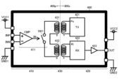
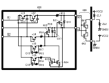
- FIG. 23 is a schematic circuit diagram of one form of an isolation switch according to an embodiment of the present disclosure.
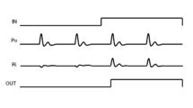
- FIG. 24 is a timing chart showing the operation of the isolation switch.
- FIG. 25 is a timing chart showing the operation of the isolation switch of the first modified example.
- FIG. 26 is a schematic circuit diagram of an isolation switch according to a second modified example.
- FIG. 27 is a timing chart showing the operation of the isolation switch of the second modified example.
- FIG. 28 is a schematic circuit diagram of an isolation switch according to a third modified example.
- FIG. 29 is a schematic circuit diagram of an isolation switch according to a fourth modified example.
- FIG. 30 is a schematic circuit diagram of an isolation switch according to a fifth modified example.
- FIG. 31 is a timing chart showing the operation of the isolation switch of the fifth modified example.
- FIG. 32 is a schematic circuit diagram of an isolation switch according to a sixth modified example.
- FIG. 331 is a schematic circuit diagram of another configuration example of the isolation switch of the sixth modified example.
- FIG. 34 is a schematic circuit diagram of an isolation switch according to a seventh modified example.
- FIG. 35 is a timing chart showing the operation of the isolation switch of the seventh modified example.
- FIG. 36 illustrates an additional embodiment of an isolation switch.
- FIG. 28 is a schematic circuit diagram of an isolation switch according to a third modified example.
- FIG. 29 is a schematic circuit diagram of an isolation switch according to a fourth modified example.
- FIG. 30 is a
- FIG. 37 is a diagram showing a first main part of an isolation switch according to an additional embodiment.
- FIG. 38 is a diagram showing an example of the operation of the first main part.
- FIG. 39 is a diagram showing a second main part of an isolation switch according to an additional embodiment.
- FIG. 40 is a diagram showing a third main part of an isolation switch according to an additional embodiment.
- FIG. 41 is a diagram showing a third tip in the third main portion.
- FIG. 42 is a diagram showing a modified example of the third main part.
- FIG. 43 is a diagram showing a third tip in a modified example of the third main part.
- FIG. 44 is a diagram showing a modified example of the second chip.
- FIG. 45 is a diagram showing an example of the operation of the second chip in the above modification.
- FIG. 45 is a diagram showing an example of the operation of the second chip in the above modification.
- FIG. 46 illustrates an additional embodiment of a signaling device.
- FIG. 47 is a diagram showing an example of the configuration of an isolated power supply circuit.
- FIG. 48 is a diagram showing a modified example of a signal transmission device according to an additional embodiment.
- FIG. 49 is a diagram showing a modified example of an isolated power supply circuit.
- FIG. 50 shows a modified example of an insulating element for percussion.
- connection includes mechanical connection as well as electrical connection, in other words, a state in which electricity flows.
- connection includes electrical connection.
- a line refers to a wiring through which an electrical signal is propagated or supplied.
- Ground potential refers to a reference conductive part having a reference potential of 0V (zero volts), or refers to the potential of 0V itself.
- the reference conductive part is formed of a conductor such as a metal.
- a potential of 0V is sometimes referred to as ground potential.
- a voltage indicated without any particular reference represents a potential seen from the ground potential.
- Level refers to the level of potential, and for any signal or voltage, the Hi level has a higher potential than the Lo level.
- Any digital signal has a signal level of Hi level or Lo level.
- a signal or voltage at Hi level strictly means that the signal or voltage level is at Hi level
- a signal or voltage at Lo level strictly means that the signal or voltage level is at Lo level.
- the level of a signal is sometimes expressed as a signal level
- the level of a voltage is sometimes expressed as a voltage level.
- the inverted signal of the signal is at Lo level
- the inverted signal of the signal is at Hi level.
- the Hi level may be referred to as the first level.
- the period during which the signal is Hi is called the Hi level period.
- the period during which the signal is Lo is called the Lo level period. The same applies to any voltage that has a Hi or Lo voltage level.
- a switching element can be in either an ON or OFF state.
- When a switching element is in the ON state there is electrical continuity between both ends of the switch.
- the period when a switching element is in the ON state is referred to as the ON period
- the period when a switching element is in the OFF state is referred to as the OFF period.
- switching to the ON state is sometimes referred to as turning ON
- switching to the OFF state is sometimes referred to as turning OFF.
- An example of a switching element may be a MOS (Metal Oxide Semiconductor) field effect transistor.
- MOS field effect transistor is a transistor whose gate structure consists of at least three layers: a layer made of a conductor or a semiconductor such as polysilicon with a low resistance value, an insulating layer, and a P-channel, N-channel, or intrinsic semiconductor layer.
- the gate structure of a MOS field effect transistor is not limited to a three-layer structure of metal, oxide, and semiconductor.
- MOS field effect transistors when in the ON state, the drain and source of the transistor are in a conductive state. Also, when in the OFF state, the drain and source of the transistor are in a non-conductive state (cut-off state). The same applies to transistors that are not classified as field effect transistors.
- MOS field effect transistor shown below the back gate is connected to the source unless otherwise specified. Note that in the following explanation, MOS field effect transistors may be simply referred to as MOS transistors.
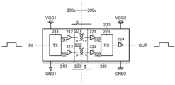
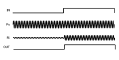
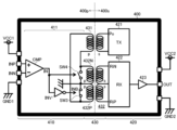
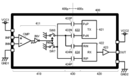
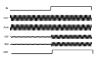
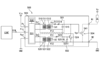
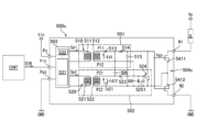
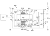
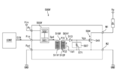
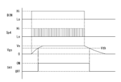
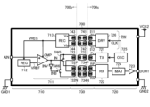
- ⁇ Signal transmission device (basic configuration)> 1 is a diagram showing the basic configuration of a signal transmission device.
- the signal transmission device 200 of this configuration example is a semiconductor integrated circuit device (so-called insulated gate driver IC) that transmits a pulse signal from the primary circuit system 200p to the secondary circuit system 200s while isolating the primary circuit system 200p (VCC1-GND1 system) from the secondary circuit system 200s (VCC2-GND2 system) and drives the gate of a switch element (not shown) provided in the secondary circuit system 200s.
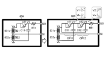
- the signal transmission device 200 is formed by sealing a controller chip 210, a driver chip 220, and a transformer chip 230 in a single package.
- the controller chip 210 is a semiconductor chip that operates by receiving a power supply voltage VCC1 (for example, up to 7 V based on GND1).
- the controller chip 210 includes, for example, a pulse transmission circuit 211 and buffers 212 and 213 integrated therein.
- the pulse transmission circuit 211 is a pulse generator that generates the transmission pulse signals S11 and S21 in response to the input pulse signal IN. More specifically, when the pulse transmission circuit 211 notifies that the input pulse signal IN is at a high level, it pulse drives the transmission pulse signal S11 (outputs a single or multiple transmission pulses), and when it notifies that the input pulse signal IN is at a low level, it pulse drives the transmission pulse signal S21. In other words, the pulse transmission circuit 211 pulse drives either the transmission pulse signal S11 or S21 in response to the logical level of the input pulse signal IN.
- the buffer 212 receives the transmission pulse signal S11 from the pulse transmission circuit 211 and pulse-drives the transformer chip 230 (specifically, the transformer 231).
- the buffer 213 receives the transmission pulse signal S21 from the pulse transmission circuit 211 and pulse-drives the transformer chip 230 (specifically, the transformer 232).
- the driver chip 220 is a semiconductor chip that operates by receiving a power supply voltage VCC2 (for example, up to 30 V based on GND2).
- the driver chip 220 includes, for example, buffers 221 and 222, a pulse receiving circuit 223, and a driver 224.
- the buffer 222 shapes the waveform of the received pulse signal S22 induced in the transformer chip 230 (specifically, the transformer 232) and outputs it to the pulse receiving circuit 223.
- the pulse receiving circuit 223 generates the output pulse signal OUT by driving the driver 224 in response to the received pulse signals S12 and S22 input via the buffers 221 and 222. More specifically, the pulse receiving circuit 223 drives the driver 224 so as to raise the output pulse signal OUT to a high level in response to the pulse drive of the received pulse signal S12, and to lower the output pulse signal OUT to a low level in response to the pulse drive of the received pulse signal S22. In other words, the pulse receiving circuit 223 switches the logical level of the output pulse signal OUT in response to the logical level of the input pulse signal IN.
- an RS flip-flop can be suitably used as the pulse receiving circuit 223.
- the driver 224 generates an output pulse signal OUT based on the drive control of the pulse receiving circuit 223.
- the transformer chip 230 uses transformers 231 and 232 to provide DC insulation between the controller chip 210 and the driver chip 220, and outputs the transmission pulse signals S11 and S21 input from the pulse transmission circuit 211 to the pulse reception circuit 223 as reception pulse signals S12 and S22, respectively.
- DC insulation means that the objects to be insulated are not connected by a conductor.
- the transformer 231 outputs a received pulse signal S12 from the secondary coil 231s in response to a transmitted pulse signal S11 input to the primary coil 231p.
- the transformer 232 outputs a received pulse signal S22 from the secondary coil 232s in response to a transmitted pulse signal S21 input to the primary coil 232p.
- the input pulse signal IN is separated into two transmission pulse signals S11 and S21 (corresponding to the rise signal and fall signal), and then transmitted from the primary circuit system 200p to the secondary circuit system 200s via the two transformers 231 and 232.
- the signal transmission device 200 of this configuration example has an independent transformer chip 230 equipped with only transformers 231 and 232, separate from the controller chip 210 and driver chip 220, and these three chips are sealed in a single package.
- the controller chip 210 and the driver chip 220 can both be formed using a general low to medium voltage process (withstands a few volts to a few tens of volts), eliminating the need to use a dedicated high voltage process (withstands a few kV), making it possible to reduce manufacturing costs.
- the signal transmission device 200 can be suitably used, for example, in a power supply device or a motor drive device for on-board equipment mounted in a vehicle.
- the above vehicles include not only engine vehicles, but also electric vehicles (BEVs [battery electric vehicles], HEVs [hybrid electric vehicles], PHEVs/PHVs (plug-in hybrid electric vehicles/plug-in hybrid vehicles), or xEVs such as FCEVs/FCVs (fuel cell electric vehicles/fuel cell vehicles)).
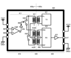
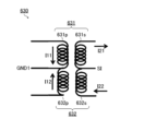
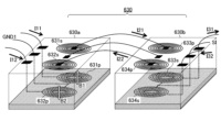
- FIG. 2 is a diagram showing the basic structure of the transformer chip 230.
- the transformer 231 includes a primary coil 231p and a secondary coil 231s that face each other in the vertical direction.
- the transformer 232 includes a primary coil 232p and a secondary coil 232s that face each other in the vertical direction.
- the primary coils 231p and 232p are both formed on the first wiring layer (lower layer) 230a of the transformer chip 230.
- the secondary coils 231s and 232s are both formed on the second wiring layer (upper layer in this figure) 230b of the transformer chip 230.
- the secondary coil 231s is disposed directly above the primary coil 231p and faces the primary coil 231p.
- the secondary coil 232s is disposed directly above the primary coil 232p and faces the primary coil 232p.
- the primary coil 231p is laid in a spiral shape starting from a first end connected to the internal terminal X21, surrounding the internal terminal X21 in a clockwise direction, and its second end corresponding to its end point is connected to the internal terminal X22.
- the primary coil 232p is laid in a spiral shape starting from a first end connected to the internal terminal X23, surrounding the internal terminal X23 in a counterclockwise direction, and its second end corresponding to its end point is connected to the internal terminal X22.
- the internal terminals X21, X22, and X23 are linearly arranged in the order shown.
- the internal terminal X21 is connected to the external terminal T21 of the second layer 230b via the conductive wiring Y21 and via Z21.
- the internal terminal X22 is connected to the external terminal T22 of the second layer 230b via the conductive wiring Y22 and via Z22.
- the internal terminal X23 is connected to the external terminal T23 of the second layer 230b via the conductive wiring Y23 and via Z23.
- the external terminals T21 to T23 are arranged in a straight line and are used for wire bonding with the controller chip 210.
- the secondary coil 231s is laid in a spiral shape starting from a first end connected to the external terminal T24, surrounding the external terminal T24 in a counterclockwise direction, and its second end corresponding to its end point is connected to the external terminal T25.
- the secondary coil 232s is laid in a spiral shape starting from a first end connected to the external terminal T26, surrounding the external terminal T26 in a clockwise direction, and its second end corresponding to its end point is connected to the external terminal T25.
- the external terminals T24, T25, and T26 are arranged linearly in the order shown in the figure, and are used for wire bonding with the driver chip 220.
- Secondary coils 231s and 232s are AC-connected to primary coils 231p and 232p by magnetic coupling, and are DC-insulated from primary coils 231p and 232p, respectively. That is, driver chip 220 is AC-connected to controller chip 210 via transformer chip 230, and is DC-insulated from controller chip 210 by transformer chip 230.
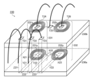
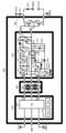
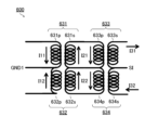
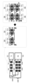
- FIG. 3 is a perspective view showing a semiconductor device 5 used as a two-channel transformer chip.
- FIG. 4 is a plan view of the semiconductor device 5 shown in FIG. 3.
- FIG. 5 is a plan view showing a layer in which a low-potential coil 22 (corresponding to a primary coil of a transformer) is formed in the semiconductor device 5 shown in FIG. 3.
- FIG. 6 is a plan view showing a layer in which a high-potential coil 23 (corresponding to a secondary coil of a transformer) is formed in the semiconductor device 5 shown in FIG. 3.
- FIG. 7 is a cross-sectional view taken along line VIII-VIII shown in FIG. 6.
- FIG. 8 is an enlarged view of region XIII shown in FIG. 7, showing an isolation structure 130.
- the semiconductor device 5 includes a semiconductor chip 41 having a rectangular parallelepiped shape.
- the semiconductor chip 41 includes at least one of silicon, a wide band gap semiconductor, and a compound semiconductor.
- a wide bandgap semiconductor is made of a semiconductor whose bandgap exceeds that of silicon (approximately 1.12 eV).
- the bandgap of a wide bandgap semiconductor is preferably 2.0 eV or more.
- the wide bandgap semiconductor may be SiC (silicon carbide).
- the compound semiconductor may be a III-V compound semiconductor.
- the compound semiconductor may include at least one of AlN (aluminum nitride), InN (indium nitride), GaN (gallium nitride), and GaAs (gallium arsenide).
- the semiconductor chip 41 includes a semiconductor substrate made of silicon.
- the semiconductor chip 41 may be an epitaxial substrate having a layered structure including a semiconductor substrate made of silicon and an epitaxial layer made of silicon.
- the conductivity type of the semiconductor substrate may be n-type or p-type.
- the epitaxial layer may be n-type or p-type.
- the semiconductor chip 41 has a first main surface 42 on one side, a second main surface 43 on the other side, and chip sidewalls 44A-44D connecting the first main surface 42 and the second main surface 43.
- the first main surface 42 and the second main surface 43 are formed in a quadrangular shape (rectangular in this embodiment) when viewed in a plan view from their normal direction Z (hereinafter simply referred to as "plan view").
- the chip sidewalls 44A to 44D include a first chip sidewall 44A, a second chip sidewall 44B, a third chip sidewall 44C, and a fourth chip sidewall 44D.
- the first chip sidewall 44A and the second chip sidewall 44B form the long sides of the semiconductor chip 41.
- the first chip sidewall 44A and the second chip sidewall 44B extend along the first direction X and face the second direction Y.
- the third chip sidewall 44C and the fourth chip sidewall 44D form the short sides of the semiconductor chip 41.
- the third chip sidewall 44C and the fourth chip sidewall 44D extend in the second direction Y and face the first direction X.
- the chip sidewalls 44A to 44D are made of ground surfaces.
- the semiconductor device 5 further includes an insulating layer 51 formed on the first main surface 42 of the semiconductor chip 41.
- the insulating layer 51 has an insulating main surface 52 and insulating side walls 53A-53D.
- the insulating main surface 52 is formed in a quadrangular shape (rectangular in this embodiment) that matches the first main surface 42 in a plan view.
- the insulating main surface 52 extends parallel to the first main surface 42.
- the insulating sidewalls 53A to 53D include a first insulating sidewall 53A, a second insulating sidewall 53B, a third insulating sidewall 53C, and a fourth insulating sidewall 53D.
- the insulating sidewalls 53A to 53D extend from the periphery of the insulating main surface 52 toward the semiconductor chip 41 and are continuous with the chip sidewalls 44A to 44D. Specifically, the insulating sidewalls 53A to 53D are formed flush with the chip sidewalls 44A to 44D.
- the insulating sidewalls 53A to 53D form a ground surface that is flush with the chip sidewalls 44A to 44D.
- the insulating layer 51 is made of a multi-layer insulating laminate structure including a bottom insulating layer 55, a top insulating layer 56, and a plurality of (11 in this embodiment) interlayer insulating layers 57.
- the bottom insulating layer 55 is an insulating layer that directly covers the first main surface 42.
- the top insulating layer 56 is an insulating layer that forms the insulating main surface 52.
- the plurality of interlayer insulating layers 57 are insulating layers interposed between the bottom insulating layer 55 and the top insulating layer 56.
- the bottom insulating layer 55 has a single-layer structure including silicon oxide.
- the top insulating layer 56 has a single-layer structure including silicon oxide.
- the thickness of the bottom insulating layer 55 and the top insulating layer 56 may each be 1 ⁇ m or more and 3 ⁇ m or less (for example, about 2 ⁇ m).
- the multiple interlayer insulating layers 57 each have a stacked structure including a first insulating layer 58 on the bottom insulating layer 55 side and a second insulating layer 59 on the top insulating layer 56 side.
- the first insulating layer 58 may include silicon nitride.
- the first insulating layer 58 is formed as an etching stopper layer for the second insulating layer 59.
- the thickness of the first insulating layer 58 may be 0.1 ⁇ m or more and 1 ⁇ m or less (for example, about 0.3 ⁇ m).
- the second insulating layer 59 is formed on the first insulating layer 58. It contains an insulating material different from that of the first insulating layer 58.
- the second insulating layer 59 may contain silicon oxide.
- the thickness of the second insulating layer 59 may be 1 ⁇ m or more and 3 ⁇ m or less (for example, about 2 ⁇ m). It is preferable that the thickness of the second insulating layer 59 exceeds the thickness of the first insulating layer 58.
- the total thickness DT of the insulating layers 51 may be 5 ⁇ m or more and 50 ⁇ m or less.
- the total thickness DT of the insulating layers 51 and the number of layers of the interlayer insulating layers 57 are arbitrary and are adjusted according to the dielectric strength voltage (dielectric breakdown resistance) to be achieved.
- the insulating materials of the bottom insulating layer 55, the top insulating layer 56 and the interlayer insulating layer 57 are arbitrary and are not limited to a specific insulating material.
- the semiconductor device 5 includes a first functional device 45 formed in an insulating layer 51.
- the first functional device 45 includes one or more (in this embodiment, multiple) transformers 21 (corresponding to the aforementioned transformer).
- the semiconductor device 5 is a multi-channel device including multiple transformers 21.
- the multiple transformers 21 are formed in the inner part of the insulating layer 51 at intervals from the insulating side walls 53A-53D.
- the multiple transformers 21 are formed at intervals in the first direction X.
- the multiple transformers 21 specifically include a first transformer 21A, a second transformer 21B, a third transformer 21C, and a fourth transformer 21D, which are formed in this order from the insulating side wall 53C side to the insulating side wall 53D side in a plan view.
- the multiple transformers 21A to 21D each have a similar structure.
- the structure of the first transformer 21A will be described as an example.
- the structures of the second transformer 21B, third transformer 21C, and fourth transformer 21D will be omitted as the description of the structure of the first transformer 21A applies mutatis mutandis.
- the first transformer 21A includes a low-potential coil 22 and a high-potential coil 23.
- the low-potential coil 22 is formed in an insulating layer 51.
- the high-potential coil 23 is formed in the insulating layer 51 so as to face the low-potential coil 22 in the normal direction Z.
- the low-potential coil 22 and the high-potential coil 23 are formed in a region sandwiched between the bottom insulating layer 55 and the top insulating layer 56 (i.e., multiple interlayer insulating layers 57).
- the low-potential coil 22 is formed on the bottom insulating layer 55 (semiconductor chip 41) side within the insulating layer 51, and the high-potential coil 23 is formed on the top insulating layer 56 (insulating main surface 52) side of the low-potential coil 22 within the insulating layer 51.
- the high-potential coil 23 faces the semiconductor chip 41 with the low-potential coil 22 in between.
- the low-potential coil 22 and the high-potential coil 23 may be positioned at any location. Furthermore, it is sufficient that the high-potential coil 23 faces the low-potential coil 22 with one or more interlayer insulating layers 57 in between.
- the distance between the low potential coil 22 and the high potential coil 23 (i.e., the number of layers of the interlayer insulating layer 57) is adjusted appropriately according to the dielectric strength and electric field strength between the low potential coil 22 and the high potential coil 23.
- the low potential coil 22 is formed in the third interlayer insulating layer 57 counting from the bottom insulating layer 55 side.
- the high potential coil 23 is formed in the first interlayer insulating layer 57 counting from the top insulating layer 56 side.
- the low-potential coil 22 is embedded in the interlayer insulating layer 57, penetrating the first insulating layer 58 and the second insulating layer 59.
- the low-potential coil 22 includes a first inner end 24, a first outer end 25, and a first spiral portion 26 wound in a spiral shape between the first inner end 24 and the first outer end 25.
- the first spiral portion 26 is wound in a spiral shape that extends in an elliptical shape (oval shape) in a plan view.
- the portion that forms the innermost periphery of the first spiral portion 26 defines a first inner region 66 that is elliptical in a plan view.
- the number of turns of the first spiral portion 26 may be 5 or more and 30 or less.
- the width of the first spiral portion 26 may be 0.1 ⁇ m or more and 5 ⁇ m or less.
- the width of the first spiral portion 26 is preferably 1 ⁇ m or more and 3 ⁇ m or less.
- the width of the first spiral portion 26 is defined by the width in a direction perpendicular to the spiral direction.
- the first winding pitch of the first spiral portion 26 may be 0.1 ⁇ m or more and 5 ⁇ m or less.
- the first winding pitch is preferably 1 ⁇ m or more and 3 ⁇ m or less.
- the first winding pitch is defined by the distance between two adjacent portions of the first spiral portion 26 in a direction perpendicular to the spiral direction.
- the winding shape of the first spiral portion 26 and the planar shape of the first inner region 66 are arbitrary and are not limited to the form shown in FIG. 5, etc.
- the first spiral portion 26 may be wound in a polygonal shape, such as a triangular shape or a rectangular shape, or in a circular shape in a planar view.
- the first inner region 66 may be partitioned into a polygonal shape, such as a triangular shape or a rectangular shape, or in a circular shape in a planar view, depending on the winding shape of the first spiral portion 26.
- the low potential coil 22 may include at least one of titanium, titanium nitride, copper, aluminum, and tungsten.
- the low potential coil 22 may have a laminated structure including a barrier layer and a main body layer.
- the barrier layer defines a recess space in the interlayer insulating layer 57.
- the barrier layer may include at least one of titanium and titanium nitride.
- the main body layer may include at least one of copper, aluminum, and tungsten.
- the high-potential coil 23 is embedded in the interlayer insulating layer 57, penetrating the first insulating layer 58 and the second insulating layer 59.
- the high-potential coil 23 includes a second inner end 27, a second outer end 28, and a second spiral portion 29 wound in a spiral shape between the second inner end 27 and the second outer end 28.
- the second spiral portion 29 is wound in a spiral shape extending in an elliptical shape (oval shape) in a planar view.
- the portion forming the innermost periphery of the second spiral portion 29 defines a second inner region 67 that is elliptical in a planar view.
- the second inner region 67 of the second spiral portion 29 faces the first inner region 66 of the first spiral portion 26 in the normal direction Z.
- the number of turns of the second spiral portion 29 may be 5 or more and 30 or less.
- the number of turns of the second spiral portion 29 relative to the number of turns of the first spiral portion 26 is adjusted according to the voltage value to be boosted. It is preferable that the number of turns of the second spiral portion 29 exceeds the number of turns of the first spiral portion 26.
- the number of turns of the second spiral portion 29 may be less than the number of turns of the first spiral portion 26, or may be equal to the number of turns of the first spiral portion 26.
- the width of the second spiral portion 29 may be 0.1 ⁇ m or more and 5 ⁇ m or less.
- the width of the second spiral portion 29 is preferably 1 ⁇ m or more and 3 ⁇ m or less.
- the width of the second spiral portion 29 is defined by the width in a direction perpendicular to the spiral direction.
- the width of the second spiral portion 29 is preferably equal to the width of the first spiral portion 26.
- the second winding pitch of the second spiral portion 29 may be 0.1 ⁇ m or more and 5 ⁇ m or less.
- the second winding pitch is preferably 1 ⁇ m or more and 3 ⁇ m or less.
- the second winding pitch is defined by the distance between two adjacent portions of the second spiral portion 29 in a direction perpendicular to the spiral direction.
- the second winding pitch is preferably equal to the first winding pitch of the first spiral portion 26.
- the winding shape of the second spiral portion 29 and the planar shape of the second inner region 67 are arbitrary and are not limited to the form shown in FIG. 6, etc.
- the second spiral portion 29 may be wound in a polygonal shape, such as a triangular shape or a rectangular shape, or in a circular shape in a planar view.
- the second inner region 67 may be partitioned into a polygonal shape, such as a triangular shape or a rectangular shape, or in a circular shape in a planar view, depending on the winding shape of the second spiral portion 29.
- the high-potential coil 23 is preferably formed from the same conductive material as the low-potential coil 22.
- the high-potential coil 23 preferably includes a barrier layer and a main body layer, similar to the low-potential coil 22.
- the semiconductor device 5 includes a plurality (12 in this figure) of low potential terminals 11 and a plurality (12 in this figure) of high potential terminals 12.
- the plurality of low potential terminals 11 are each electrically connected to the low potential coils 22 of the corresponding transformers 21A to 21D.
- the plurality of high potential terminals 12 are each electrically connected to the high potential coils 23 of the corresponding transformers 21A to 21D.
- the low-potential terminals 11 are formed on the insulating main surface 52 of the insulating layer 51. Specifically, the low-potential terminals 11 are formed in an area on the insulating sidewall 53B side at intervals in the second direction Y from the transformers 21A-21D, and are arranged at intervals in the first direction X.
- the low potential terminals 11 include a first low potential terminal 11A, a second low potential terminal 11B, a third low potential terminal 11C, a fourth low potential terminal 11D, a fifth low potential terminal 11E, and a sixth low potential terminal 11F.
- two of each of the low potential terminals 11A to 11F are formed.
- the number of low potential terminals 11A to 11F is arbitrary.
- the first low potential terminal 11A faces the first transformer 21A in the second direction Y in a plan view.
- the second low potential terminal 11B faces the second transformer 21B in the second direction Y in a plan view.
- the third low potential terminal 11C faces the third transformer 21C in the second direction Y in a plan view.
- the fourth low potential terminal 11D faces the fourth transformer 21D in the second direction Y in a plan view.
- the fifth low potential terminal 11E is formed in the area between the first low potential terminal 11A and the second low potential terminal 11B in a plan view.
- the sixth low potential terminal 11F is formed in the area between the third low potential terminal 11C and the fourth low potential terminal 11D in a plan view.
- the first low potential terminal 11A is electrically connected to the first inner end 24 of the first transformer 21A (low potential coil 22).
- the second low potential terminal 11B is electrically connected to the first inner end 24 of the second transformer 21B (low potential coil 22).
- the third low potential terminal 11C is electrically connected to the first inner end 24 of the third transformer 21C (low potential coil 22).
- the fourth low potential terminal 11D is electrically connected to the first inner end 24 of the fourth transformer 21D (low potential coil 22).
- the fifth low potential terminal 11E is electrically connected to the first outer end 25 of the first transformer 21A (low potential coil 22) and the first outer end 25 of the second transformer 21B (low potential coil 22).
- the sixth low potential terminal 11F is electrically connected to the first outer end 25 of the third transformer 21C (low potential coil 22) and the first outer end 25 of the fourth transformer 21D (low potential coil 22).
- the multiple high potential terminals 12 are formed on the insulating main surface 52 of the insulating layer 51 at intervals from the multiple low potential terminals 11. Specifically, the multiple high potential terminals 12 are formed in the area on the insulating side wall 53A side at intervals from the multiple low potential terminals 11 in the second direction Y, and are arranged at intervals in the first direction X.
- the multiple high potential terminals 12 are each formed in an area close to the corresponding transformer 21A-21D in a planar view.
- the high potential terminals 12 being close to the transformers 21A-21D means that the distance between the high potential terminal 12 and the transformer 21 in a planar view is less than the distance between the low potential terminal 11 and the high potential terminal 12.
- the multiple high potential terminals 12 are formed at intervals along the first direction X so as to face the multiple transformers 21A to 21D along the first direction X in a plan view. More specifically, the multiple high potential terminals 12 are formed at intervals along the first direction X so as to be located in the second inner region 67 of the high potential coil 23 and in the region between adjacent high potential coils 23 in a plan view. As a result, the multiple high potential terminals 12 are arranged in a row with the multiple transformers 21A to 21D in the first direction X in a plan view.
- the multiple high potential terminals 12 include a first high potential terminal 12A, a second high potential terminal 12B, a third high potential terminal 12C, a fourth high potential terminal 12D, a fifth high potential terminal 12E, and a sixth high potential terminal 12F.
- a first high potential terminal 12A a second high potential terminal 12B
- a third high potential terminal 12C a third high potential terminal 12C
- a fourth high potential terminal 12D a fifth high potential terminal 12E
- a sixth high potential terminal 12F a sixth high potential terminal 12F.
- two of each of the multiple high potential terminals 12A to 12F are formed.
- the number of multiple high potential terminals 12A to 12F is arbitrary.
- the first high potential terminal 12A is formed in the second inner region 67 of the first transformer 21A (high potential coil 23) in a plan view.
- the second high potential terminal 12B is formed in the second inner region 67 of the second transformer 21B (high potential coil 23) in a plan view.
- the third high potential terminal 12C is formed in the second inner region 67 of the third transformer 21C (high potential coil 23) in a plan view.
- the fourth high potential terminal 12D is formed in the second inner region 67 of the fourth transformer 21D (high potential coil 23) in a plan view.
- the fifth high potential terminal 12E is formed in the region between the first transformer 21A and the second transformer 21B in a plan view.
- the sixth high potential terminal 12F is formed in the region between the third transformer 21C and the fourth transformer 21D in a plan view.
- the first high potential terminal 12A is electrically connected to the second inner end 27 of the first transformer 21A (high potential coil 23).
- the second high potential terminal 12B is electrically connected to the second inner end 27 of the second transformer 21B (high potential coil 23).
- the third high potential terminal 12C is electrically connected to the second inner end 27 of the third transformer 21C (high potential coil 23).
- the fourth high potential terminal 12D is electrically connected to the second inner end 27 of the fourth transformer 21D (high potential coil 23).
- the fifth high potential terminal 12E is electrically connected to the second outer end 28 of the first transformer 21A (high potential coil 23) and the second outer end 28 of the second transformer 21B (high potential coil 23).
- the sixth high potential terminal 12F is electrically connected to the second outer end 28 of the third transformer 21C (high potential coil 23) and the second outer end 28 of the fourth transformer 21D (high potential coil 23).
- the semiconductor device 5 includes a first low potential wiring 31, a second low potential wiring 32, a first high potential wiring 33, and a second high potential wiring 34, each formed in an insulating layer 51.
- a plurality of first low potential wirings 31, a plurality of second low potential wirings 32, a plurality of first high potential wirings 33, and a plurality of second high potential wirings 34 are formed.
- the first low-potential wiring 31 and the second low-potential wiring 32 fix the low-potential coil 22 of the first transformer 21A and the low-potential coil 22 of the second transformer 21B to the same potential.
- the first low-potential wiring 31 and the second low-potential wiring 32 also fix the low-potential coil 22 of the third transformer 21C and the low-potential coil 22 of the fourth transformer 21D to the same potential.
- the first low-potential wiring 31 and the second low-potential wiring 32 fix all the low-potential coils 22 of the transformers 21A to 21D to the same potential.
- the first high-potential wiring 33 and the second high-potential wiring 34 fix the high-potential coil 23 of the first transformer 21A and the high-potential coil 23 of the second transformer 21B to the same potential.
- the first high-potential wiring 33 and the second high-potential wiring 34 also fix the high-potential coil 23 of the third transformer 21C and the high-potential coil 23 of the fourth transformer 21D to the same potential.
- the first high-potential wiring 33 and the second high-potential wiring 34 fix all the high-potential coils 23 of the transformers 21A to 21D to the same potential.
- the multiple first low potential wirings 31 are electrically connected to the corresponding low potential terminals 11A to 11D and the first inner ends 24 of the corresponding transformers 21A to 21D (low potential coils 22).
- the multiple first low potential wirings 31 have the same structure.
- the structure of the first low potential wiring 31 connected to the first low potential terminal 11A and the first transformer 21A will be described as an example.
- the structure of the other first low potential wirings 31 will be omitted, as the description of the structure of the first low potential wiring 31 connected to the first transformer 21A applies mutatis mutandis.
- the first low-potential wiring 31 includes a through wiring 71, a low-potential connection wiring 72, a lead-out wiring 73, a first connection plug electrode 74, a second connection plug electrode 75, one or more (in this embodiment, multiple) pad plug electrodes 76, and one or more (in this embodiment, multiple) substrate plug electrodes 77.
- the through wiring 71, the low-potential connection wiring 72, the draw-out wiring 73, the first connection plug electrode 74, the second connection plug electrode 75, the pad plug electrode 76, and the substrate plug electrode 77 are preferably each formed from the same conductive material as the low-potential coil 22, etc.
- the through wiring 71, the low-potential connection wiring 72, the draw-out wiring 73, the first connection plug electrode 74, the second connection plug electrode 75, the pad plug electrode 76, and the substrate plug electrode 77 preferably each include a barrier layer and a main body layer, similar to the low-potential coil 22, etc.
- the through wiring 71 penetrates the multiple interlayer insulating layers 57 in the insulating layer 51 and extends in a columnar shape extending along the normal direction Z.
- the through wiring 71 is formed in the region between the bottom insulating layer 55 and the top insulating layer 56 in the insulating layer 51.
- the through wiring 71 has an upper end on the top insulating layer 56 side and a lower end on the bottom insulating layer 55 side.
- the upper end of the through wiring 71 is formed in the same interlayer insulating layer 57 as the high potential coil 23 and is covered by the top insulating layer 56.
- the lower end of the through wiring 71 is formed in the same interlayer insulating layer 57 as the low potential coil 22.
- the through wiring 71 includes a first electrode layer 78, a second electrode layer 79, and a plurality of wiring plug electrodes 80.
- the first electrode layer 78, the second electrode layer 79, and the wiring plug electrodes 80 are each formed from the same conductive material as the low potential coil 22, etc.
- the first electrode layer 78, the second electrode layer 79, and the wiring plug electrodes 80 each include a barrier layer and a main body layer, similar to the low potential coil 22, etc.
- the first electrode layer 78 forms the upper end of the through wiring 71.
- the second electrode layer 79 forms the lower end of the through wiring 71.
- the first electrode layer 78 is formed in an island shape and faces the low potential terminal 11 (first low potential terminal 11A) in the normal direction Z.
- the second electrode layer 79 is formed in an island shape and faces the first electrode layer 78 in the normal direction Z.
- the multiple wiring plug electrodes 80 are embedded in multiple interlayer insulating layers 57 located in the region between the first electrode layer 78 and the second electrode layer 79.
- the multiple wiring plug electrodes 80 are stacked from the bottom insulating layer 55 toward the top insulating layer 56 so as to be electrically connected to each other, and electrically connect the first electrode layer 78 and the second electrode layer 79.
- the multiple wiring plug electrodes 80 each have a planar area less than the planar area of the first electrode layer 78 and the planar area of the second electrode layer 79.
- the number of layers of the multiple wiring plug electrodes 80 matches the number of layers of the multiple interlayer insulating layers 57. In this embodiment, six wiring plug electrodes 80 are embedded in each interlayer insulating layer 57, but the number of wiring plug electrodes 80 embedded in each interlayer insulating layer 57 is arbitrary. Of course, one or more wiring plug electrodes 80 may be formed penetrating the multiple interlayer insulating layers 57.
- the low-potential connection wiring 72 is formed in the first inner region 66 of the first transformer 21A (low-potential coil 22) in the same interlayer insulating layer 57 as the low-potential coil 22.
- the low-potential connection wiring 72 is formed in an island shape and faces the high-potential terminal 12 (first high-potential terminal 12A) in the normal direction Z. It is preferable that the low-potential connection wiring 72 has a planar area that exceeds the planar area of the wiring plug electrode 80.
- the low-potential connection wiring 72 is electrically connected to the first inner end 24 of the low-potential coil 22.
- the draw-out wiring 73 is formed in the interlayer insulating layer 57 in the region between the semiconductor chip 41 and the through wiring 71.
- the draw-out wiring 73 is formed in the first interlayer insulating layer 57 counting from the bottom insulating layer 55.
- the draw-out wiring 73 includes a first end on one side, a second end on the other side, and a wiring portion connecting the first end and the second end.
- the first end of the draw-out wiring 73 is located in the region between the semiconductor chip 41 and the lower end of the through wiring 71.
- the second end of the draw-out wiring 73 is located in the region between the semiconductor chip 41 and the low-potential connection wiring 72.
- the wiring portion extends along the first main surface 42 of the semiconductor chip 41 and extends in a band shape in the region between the first end and the second end.
- the first connection plug electrode 74 is formed in the interlayer insulating layer 57 in the region between the through wiring 71 and the draw-out wiring 73, and is electrically connected to first ends of the through wiring 71 and the draw-out wiring 73.
- the second connection plug electrode 75 is formed in the interlayer insulating layer 57 in the region between the low-potential connection wiring 72 and the draw-out wiring 73, and is electrically connected to second ends of the low-potential connection wiring 72 and the draw-out wiring 73.
- the multiple pad plug electrodes 76 are formed in the uppermost insulating layer 56 in a region between the low potential terminal 11 (first low potential terminal 11A) and the through wiring 71, and are electrically connected to the upper ends of the low potential terminal 11 and the through wiring 71, respectively.
- the multiple substrate plug electrodes 77 are formed in the lowermost insulating layer 55 in a region between the semiconductor chip 41 and the draw-out wiring 73. In this embodiment, the substrate plug electrodes 77 are formed in a region between the semiconductor chip 41 and the first ends of the draw-out wiring 73, and are electrically connected to the semiconductor chip 41 and the first ends of the draw-out wiring 73, respectively.
- the multiple first high potential wirings 33 are electrically connected to the corresponding high potential terminals 12A-12D and the second inner ends 27 of the corresponding transformers 21A-21D (high potential coils 23).
- the multiple first high potential wirings 33 each have a similar structure.
- the structure of the first high potential wiring 33 connected to the first high potential terminal 12A and the first transformer 21A will be described as an example.
- the structure of the other first high potential wirings 33 will be omitted, as the description of the structure of the first high potential wiring 33 connected to the first transformer 21A applies mutatis mutandis.
- the first high-potential wiring 33 includes a high-potential connection wiring 81 and one or more (in this embodiment, multiple) pad plug electrodes 82.
- the high-potential connection wiring 81 and the pad plug electrode 82 are preferably formed from the same conductive material as the low-potential coil 22, etc.
- the high-potential connection wiring 81 and the pad plug electrode 82 preferably include a barrier layer and a main body layer, similar to the low-potential coil 22, etc.
- the high-potential connection wiring 81 is formed in the second inner region 67 of the high-potential coil 23 in the same interlayer insulating layer 57 as the high-potential coil 23.
- the high-potential connection wiring 81 is formed in an island shape and faces the high-potential terminal 12 (first high-potential terminal 12A) in the normal direction Z.
- the high-potential connection wiring 81 is electrically connected to the second inner end 27 of the high-potential coil 23.
- the high-potential connection wiring 81 is formed at a distance from the low-potential connection wiring 72 in a plan view and does not face the low-potential connection wiring 72 in the normal direction Z. This increases the insulation distance between the low-potential connection wiring 72 and the high-potential connection wiring 81, and increases the dielectric strength of the insulating layer 51.
- the multiple pad plug electrodes 82 are formed in the uppermost insulating layer 56 in a region between the high potential terminal 12 (first high potential terminal 12A) and the high potential connection wiring 81, and are electrically connected to the high potential terminal 12 and the high potential connection wiring 81, respectively.
- the multiple pad plug electrodes 82 each have a planar area less than the planar area of the high potential connection wiring 81 in a plan view.
- the distance D1 between the low potential terminal 11 and the high potential terminal 12 is preferably greater than the distance D2 between the low potential coil 22 and the high potential coil 23 (D2 ⁇ D1).
- the distance D1 is preferably greater than the total thickness DT of the multiple interlayer insulating layers 57 (DT ⁇ D1).
- the ratio D2/D1 of the distance D2 to the distance D1 may be 0.01 or more and 0.1 or less.
- the distance D1 is preferably 100 ⁇ m or more and 500 ⁇ m or less.
- the distance D2 may be 1 ⁇ m or more and 50 ⁇ m or less.
- the distance D2 is preferably 5 ⁇ m or more and 25 ⁇ m or less.
- the values of the distance D1 and the distance D2 are arbitrary and are adjusted appropriately according to the dielectric strength voltage to be realized.
- the semiconductor device 5 includes a dummy pattern 85 embedded in the insulating layer 51 so as to be positioned around the transformers 21A to 21D in a plan view.
- the dummy pattern 85 is formed in a pattern (discontinuous pattern) different from the high potential coil 23 and the low potential coil 22, and is independent of the transformers 21A to 21D. In other words, the dummy pattern 85 does not function as a transformer 21A to 21D.
- the dummy pattern 85 is formed as a shield conductor layer that shields the electric field between the low potential coil 22 and the high potential coil 23 in the transformers 21A to 21D and suppresses electric field concentration on the high potential coil 23.
- the dummy pattern 85 is routed with a line density equal to the line density of the high potential coil 23 per unit area.
- the line density of the dummy pattern 85 being equal to the line density of the high potential coil 23 means that the line density of the dummy pattern 85 falls within a range of ⁇ 20% of the line density of the high potential coil 23.
- the depth position of the dummy pattern 85 inside the insulating layer 51 is arbitrary and is adjusted according to the electric field strength to be relaxed.
- the dummy pattern 85 is preferably formed in a region closer to the high potential coil 23 than to the low potential coil 22 in the normal direction Z. Note that the dummy pattern 85 being closer to the high potential coil 23 in the normal direction Z means that the distance between the dummy pattern 85 and the high potential coil 23 in the normal direction Z is less than the distance between the dummy pattern 85 and the low potential coil 22.
- the dummy pattern 85 is preferably formed in the same interlayer insulating layer 57 as the high-potential coil 23. In this case, electric field concentration on the high-potential coil 23 can be further appropriately suppressed.
- the dummy pattern 85 includes multiple dummy patterns with different electrical states.
- the dummy pattern 85 may include a high-potential dummy pattern.
- the depth position of the high-potential dummy pattern 86 inside the insulating layer 51 is arbitrary and is adjusted according to the electric field strength to be relaxed.
- the high-potential dummy pattern 86 is preferably formed in a region closer to the high-potential coil 23 than the low-potential coil 22 in the normal direction Z.
- the high-potential dummy pattern 86 being closer to the high-potential coil 23 in the normal direction Z means that the distance between the high-potential dummy pattern 86 and the high-potential coil 23 in the normal direction Z is less than the distance between the high-potential dummy pattern 86 and the low-potential coil 22.
- the dummy pattern 85 includes a floating dummy pattern formed in an electrically floating state within the insulating layer 51 so as to be positioned around the transformers 21A to 21D.
- the floating dummy pattern is routed in dense lines so as to partially cover and partially expose the area around the high-potential coil 23 in a plan view.
- the floating dummy pattern may be formed with ends or without ends.
- the depth position of the floating dummy pattern inside the insulating layer 51 is arbitrary and is adjusted according to the electric field strength to be mitigated.
- the number of floating lines is arbitrary and is adjusted according to the electric field to be mitigated.
- the floating dummy pattern may be composed of multiple floating lines.
- the semiconductor device 5 includes a second functional device 60 formed on the first main surface 42 of the semiconductor chip 41 in a device region 62.
- the second functional device 60 is formed using a surface portion of the first main surface 42 of the semiconductor chip 41 and/or a region above the first main surface 42 of the semiconductor chip 41, and is covered by an insulating layer 51 (lowest insulating layer 55).
- the second functional device 60 is shown in a simplified form by a dashed line drawn on the surface portion of the first main surface 42.
- the second functional device 60 is electrically connected to the low potential terminal 11 via a low potential wiring, and is electrically connected to the high potential terminal 12 via a high potential wiring.
- the low potential wiring has a structure similar to that of the first low potential wiring 31 (second low potential wiring 32), except that it is routed within the insulating layer 51 so as to be connected to the second functional device 60.
- the high potential wiring has a structure similar to that of the first high potential wiring 33 (second high potential wiring 34), except that it is routed within the insulating layer 51 so as to be connected to the second functional device 60.
- a specific description of the low potential wiring and high potential wiring related to the second functional device 60 will be omitted.
- the second functional device 60 may include at least one of a passive device, a semiconductor rectifier device, and a semiconductor switching device.
- the second functional device 60 may include a circuit network in which any two or more types of devices selected from the passive device, the semiconductor rectifier device, and the semiconductor switching device are selectively combined.
- the circuit network may form part or all of an integrated circuit.
- the passive device may include a semiconductor passive device.
- the passive device may include either or both of a resistor and a capacitor.
- the semiconductor rectifier device may include at least one of a pn junction diode, a PIN diode, a Zener diode, a Schottky barrier diode, and a fast recovery diode.
- the semiconductor switching device may include at least one of a BJT [Bipolar Junction Transistor], a MISFET [Metal Insulator Semiconductor Field Effect Transistor], an IGBT [Insulated Gate Bipolar Junction Transistor], and a JFET [Junction Field Effect Transistor].
- the semiconductor device 5 further includes a seal conductor 61 embedded in the insulating layer 51.
- the seal conductor 61 is embedded in the insulating layer 51 in a wall shape at a distance from the insulating side walls 53A to 53D in a plan view, and divides the insulating layer 51 into a device region 62 and an outer region 63.
- the seal conductor 61 prevents moisture and cracks from entering the device region 62 from the outer region 63.
- the device region 62 is an area including the first functional device 45 (multiple transformers 21), the second functional device 60, multiple low potential terminals 11, multiple high potential terminals 12, the first low potential wiring 31, the second low potential wiring 32, the first high potential wiring 33, the second high potential wiring 34, and the dummy pattern 85.
- the outer region 63 is an area outside the device region 62.
- the seal conductor 61 is electrically isolated from the device region 62. Specifically, the seal conductor 61 is electrically isolated from the first functional device 45 (multiple transformers 21), the second functional device 60, the multiple low potential terminals 11, the multiple high potential terminals 12, the first low potential wiring 31, the second low potential wiring 32, the first high potential wiring 33, the second high potential wiring 34, and the dummy pattern 85. More specifically, the seal conductor 61 is fixed in an electrically floating state. The seal conductor 61 does not form a current path leading to the device region 62.
- the seal conductor 61 is formed in a band shape along the insulating side walls 53 to 53D in a plan view.
- the seal conductor 61 is formed in a square ring shape (specifically, a rectangular ring shape) in a plan view.
- the seal conductor 61 defines a square-shaped (specifically, rectangular) device region 62 in a plan view.
- the seal conductor 61 also defines a square-shaped (specifically, rectangular) outer region 63 that surrounds the device region 62 in a plan view.
- the seal conductor 61 has an upper end on the insulating principal surface 52 side, a lower end on the semiconductor chip 41 side, and a wall extending in a wall shape between the upper end and the lower end.
- the upper end of the seal conductor 61 is formed at a distance from the insulating principal surface 52 to the semiconductor chip 41 side, and is located within the insulating layer 51.
- the upper end of the seal conductor 61 is covered by the uppermost insulating layer 56.
- the upper end of the seal conductor 61 may be covered by one or more interlayer insulating layers 57.
- the upper end of the seal conductor 61 may be exposed from the uppermost insulating layer 56.
- the lower end of the seal conductor 61 is formed at a distance from the semiconductor chip 41 toward the upper end side.
- the seal conductor 61 is embedded in the insulating layer 51 so as to be located on the semiconductor chip 41 side relative to the multiple low potential terminals 11 and multiple high potential terminals 12. Furthermore, the seal conductor 61 faces the first functional device 45 (multiple transformers 21), the first low potential wiring 31, the second low potential wiring 32, the first high potential wiring 33, the second high potential wiring 34, and the dummy pattern 85 in the insulating layer 51 in a direction parallel to the insulating principal surface 52.
- the seal conductor 61 may face a part of the second functional device 60 in the insulating layer 51 in a direction parallel to the insulating principal surface 52.
- the seal conductor 61 includes a plurality of seal plug conductors 64 and one or more (in this embodiment, multiple) seal via conductors 65.
- the number of seal via conductors 65 is arbitrary.
- the uppermost seal plug conductor 64 among the plurality of seal plug conductors 64 forms the upper end of the seal conductor 61.
- the plurality of seal via conductors 65 each form the lower end of the seal conductor 61.
- the seal plug conductor 64 and the seal via conductor 65 are preferably formed from the same conductive material as the low potential coil 22. In other words, the seal plug conductor 64 and the seal via conductor 65 preferably include a barrier layer and a main body layer, similar to the low potential coil 22, etc.
- the multiple seal plug conductors 64 are embedded in the multiple interlayer insulating layers 57, and are each formed in a square ring shape (specifically, a rectangular ring shape) surrounding the device region 62 in a planar view.
- the multiple seal plug conductors 64 are stacked from the bottom insulating layer 55 to the top insulating layer 56 so as to be connected to each other.
- the number of stacked layers of the multiple seal plug conductors 64 matches the number of stacked layers of the multiple interlayer insulating layers 57.
- one or more seal plug conductors 64 may be formed penetrating the multiple interlayer insulating layers 57.
- a single annular seal conductor 61 is formed by an assembly of multiple seal plug conductors 64, it is not necessary for all of the multiple seal plug conductors 64 to be formed in an annular shape.
- at least one of the multiple seal plug conductors 64 may be formed with ends.
- at least one of the multiple seal plug conductors 64 may be divided into multiple strip-shaped portions with ends.
- the multiple seal plug conductors 64 are formed in an endless (annular) shape.
- the multiple seal via conductors 65 are each formed in the area between the semiconductor chip 41 and the seal plug conductor 64 in the bottom insulating layer 55.
- the multiple seal via conductors 65 are formed at a distance from the semiconductor chip 41 and are connected to the seal plug conductor 64.
- the multiple seal via conductors 65 have a planar area less than the planar area of the seal plug conductor 64.
- the single seal via conductor 65 may have a planar area equal to or greater than the planar area of the seal plug conductor 64.
- the width of the sealing conductor 61 may be 0.1 ⁇ m or more and 10 ⁇ m or less.
- the width of the sealing conductor 61 is preferably 1 ⁇ m or more and 5 ⁇ m or less.
- the width of the sealing conductor 61 is defined by the width in a direction perpendicular to the direction in which the sealing conductor 61 extends.
- the semiconductor device 5 further includes an isolation structure 130 that is interposed between the semiconductor chip 41 and the seal conductor 61 and electrically isolates the seal conductor 61 from the semiconductor chip 41.
- the isolation structure 130 preferably includes an insulator.
- the isolation structure 130 is made of a field insulating film 131 formed on the first main surface 42 of the semiconductor chip 41.
- the field insulating film 131 includes at least one of an oxide film (silicon oxide film) and a nitride film (silicon nitride film).
- the field insulating film 131 is preferably made of a LOCOS (local oxidation of silicon) film, which is an example of an oxide film formed by oxidizing the first main surface 42 of the semiconductor chip 41.
- the thickness of the field insulating film 131 is arbitrary as long as it can insulate the semiconductor chip 41 and the seal conductor 61.
- the thickness of the field insulating film 131 may be 0.1 ⁇ m or more and 5 ⁇ m or less.
- the isolation structure 130 is formed on the first main surface 42 of the semiconductor chip 41, and extends in a band shape along the seal conductor 61 in a planar view.
- the isolation structure 130 is formed in a square ring shape (specifically, a rectangular ring shape) in a planar view.
- the isolation structure 130 has a connection portion 132 to which the lower end portion (seal via conductor 65) of the seal conductor 61 is connected.
- the connection portion 132 may form an anchor portion in which the lower end portion (seal via conductor 65) of the seal conductor 61 is embedded toward the semiconductor chip 41.
- the connection portion 132 may be formed flush with the main surface of the isolation structure 130.
- the separation structure 130 includes an inner end 130A on the device region 62 side, an outer end 130B on the outer region 63 side, and a main body 130C between the inner end 130A and the outer end 130B.
- the inner end 130A defines the region in which the second functional device 60 is formed (i.e., the device region 62) in a plan view.
- the inner end 130A may be formed integrally with an insulating film (not shown) formed on the first main surface 42 of the semiconductor chip 41.
- the outer end 130B is exposed from the chip sidewalls 44A to 44D of the semiconductor chip 41 and is continuous with the chip sidewalls 44A to 44D of the semiconductor chip 41. More specifically, the outer end 130B is formed flush with the chip sidewalls 44A to 44D of the semiconductor chip 41. The outer end 130B forms a flush ground surface between the chip sidewalls 44A to 44D of the semiconductor chip 41 and the insulating sidewalls 53A to 53D of the insulating layer 51. Of course, in other embodiments, the outer end 130B may be formed in the first main surface 42 at a distance from the chip sidewalls 44A to 44D.
- the main body 130C has a flat surface that extends approximately parallel to the first main surface 42 of the semiconductor chip 41.
- the main body 130C has a connection portion 132 to which the lower end portion (seal via conductor 65) of the seal conductor 61 is connected.
- the connection portion 132 is formed in a portion of the main body 130C that is spaced apart from the inner end portion 130A and the outer end portion 130B.
- the isolation structure 130 can take various forms in addition to the field insulating film 131.
- the semiconductor device 5 further includes an inorganic insulating layer 140 formed on the insulating principal surface 52 of the insulating layer 51 so as to cover the seal conductor 61.
- the inorganic insulating layer 140 may be referred to as a passivation layer.
- the inorganic insulating layer 140 protects the insulating layer 51 and the semiconductor chip 41 from above the insulating principal surface 52.
- the inorganic insulating layer 140 has a laminated structure including a first inorganic insulating layer 141 and a second inorganic insulating layer 142.
- the first inorganic insulating layer 141 may include silicon oxide.
- the first inorganic insulating layer 141 preferably includes USG (undoped silicate glass), which is silicon oxide without added impurities.
- the thickness of the first inorganic insulating layer 141 may be 50 nm or more and 5000 nm or less.
- the second inorganic insulating layer 142 may include silicon nitride.
- the thickness of the second inorganic insulating layer 142 may be 500 nm or more and 5000 nm or less.
- the breakdown voltage (V/cm) of the USG exceeds the breakdown voltage (V/cm) of silicon nitride. Therefore, when thickening the inorganic insulating layer 140, it is preferable to form the first inorganic insulating layer 141 thicker than the second inorganic insulating layer 142.
- the first inorganic insulating layer 141 may contain at least one of BPSG (boron doped phosphor silicate glass) and PSG (phosphorus silicate glass), which are examples of silicon oxide. However, in this case, since impurities (boron or phosphorus) are contained in the silicon oxide, it is particularly preferable to form the first inorganic insulating layer 141 made of USG in order to increase the dielectric strength on the high-potential coil 23.
- the inorganic insulating layer 140 may have a single-layer structure made of either the first inorganic insulating layer 141 or the second inorganic insulating layer 142.
- the inorganic insulating layer 140 covers the entire area of the sealing conductor 61, and has a plurality of low potential pad openings 143 and a plurality of high potential pad openings 144 formed in the area outside the sealing conductor 61.
- the plurality of low potential pad openings 143 expose the plurality of low potential terminals 11, respectively.
- the plurality of high potential pad openings 144 expose the plurality of high potential terminals 12, respectively.
- the inorganic insulating layer 140 may have an overlap portion that rides up on the peripheral portion of the low potential terminal 11.
- the inorganic insulating layer 140 may have an overlap portion that rides up on the peripheral portion of the high potential terminal 12.
- the semiconductor device 5 further includes an organic insulating layer 145 formed on the inorganic insulating layer 140.
- the organic insulating layer 145 may include a photosensitive resin.
- the organic insulating layer 145 may include at least one of polyimide, polyamide, and polybenzoxazole. In this embodiment, the organic insulating layer 145 includes polyimide.
- the thickness of the organic insulating layer 145 may be 1 ⁇ m or more and 50 ⁇ m or less.
- the thickness of the organic insulating layer 145 is preferably greater than the total thickness of the inorganic insulating layer 140. Furthermore, the total thickness of the inorganic insulating layer 140 and the organic insulating layer 145 is preferably greater than or equal to the distance D2 between the low potential coil 22 and the high potential coil 23. In this case, the total thickness of the inorganic insulating layer 140 is preferably greater than or equal to 2 ⁇ m and less than or equal to 10 ⁇ m. Furthermore, the thickness of the organic insulating layer 145 is preferably greater than or equal to 5 ⁇ m and less than or equal to 50 ⁇ m.
- These structures can suppress the thickening of the inorganic insulating layer 140 and the organic insulating layer 145, while at the same time, the laminated film of the inorganic insulating layer 140 and the organic insulating layer 145 can appropriately increase the dielectric strength voltage on the high potential coil 23.
- the organic insulating layer 145 includes a first portion 146 covering the region on the low potential side and a second portion 147 covering the region on the high potential side.
- the first portion 146 covers the seal conductor 61 with the inorganic insulating layer 140 in between.
- the first portion 146 has a plurality of low potential terminal openings 148 that expose a plurality of low potential terminals 11 (low potential pad openings 143) in the region outside the seal conductor 61.
- the first portion 146 may have an overlap portion that rises onto the periphery (overlap portion) of the low potential pad opening 143.
- the second portion 147 is formed at a distance from the first portion 146, exposing the inorganic insulating layer 140 between the second portion 147 and the first portion 146.
- the second portion 147 has a plurality of high potential terminal openings 149 that respectively expose a plurality of high potential terminals 12 (high potential pad openings 144).
- the second portion 147 may have an overlap portion that rises onto the periphery (overlap portion) of the high potential pad opening 144.
- the second portion 147 collectively covers the transformers 21A-21D and the dummy pattern 85. Specifically, the second portion 147 collectively covers the multiple high potential coils 23, the multiple high potential terminals 12, the first high potential dummy pattern 87, the second high potential dummy pattern 88, and the floating dummy pattern 121.
- the embodiments of the present invention can be implemented in further different forms.
- an example was described in which a first functional device 45 and a second functional device 60 were formed.
- a form having only the second functional device 60 without the first functional device 45 may also be adopted.
- the dummy pattern 85 may be removed.
- the second functional device 60 can achieve the same effects as those described in the first embodiment (excluding the effects associated with the dummy pattern 85).
- the second functional device 60 was formed.
- the second functional device 60 is not necessarily required and may be removed.
- the dummy pattern 85 was formed.
- the dummy pattern 85 is not necessarily required and may be removed.
- the first functional device 45 is a multi-channel type that includes multiple transformers 21.
- a first functional device 45 that is a single-channel type that includes a single transformer 21 may also be used.
- ⁇ Transformer arrangement> 9 is a plan view (top view) showing a schematic example of a transformer arrangement in a two-channel transformer chip 300 (corresponding to the semiconductor device 5 described above).
- the transformer chip 300 in this figure has a first transformer 301, a second transformer 302, a third transformer 303, a fourth transformer 304, a first guard ring 305, a second guard ring 306, pads a1 to a8, pads b1 to b8, pads c1 to c4, and pads d1 to d4.
- pads a1 and b1 are connected to one end of the secondary coil L1s forming the first transformer 301, and pads c1 and d1 are connected to the other end of the secondary coil L1s.
- Pads a2 and b2 are connected to one end of the secondary coil L2s forming the second transformer 302, and pads c1 and d1 are connected to the other end of the secondary coil L2s.
- pads a3 and b3 are connected to one end of the secondary coil L3s forming the third transformer 303, and pads c2 and d2 are connected to the other end of the secondary coil L3s.
- Pads a4 and b4 are connected to one end of the secondary coil L4s forming the fourth transformer 304, and pads c2 and d2 are connected to the other end of the secondary coil L4s.
- the primary coil forming the first transformer 301, the primary coil forming the second transformer 302, the primary coil forming the third transformer 303, and the primary coil forming the fourth transformer 304 are not shown in this diagram.
- the primary coils basically have the same configuration as the secondary coils L1s to L4s, and are arranged directly below each of the secondary coils L1s to L4s, facing the secondary coils L1s to L4s, respectively.
- pads a5 and b5 are connected to one end of the primary coil forming the first transformer 301, and pads c3 and d3 are connected to the other end of the primary coil. Also, pads a6 and b6 are connected to one end of the primary coil forming the second transformer 302, and pads c3 and d3 are connected to the other end of the primary coil.
- pads a7 and b7 are connected to one end of the primary coil forming the third transformer 303, and pads c4 and d4 are connected to the other end of the primary coil. Furthermore, pads a8 and b8 are connected to one end of the primary coil forming the fourth transformer 304, and pads c4 and d4 are connected to the other end of the primary coil.
- pads a5 to a8, pads b5 to b8, pads c3 and c4, and pads d3 and d4 are pulled out from the inside of the transformer chip 300 to the surface through vias (not shown).
- pads a1 to a8 correspond to first current supply pads
- pads b1 to b8 correspond to first voltage measurement pads
- pads c1 to c4 correspond to second current supply pads
- pads d1 to d4 correspond to second voltage measurement pads.
- the series resistance component of each coil can be accurately measured during the defective product inspection. This makes it possible to not only reject defective products where each coil has a break in the wire, but also to appropriately reject defective products where the resistance value of each coil is abnormal (for example, a short circuit between coils), which in turn makes it possible to prevent defective products from being released onto the market.
- the above-mentioned multiple pads can be used as a connection means with the primary side chip and the secondary side chip (for example, the aforementioned controller chip 210 and driver chip 220).
- pads a1 and b1, pads a2 and b2, pads a3 and b3, and pads a4 and b4 may be connected to the signal input or output terminals of the secondary chip, respectively.
- pads c1 and d1, and pads c2 and d2 may be connected to the common voltage application terminal (GND2) of the secondary chip, respectively.
- pads a5 and b5, pads a6 and b6, pads a7 and b7, and pads a8 and b8 may be connected to the signal input or output terminals of the primary chip, respectively.
- pads c3 and d3, and pads c4 and d4 may be connected to the common voltage application terminal (GND1) of the primary chip, respectively.
- the first transformer 301 to the fourth transformer 304 are arranged in a coupled manner according to the respective signal transmission directions.
- the first transformer 301 and the second transformer 302 which transmit signals from the primary chip to the secondary chip are arranged as a first pair by the first guard ring 305.
- the third transformer 303 and the fourth transformer 304, which transmit signals from the secondary chip to the primary chip are arranged as a second pair by the second guard ring 306.
- the reason for this coupling is to ensure a sufficient withstand voltage between the primary coil and the secondary coil when the primary coil and the secondary coil that respectively form the first transformer 301 to the fourth transformer 304 are stacked vertically on the substrate of the transformer chip 300.
- the first guard ring 305 and the second guard ring 306 are not necessarily essential components.
- the first guard ring 305 and the second guard ring 306 may be connected to a low impedance wiring such as a ground terminal via pads e1 and e2, respectively.
- pads c1 and d1 are shared between the secondary coil L1s and secondary coil L2s.
- Pads c2 and d2 are shared between the secondary coil L3s and secondary coil L4s.
- Pads c3 and d3 are shared between the primary coil L1p and primary coil L2p.
- Pads c4 and d4 are shared between the corresponding primary coils. This configuration makes it possible to reduce the number of pads and miniaturize the transformer chip 300.
- transformer arrangement in this diagram is merely one example, and the number, shape, and arrangement of the coils, as well as the arrangement of the pads, are optional.
- chip structure and transformer arrangement that have been explained so far can be applied to semiconductor devices in general that integrate coils on a semiconductor chip.
- a signal transmission device that transmits signals between a primary circuit system and a secondary circuit system while electrically isolating them is supplied with power from the power supplies of the primary circuit system and the secondary circuit system.
- the power supplies of the primary circuit system and the secondary circuit system each have sufficient current supply capacity.
- the side that transmits the signal e.g., the primary circuit system
- the power supply of the primary circuit system is unstable or insufficient, the signal transmission from the primary circuit system to the secondary circuit system may be hindered.
- the primary circuit system can be the detection system (the side that transmits the signal), and the secondary circuit system can be the monitoring and control system (the side that receives the signal). In this case, the primary circuit system may not have a power source that can stably supply a large current.
- the following proposes a signal transmission device that is unlikely to cause problems in transmitting signals from the primary circuit system to the secondary circuit system, even if the power supply for the primary circuit system is unstable or insufficient.
- a signal transmission device 400 of this embodiment is a semiconductor integrated circuit device that transmits an input pulse signal IN of a primary circuit system 400p as an output pulse signal OUT of a secondary circuit system 400s while electrically insulating the primary circuit system 400p (VCC1-GND1 system) from a secondary circuit system 400s (VCC2-GND2 system).
- the signal transmission device 400 can be widely used in general applications that require signal transmission between the primary circuit system 400p and the secondary circuit system 400s while isolating them (such as an isolated comparator, an isolated amplifier or an isolated ADC, or a motor driver or DC/DC converter that handles high voltages).
- the signal transmission device 400 may include a first chip 410, a second chip 420, and a third chip 430.
- the first chip 410, the second chip 420, and the third chip 430 may be sealed in a single package.
- the first chip 410 integrates a switch circuit 411 provided in the primary circuit system 400p.
- the switch circuit 411 operates by receiving a power supply voltage VCC1 from a power supply (not shown) of the primary circuit system 400p.
- the second chip 420 integrates the drive circuit 421, the receiver circuit 422, and the buffer 423 provided in the secondary circuit system 400s.
- the drive circuit 421, the receiver circuit 422, and the buffer 423 all operate by receiving a power supply voltage VCC2 from a power supply (not shown) of the secondary circuit system 400s.
- the power supply of the secondary circuit system 400s has the ability to stably supply a larger current than the power supply of the primary circuit system 400p.
- Insulating elements 431 and 432 are integrated in the third chip 430, which electrically insulate the primary circuit system 400p from the secondary circuit system 400s while providing a signal transmission path between them.
- the insulating elements 431 and 432 correspond to the first insulating element and the second insulating element, respectively.
- the insulating elements 431 and 432 may both be transformers. That is, the insulating element 431 includes a pair of a primary coil 431p and a secondary coil 431s that can be electromagnetically coupled to each other. Similarly, the insulating element 432 includes a pair of a primary coil 432p and a secondary coil 432s that can be electromagnetically coupled to each other.
- the switch circuit 411 switches the connection state between the insulating element 431 and the insulating element 432 in response to a positive-phase input pulse signal INP and a negative-phase input pulse signal INN that are differentially input from outside the signal transmission device 400.
- the switch circuit 411 includes a comparator CMP and a switch element SW1 (e.g., an analog switch).
- the comparator CMP compares the positive-phase input pulse signal INP input to the non-inverting input terminal (+) with the negative-phase input pulse signal INN input to the inverting input terminal (-) to output an input pulse signal IN.
- the input pulse signal IN is at a high level when INP>INN.
- the input pulse signal is at a low level when INP ⁇ INN.
- the logical levels of the positive-phase input pulse signal INP and the negative-phase input pulse signal INN are inverted from each other.
- the first end of the switch element SW1 is connected to a first end of the primary coil 431p that forms the insulating element 431.
- the second end of the switch element SW2 is connected to a first end of the primary coil 432p that forms the insulating element 432.
- the second ends of the primary coils 431p and 432p are connected to each other.
- the switch element SW1 is connected in series between the primary coil 431p of the insulating element 431 and the primary coil 432p of the insulating element 432.
- the switch element SW1 is connected to form a closed loop together with the primary coils 431p and 432p of the insulating elements 431 and 432, respectively.
- the switch element SW1 is turned on, for example, when the input pulse signal IN is at a high level. At this time, electrical continuity is established between the primary coil 431p of the insulation element 431 and the primary coil 432p of the insulation element 432. On the other hand, the switch element SW1 is turned off, for example, when the input pulse signal IN is at a low level. At this time, electrical continuity is established between the primary coil 431p of the insulation element 431 and the primary coil 432p of the insulation element 432.
- the drive circuit 421 periodically or continuously pulses the first signal Po applied to the secondary coil 432s of the insulating element 431 (details will be described later).
- the receiving circuit 422 detects the second signal Ri output from the insulating element 432 and generates an output pulse signal OUT according to the input pulse signal IN.
- the buffer 423 adjusts the waveform of the output pulse signal OUT and outputs it to the outside of the signal transmission device 400.
- the insulating element 431 transmits a single-phase first signal Po from the secondary circuit system 400s to the primary circuit system 400p.
- the insulating element 431 functions as a percussion insulating element.
- the insulating element 432 transmits a single-phase second signal Ri from the primary circuit system 400p to the secondary circuit system 400s.
- the insulating element 432 functions as a response insulating element.
- the switch circuit 411 switches the connection state between the isolation element 431 and the isolation element 432 to a first connection state in which the isolation element 432 is driven by the first signal Po.
- the switch circuit 411 switches the connection state between the isolation element 431 and the isolation element 432 to a second connection state in which the isolation element 432 is not driven by the first signal Po.
- the receiving circuit 422 can identify the logic level of the input pulse signal IN by detecting whether or not the second signal Ri is generated in the secondary coil 432s of the insulating element 432. For example, when the receiving circuit 422 receives the second signal Ri, it identifies that the input pulse signal IN is at a high level and sets the output pulse signal OUT to a high level. On the other hand, when the receiving circuit 422 does not receive the second signal Ri, it identifies that the input pulse signal IN is at a low level and sets the output pulse signal OUT to a low level.
- the signal transmission device 400 of this embodiment employs a reflective isolated communication method in which the primary circuit system 400p responds to a sounding from the secondary circuit system 400s. Therefore, when driving the primary coil 432p of the insulating element 432, the primary circuit system 400p only needs to perform switch control in response to the input pulse signal IN. Therefore, even if the power supply (not shown) of the primary circuit system 400p is unstable or insufficient in capacity, there is little disruption to signal transmission from the primary circuit system 400p to the secondary circuit system 400s.
- the drive circuit 421 and the receiver circuit 422 are both integrated into a common second chip 420. Therefore, in the signal transmission device 400 of this embodiment, stable signal transmission can be achieved without requiring a margin design that takes into account various combinations of different power supply voltages VCC1 and VCC2.
- the receiving sensitivity of the second signal Ri may be adjusted according to the transmission strength of the first signal Po.
- FIG. 11 is a diagram showing a first operation example (intermittent) of the first embodiment. From the top, the diagram shows an input pulse signal IN, a first signal Po, a second signal Ri, and an output pulse signal OUT.
- the drive circuit 421 may periodically drive (e.g., pulse drive) the first signal Po applied to the secondary coil 431s of the insulating element 431.
- the receiving circuit 422 sets the output pulse signal OUT to a high level when an induced pulse of the second signal Ri is detected.
- the receiving circuit 422 sets the output pulse signal OUT to a low level when an induced pulse of the second signal Ri is not detected.
- FIG. 12 is a diagram showing a second operation example (continuous) of the first embodiment.
- the input pulse signal IN, the first signal Po, the second signal Ri, and the output pulse signal OUT are depicted.
- the drive circuit 421 may continuously drive (e.g., sine wave drive) the first signal Po applied to the secondary coil 431s of the insulating element 431.
- the receiving circuit 422 sets the output pulse signal OUT to a high level when a sine wave of the second signal Ri is detected.
- the receiving circuit 422 sets the output pulse signal OUT to a low level when a sine wave of the second signal Ri is not detected.
- ⁇ Signal Transmission Device (Second Embodiment)> 13 is a diagram showing a second embodiment of a signal transmission device.
- a signal transmission device 400 of this embodiment is based on the first embodiment (FIG. 10) described above, but the configuration of a switch circuit 411 is changed.
- the switch circuit 411 includes an inverter INV and a switch element SW2 instead of the switch element SW1 described above.
- the first end of the switch element SW2 is connected to the first end of the primary coil 431p.
- the second end of the switch element SW2 is connected to the second end of the primary coil 431p.
- the switch element SW2 may be connected in parallel to the primary coil 431p.
- the first ends of the primary coils 431p and 432p are connected to each other.
- the second ends of the primary coils 431p and 432p are connected to each other. In other words, the primary coils 431p and 432p are connected to form a closed loop.
- the inverter INV generates an inverted input pulse signal INB by inverting the logical level of the input pulse signal IN.
- the inverted input pulse signal INB is at a low level when the input pulse signal IN is at a high level.
- the inverted input pulse signal INB is at a high level when the input pulse signal IN is at a low level.
- the switch element SW2 is turned on, for example, when the inverted input pulse signal INB is at a high level. At this time, both ends of the primary coil 431p are short-circuited. On the other hand, the switch element SW2 is turned off, for example, when the inverted input pulse signal INB is at a low level. At this time, both ends of the primary coil 431p are open.
- the switch circuit 411 switches the connection state between the isolation element 431 and the isolation element 432 to a first connection state in which the isolation element 432 is driven by the first signal Po.
- the switch circuit 411 switches the connection state between the isolation element 431 and the isolation element 432 to a second connection state in which the isolation element 432 is not driven by the first signal Po.
- the receiving circuit 422 can identify the logic level of the input pulse signal IN by detecting whether or not the second signal Ri is generated in the secondary coil 432s of the insulating element 432. For example, when the receiving circuit 422 receives the second signal Ri, it identifies that the input pulse signal IN is at a high level and sets the output pulse signal OUT to a high level. On the other hand, when the receiving circuit 422 does not receive the second signal Ri, it identifies that the input pulse signal IN is at a low level and sets the output pulse signal OUT to a low level. In this respect, there is no difference from the first embodiment (FIG. 10) described above.
- the switch element SW2 is connected in parallel to the primary coil 431p of the insulating element 431, but for example, the switch element SW2 may be connected in parallel to the primary coil 432p of the insulating element 432. Also, the switch elements SW1 and SW2 may be provided in combination.
- ⁇ Signal Transmission Device (Third Embodiment)> 14 is a diagram showing a third embodiment of a signal transmission device.
- a signal transmission device 400 of this embodiment is based on the second embodiment (FIG. 13) described above, but the configuration of a switch circuit 411 is changed.
- the aforementioned insulating element 432 includes a positive-phase insulating element 432P and a negative-phase insulating element 432N, and the output signals of the positive-phase insulating element 432P and the negative-phase insulating element 432N are differentially output as second signals RiP and RiN.
- the positive-phase insulating element 432P and the negative-phase insulating element 432N may both be transformers.
- the positive-phase insulating element 432P includes a pair of a primary coil 432Pp and a secondary coil 432Ps that can be electromagnetically coupled to each other.
- the negative-phase insulating element 432N includes a pair of a primary coil 432Np and a secondary coil 432Ns that can be electromagnetically coupled to each other.
- switch circuit 411 includes switch elements SW3 and SW4 instead of the previously mentioned switch element SW2.
- the first end of the switch element SW3 is connected to the first end of the primary coil 432Pp.
- the second end of the switch element SW3 is connected to the second end of the primary coil 432Pp. In other words, the switch element SW3 is connected in parallel to the primary coil 432Pp.
- the first end of the switch element SW4 is connected to the first end of the primary coil 432Np.
- the second end of the switch element SW4 is connected to the second end of the primary coil 432Np. In other words, the switch element SW4 is connected in parallel to the primary coil 432Np.
- the first ends of the primary coils 431p and 432Pp are connected to each other.
- the second ends of the primary coils 432Pp and 432Np are both connected to the ground terminal.
- the second end of the primary coil 431p and the first end of the primary coil 432Np are connected to each other.
- the primary coils 431p, 432Pp, and 432Np are connected to form a closed loop.
- the switch element SW3 is turned on, for example, when the inverted input pulse signal INB is at a high level. At this time, both ends of the primary coil 432Pp are short-circuited. On the other hand, the switch element SW3 is turned off, for example, when the inverted input pulse signal INB is at a low level. At this time, both ends of the primary coil 432Pp are open.
- the switch element SW4 is turned on, for example, when the input pulse signal IN is at a high level. At this time, both ends of the primary coil 432Np are short-circuited. On the other hand, the switch element SW4 is turned off, for example, when the input pulse signal IN is at a low level. At this time, both ends of the primary coil 432Np are open.
- the primary coil 432Pp of the positive-phase insulating element 432P is driven by the first signal Po (more precisely, an induced signal corresponding to the first signal Po) generated in the primary coil 431p of the insulating element 431.
- a negative-phase second signal RiN is not generated in the secondary coil 432Ns of the negative-phase insulating element 432N.
- the switch circuit 411 switches the connection state between the isolation element 431 and the isolation element 432 to a first connection state in which the positive phase isolation element 432P is driven by the first signal Po.
- the primary coil 432Np of the negative-phase insulating element 432N is driven by the first signal Po (more precisely, an induced signal corresponding to the first signal Po) generated in the primary coil 431p of the insulating element 431.
- a positive-phase second signal RiP is not generated in the secondary coil 432Ps of the positive-phase insulating element 432P.
- the switch circuit 411 switches the connection state between the isolation element 431 and the isolation element 432 to a second connection state in which the negative phase isolation element 432N is driven by the first signal Po.
- the receiving circuit 422 can identify the logic level of the input pulse signal IN by detecting the difference between the positive-phase second signal RiP and the negative-phase second signal RiN.
- the receiving circuit 422 may determine that the input pulse signal IN is at a high level and set the output pulse signal OUT to a high level. Also, for example, when the difference (RiP-RiN) obtained by subtracting the negative-phase second signal RiN from the positive-phase second signal RiP is greater than a predetermined threshold (for example, positive threshold+Vth), the receiving circuit 422 may determine that the input pulse signal IN is at a high level and set the output pulse signal OUT to a high level.
- a predetermined threshold for example, positive threshold+Vth
- the receiving circuit 422 may determine that the input pulse signal IN is at a low level and set the output pulse signal OUT to a low level. Also, for example, when the difference (RiP-RiN) obtained by subtracting the negative-phase second signal RiN from the positive-phase second signal RiP is smaller than a predetermined threshold (for example, negative threshold-Vth), the receiving circuit 422 may determine that the input pulse signal IN is at a low level and set the output pulse signal OUT to a low level.
- a predetermined threshold for example, negative threshold-Vth
- CMTI common mode transient immunity
- FIG. 15 is a diagram showing an example of operation of the third embodiment. From the top, the diagram depicts an input pulse signal IN, a first signal Po, a positive-phase second signal RiP, a negative-phase second signal RiN, and an output pulse signal OUT. As shown in the diagram, the drive circuit 421 may periodically drive (e.g., pulse drive) the first signal Po applied to the secondary coil 431s of the insulating element 431.
- the drive circuit 421 may periodically drive (e.g., pulse drive) the first signal Po applied to the secondary coil 431s of the insulating element 431.
- the receiving circuit 422 detects that RiP>RiN (or RiP-RiN>+Vth) and sets the output pulse signal OUT to a high level.
- the receiving circuit 422 detects that RiP ⁇ RiN (or RiP-RiN ⁇ -Vth) and sets the output pulse signal OUT to a low level.
- ⁇ Signal Transmission Device (Fourth Embodiment)> 16 is a diagram showing a fourth embodiment of a signal transmission device.
- a signal transmission device 400 of this embodiment is based on the third embodiment (FIG. 14) described above, but the configuration of the switch circuit 411 is changed.
- the switch circuit 411 includes switch elements SW5 and SW6 instead of the switch elements SW3 and SW4 described above.
- each of the switch elements SW5 and SW6 is connected to the first end of the primary coil 431p.
- the second end of the switch element SW5 is connected to the second end of the primary coil 432Pp.
- the second end of the switch element SW6 is connected to the first end of the primary coil 432Np.
- the second end of the primary coil 431p is connected to the second ends of the primary coils 432Pp and 432Np.
- the switch element SW5 is connected to form a closed loop together with the primary coils 431p and 432Pp.
- the switch element SW6 is connected to form a closed loop together with the primary coils 431p and 432Np.
- the switch element SW5 is turned on, for example, when the input pulse signal IN is at a high level. At this time, electrical continuity is established between the primary coil 431p of the insulation element 431 and the primary coil 432Pp of the positive-phase insulation element 432P. On the other hand, the switch element SW5 is turned off, when the input pulse signal IN is at a low level. At this time, electrical continuity is established between the primary coil 431p of the insulation element 431 and the primary coil 432Pp of the positive-phase insulation element 432P.
- the switch element SW6 is turned on, for example, when the inverted input pulse signal INB is at a high level. At this time, electrical continuity is established between the primary coil 431p of the insulation element 431 and the primary coil 432Np of the negative-phase insulation element 432N. On the other hand, the switch element SW6 is turned off, when the inverted input pulse signal INB is at a low level. At this time, electrical continuity is established between the primary coil 431p of the insulation element 431 and the primary coil 432Np of the negative-phase insulation element 432N.
- the receiving circuit 422 can identify the logic level of the input pulse signal IN by detecting the difference between the positive-phase second signal RiP and the negative-phase second signal RiN. In this respect, it is no different from the third embodiment ( Figure 14) mentioned above.
- FIG. 17 is a diagram showing a fifth embodiment of a signal transmission device.
- a signal transmission device 400 of this embodiment is based on the fourth embodiment (Fig. 15) described above, but has a modified configuration of a switch circuit 411. In accordance with this figure, in the switch circuit 411, the switch element SW5 described above is always in an off state.
- the receiving circuit 422 can identify the logical level of the input pulse signal IN by detecting the difference between the positive-phase second signal RiP and the negative-phase second signal RiN. In this respect, it is no different from the third embodiment (FIG. 14) mentioned above. Furthermore, if the second signals RiP and RiN are differential, it is possible to enjoy the advantage of excellent tolerance to common-mode transient voltages.
- the receiving circuit 422 identifies the logic level of the input pulse signal IN by detecting the presence or absence of the negative-phase second signal RiN. In this respect, it can be said that the configuration is similar to that of the first embodiment ( Figure 10) mentioned above.
- ⁇ Signal Transmission Device (Sixth Embodiment)> 18 is a diagram showing a sixth embodiment of a signal transmission device.
- a signal transmission device 400 of this embodiment is based on the first embodiment (FIG. 10) described above, but includes insulating elements 433 and 434 (both of which are capacitors) instead of insulating elements 431 and 432 (both of which are transformers).
- the insulating element 433 includes a positive-phase insulating element 433P and a negative-phase insulating element 433N.
- the positive-phase insulating element 433P and the negative-phase insulating element 433N transmit differential first signals PoP and PoN, respectively, from the secondary circuit system 400s to the primary circuit system 400p.
- the first signals PoP and PoN are driven in opposite phases to each other.
- the insulating element 433 functions as a percussion insulating element.
- the insulating element 434 includes a positive-phase insulating element 434P and a negative-phase insulating element 434N.
- the positive-phase insulating element 434P and the negative-phase insulating element 434N transmit differential second signals RiP and RiN, respectively, from the primary circuit system 400p to the secondary circuit system 400s.
- the insulating element 434 functions as a response insulating element.
- the first ends of the positive-phase insulating element 433P, the negative-phase insulating element 433N, the positive-phase insulating element 434P, and the negative-phase insulating element 434N are all provided in the primary circuit system 400p.
- the second ends of the positive-phase insulating element 433P, the negative-phase insulating element 433N, the positive-phase insulating element 434P, and the negative-phase insulating element 434N are all provided in the secondary circuit system 400s.
- the first ends of the positive-phase insulating element 433P and the positive-phase insulating element 434P are connected to each other.
- the first ends of the negative-phase insulating element 433N and the negative-phase insulating element 434N are connected to each other.
- the signal transmission device 400 of this embodiment has a modified configuration of the switch circuit 411.
- the switch circuit 411 includes an inverter INV and switch elements SW7 and SW8 instead of the previously described switch element SW1.
- Switch element SW7 is connected between the first terminal of each of the positive-phase insulating elements 433P and 434P and a fixed potential terminal (e.g., a ground terminal).
- Switch element SW8 is connected between the first terminal of each of the negative-phase insulating elements 433N and 434N and a fixed potential terminal (e.g., a ground terminal).
- Both switch elements SW7 and SW8 are turned on when the inverted input pulse signal INB is at a high level. At this time, the first terminals of the positive phase insulating element 433P, the negative phase insulating element 433N, the positive phase insulating element 434P, and the negative phase insulating element 434N are electrically connected to the fixed potential terminal. On the other hand, both switch elements SW7 and SW8 are turned off when the inverted input pulse signal INB is at a low level. At this time, the first terminals of the positive phase insulating element 433P, the negative phase insulating element 433N, the positive phase insulating element 434P, and the negative phase insulating element 434N are electrically disconnected from the fixed potential terminal.
- the switch circuit 411 switches the connection state between the isolation element 433 and the isolation element 434 to a first connection state in which the isolation element 434 is driven by the first signals PoP and PoN.
- the input pulse signal IN is at a low level
- the switch circuit 411 switches the connection state between the isolation element 433 and the isolation element 434 to a second connection state in which the isolation element 434 is not driven by the first signals PoP and PoN.
- the receiving circuit 422 can identify the logic level of the input pulse signal IN by detecting the difference between the positive-phase second signal RiP and the negative-phase second signal RiN. In this respect, there is no difference from the third embodiment (FIG. 14) and the fourth embodiment (FIG. 16) described above.
- the signal transmission format is not limited to this, and a single-phase signal may be transmitted.
- the negative-phase isolation elements 433N and 434N and the switch element SW8 may both be omitted.
- FIG. 19 is a diagram showing an example of the operation of the sixth embodiment. From the top, the diagram depicts an input pulse signal IN, a positive-phase first signal PoP, a negative-phase first signal PoN, a positive-phase second signal RiP, a negative-phase second signal RiN, and an output pulse signal OUT. As shown in the diagram, the drive circuit 421 may continuously drive (e.g., sinusoidally drive) the first signals PoP and PoN applied to the second ends of the positive-phase isolation element 433P and the negative-phase isolation element 433N, respectively, in opposite phases to each other.
- the drive circuit 421 may continuously drive (e.g., sinusoidally drive) the first signals PoP and PoN applied to the second ends of the positive-phase isolation element 433P and the negative-phase isolation element 433N, respectively, in opposite phases to each other.
- the receiving circuit 422 detects, for example, that
- the receiving circuit 422 detects, for example, that
- ⁇ Signal Transmission Device (Seventh Embodiment)> 20 is a diagram showing a seventh embodiment of a signal transmission device.
- a signal transmission device 400 of this embodiment is based on the sixth embodiment (FIG. 18) described above, but the configuration of the switch circuit 411 is changed. With reference to this figure, the switch circuit 411 further includes switch elements SW9 and SW10.
- Switch element SW9 is connected between a first end of the positive-phase insulating element 433P and a first end of the positive-phase insulating element 434P.
- Switch element SW10 is connected between a first end of the negative-phase insulating element 433N and a first end of the negative-phase insulating element 434N.
- Both switch elements SW9 and SW10 are turned on when the input pulse signal IN is at a high level. At this time, conduction is established between the first end of the positive phase insulating element 433P and the first end of the positive phase insulating element 434P, and between the first end of the negative phase insulating element 433N and the first end of the negative phase insulating element 434N. On the other hand, both switch elements SW9 and SW10 are turned off when the input pulse signal IN is at a low level.
- the receiving circuit 422 can identify the logic level of the input pulse signal IN by detecting the difference between the positive-phase second signal RiP and the negative-phase second signal RiN. In this respect, it is no different from the sixth embodiment ( Figure 18) mentioned above.
- Fig. 21 is a diagram showing an eighth embodiment of a signal transmission device.
- a signal transmission device 400 of this embodiment is based on the sixth embodiment (Fig. 18) described above, but is modified so that an insulating element 433 transmits a single-phase first signal Po.
- the configuration of a switch circuit 411 is also modified accordingly.
- the switch circuit 411 includes switch elements SW11 to SW14 instead of the switch elements SW7 and SW8 described above.
- Switch element SW11 is connected between a first end of the positive-phase insulating element 434P and a fixed potential end (e.g., a ground end).
- Switch element SW12 is connected between a first end of the negative-phase insulating element 434N and a fixed potential end (e.g., a ground end).
- Switch element SW13 is connected between a first end of the insulating element 433 and a first end of the positive-phase insulating element 434P.
- Switch element SW14 is connected between a first end of the insulating element 433 and a first end of the negative-phase insulating element 434N.
- the switch element SW11 is turned on when the inverted input pulse signal INB is at a high level. Therefore, electrical continuity is established between the first terminal of the positive phase insulation element 434P and the fixed potential terminal. On the other hand, the switch element SW11 is turned off when the inverted input pulse signal INB is at a low level. Therefore, electrical continuity is established between the first terminal of the positive phase insulation element 434P and the fixed potential terminal.
- the switch element SW12 is in the on state when the input pulse signal IN is at a high level. Therefore, electrical continuity is established between the first end of the negative-phase insulation element 434N and the fixed potential end. On the other hand, the switch element SW12 is in the off state when the input pulse signal IN is at a low level. Therefore, electrical continuity is established between the first end of the negative-phase insulation element 434N and the fixed potential end.
- the switch element SW13 is turned on when the inverted input pulse signal INB is at a high level. Therefore, electrical continuity is established between the first end of the insulating element 433 and the first end of the positive phase insulating element 434P. On the other hand, the switch element SW13 is turned off when the inverted input pulse signal INB is at a low level. Therefore, electrical continuity is established between the first end of the insulating element 433 and the first end of the positive phase insulating element 434P.
- the switch element SW14 is in the on state when the input pulse signal IN is at a high level. Therefore, electrical continuity is established between the first end of the insulating element 433 and the first end of the negative-phase insulating element 434N. On the other hand, the switch element SW14 is in the off state when the input pulse signal IN is at a low level. Therefore, electrical continuity is established between the first end of the insulating element 433 and the first end of the negative-phase insulating element 434N.
- FIG. 22 is a diagram showing an example of the operation of the eighth embodiment. From the top, the diagram depicts an input pulse signal IN, a first signal Po, a positive-phase second signal RiP, a negative-phase second signal RiN, and an output pulse signal OUT. As shown in the diagram, the drive circuit 421 may continuously drive (e.g., sinusoidal drive) the first signal Po applied to the second end of the isolation element 433.
- the drive circuit 421 may continuously drive (e.g., sinusoidal drive) the first signal Po applied to the second end of the isolation element 433.
- the receiving circuit 422 detects, for example, that
- the receiving circuit 422 detects, for example, that
- Fig. 23 is a schematic circuit diagram of an insulating switch 500 according to an embodiment of the present disclosure.
- the insulating switch 500 shown in Fig. 23 is mounted on a sequencer or the like and is used as a switch for switching ON/OFF of a circuit that supplies a power voltage Vp to a load ZL.
- the isolation switch 500 has a power supply terminal Ps, an input terminal Pin, a ground terminal Pgd, a first terminal N1, and a second terminal N2.
- the power supply terminal Ps is connected to a control voltage source that supplies a control voltage Vin.
- the control voltage Vin is a voltage that drives the pulse supply circuit 503.
- a control signal DIN which is a signal for operating the load ZL, is input to the input terminal Pin from an externally arranged control circuit CONT.
- the control signal DIN is a signal that becomes Hi level when the power voltage Vp is supplied to the load ZL, that is, when a switch section 504 of the isolation switch 500, which will be described later, is controlled to be ON.
- the ground terminal Pgd is connected to the ground potential GND.
- the first terminal N1 is connected to a voltage source that supplies a power voltage Vp to the load ZL.
- the load ZL is disposed between the voltage source and the first terminal N1.
- the second terminal N2 is connected to the ground potential GND.
- the isolation switch 500 controls the ON/OFF of the switch section 504 based on the control signal DIN, and controls the first terminal N1 and the second terminal N2 to be conductive or non-conductive, thereby supplying the power voltage Vp to the load ZL.
- the isolation switch 500 shown in FIG. 23 has a conduction circuit 501, an adjustment circuit 502, a pulse supply circuit 503, and a switch section 504.
- the switch unit 504 is controlled to be conductive or non-conductive.
- the switch unit 504 has a switching element 541 configured of an n-channel MOS field effect transistor.
- the drain is connected to the first terminal N1.
- the source is connected to the second terminal N2.
- the gate is connected to the conduction circuit 501, and the switching element 541 is turned on when a voltage is supplied from the conduction circuit 501.
- the gate is connected to the adjustment circuit 502, and the switching element 541 is turned off when a current is drawn by the adjustment circuit 502.
- the back gate of the switching element 541 is connected to the source and to the second terminal N2 connected to the ground potential GND.
- the conduction circuit 501 is a circuit that turns on the switching element 541 that constitutes the switch unit 504, and the adjustment circuit 502 is a circuit that turns off the switch unit 504.
- the adjustment circuit 502 may also be understood as a discharge circuit that discharges the parasitic capacitance associated with the gate of the switching element 541.
- the pulse supply circuit 503 is connected to a power supply terminal Ps, an input terminal Pin, and a ground terminal Pgd.
- a control voltage Vin is supplied to the pulse supply circuit 503 via the power supply terminal Ps.
- the control voltage Vin is a voltage value that drives the pulse supply circuit 503, which is composed of an electronic circuit, and is lower than a power voltage Vp for operating the load ZL.
- the pulse supply circuit 503 is connected to a ground potential GND via the ground terminal Pgd.
- a control signal DIN is input to the pulse supply circuit 503 via the input terminal Pin.
- the control signal DIN is a signal that can take a Hi level or a Lo level, and is a Hi level signal during the period when the power voltage Vp is supplied to the load ZL.
- the control signal DIN is at a Hi level
- the switching element 541 of the switch unit 504 is in an ON state
- the power voltage Vp is supplied to the load ZL.
- the switching element 541 of the switch unit 504 is in an OFF state, and the power voltage Vp is not supplied to the load ZL.
- the pulse supply circuit 503 is connected to a first primary coil 511 (described later) of the conduction circuit 501 and a second primary coil 521 (described later) of the adjustment circuit 502.
- the pulse supply circuit 503 supplies a first pulse signal Sp1 to the first primary coil 511 and supplies a second pulse signal Sp2 to the second primary coil 521.
- the pulse supply circuit 503 has a pulse generation circuit 531 and an oscillation circuit 532.
- the oscillation circuit 532 supplies the pulse generation circuit 531 with a clock signal that indicates the timing of generating a pulse signal (first pulse signal Sp1 or second pulse signal Sp2).
- the clock signal output from the oscillation circuit 532 is, for example, a square wave with a predetermined frequency and a predetermined duty.
- the oscillation circuit 532 is capable of modulating the frequency of the clock signal, and is configured to be able to output and stop the clock signal.
- the pulse generating circuit 531 generates and outputs a pulse signal based on the clock signal output by the oscillation circuit 532.
- the pulse generating circuit 531 may be configured to generate a pulse signal at the rising edge of the clock signal, for example.
- the pulse generating circuit 531 may also be configured to generate a pulse signal at both the rising and falling edges of the clock signal, for example.
- the oscillator circuit 532 outputs a clock signal while the control signal DIN is at Hi level and for a certain period after it switches from Hi level to Lo level.
- the distinction between the period when the control signal DIN is at Hi level and the certain period after it switches from Hi level to Lo level may be managed by the pulse generating circuit 531 or by the oscillator circuit 532.
- the clock signal may be generated so that the interval of the clock signal during the period when the control signal DIN is at Hi level is different from the interval of the clock signal during the certain period after it switches from Hi level to Lo level.
- the conductive circuit 501 includes a first insulating element 510, a diode 513, a resistor 514, and a capacitor 515.
- the first insulating element 510 includes a first primary coil 511 and a first secondary coil 512.
- the first primary coil 511 and the first secondary coil 512 are electrically insulated but electromagnetically coupled, and signals and the like can be transmitted from the first primary coil 511 to the first secondary coil 512 by electromagnetic induction.
- a first insulating element 510 it is possible to block the flow of current from the circuit on the first secondary coil 512 side to the first primary coil 511.
- the first primary coil 511 is connected to the pulse supply circuit 503 and receives the first pulse signal Sp1 supplied from the pulse supply circuit 503.
- the first pulse signal Sp1 is a pulse signal supplied when the control signal DIN is at Hi level.
- the winding directions of the first primary coil 511 and the first secondary coil 512 are set so that when the first pulse signal Sp1 is supplied to the first primary coil 511, an induced current Id1 is generated that flows from the second end P12 to the first end P11 of the first secondary coil 512 at the rising edge of the first pulse signal Sp1.
- the first end P11 of the first secondary coil 512 is connected to the gate of the switching element 541 via a diode 513 and a resistor 514.
- the anode of the diode 513 is connected to the first end P11 of the first secondary coil 512.
- the cathode of the diode 513 is connected to the gate of the switching element 541 via a resistor 514.
- the diode 513 is arranged so that the direction in which the induced current Id1 generated in the first secondary coil 512 flows when the first pulse signal Sp1 supplied to the first primary coil 511 rises is the forward direction.
- the diode 513 By arranging the diode 513 in the conduction circuit 501, it is possible to prevent the induced current generated when the first pulse signal Sp1 falls from flowing through the conduction circuit 501. Note that a bipolar transistor with a base and a collector connected may be used instead of the diode 513.
- Resistor 514 is disposed between diode 513 and switching element 541.
- a first end of capacitor 515 is connected to resistor 514 and the gate of switching element 541, and a second end is connected to the source of switching element 541, in other words, to ground potential GND.
- Resistor 514 and capacitor 515 form a smoothing circuit that smoothes induced current Id1 caused by first pulse signal Sp1 to generate voltage Vgs.
- Capacitor 515 is charged by induced current Id1. As capacitor 515 is charged, voltage Vgs rises and is eventually maintained at a constant voltage.
- the adjustment circuit 502 includes a second insulating element 520, a diode 523, a first adjustment switching element 524, a resistor 525, and a capacitor 5251.
- the second insulating element 520 includes a second primary coil 521 and a second secondary coil 522.
- the second primary coil 521 is connected to the pulse supply circuit 503 and receives a second pulse signal Sp2 supplied from the pulse supply circuit 503.
- the second pulse signal Sp2 is a pulse signal that is supplied for a certain period of time from the time when the control signal DIN is switched from Hi level to Lo level.
- the winding directions of the second primary coil 521 and the second secondary coil 522 are set so that an induced current Id2 is generated from the second end P22 to the first end P21 of the second secondary coil 522 at the rising edge of the second pulse signal Sp2 supplied to the second primary coil 521.
- the first end P21 of the second secondary coil 522 is connected to the gate of the first adjustment switching element 524 via the diode 523.
- the anode of the diode 523 is connected to the first end P21 of the second secondary coil 522.
- the cathode of the diode 523 is connected to the gate of the first adjustment switching element 524.
- the diode 523 is arranged so that the direction in which the induced current Id2 generated in the second secondary coil 522 flows when the second pulse signal Sp2 supplied to the second primary coil 521 rises is the forward direction.
- a bipolar transistor with a base and a collector connected may be used instead of the diode 523.
- the first adjustment switching element 524 is an n-channel MOS transistor.
- the drain of the first adjustment switching element 524 is connected to the gate of the switching element 541 of the switch section 504.
- the source of the first adjustment switching element 524 is connected to the second terminal N2 to which the source of the switching element 541 is connected, and is connected to the ground potential GND.
- the cathode of the diode 523 is connected to the gate of the first adjustment switching element 524.
- the gate and source of the first adjustment switching element 524 are connected via a resistor 525.
- the resistor 525 is arranged so that an induced current Id2 flows, and the potential difference generated when the induced current Id2 flows becomes the voltage between the gate and source of the first adjustment switching element 524, and the first adjustment switching element 524 is controlled to be ON.
- the capacitor 5251 is in parallel with the resistor 525, and a first end of the capacitor 5251 is connected to the gate of the first adjustment switching element 524, and a second end of the capacitor 5251 is connected to the source. Furthermore, the capacitor 5251 is charged with the induced current Id2. In other words, the induced current Id2 is smoothed by the capacitor 5251.
- the voltage smoothed by the capacitor 5251 is applied between the gate and source of the first adjustment switching element 524, and the first adjustment switching element 524 is maintained in the ON state.
- the gate and source of the first adjustment switching element 524 are connected via the resistor 525, and a current flows slowly from the gate to the source. When the voltage between the gate and source falls below a threshold value, the first adjustment switching element 524 is turned OFF.
- the isolation switch 500 has the configuration described above.
- the isolation switch 500 has a primary circuit to which the first primary coil 511 and the second primary coil 521 are connected, and a secondary circuit to which the first secondary coil 512 and the second secondary coil 522 are connected. That is, in the isolation switch 500, the primary circuit and the secondary circuit are insulated by the first isolation element 510 and the second isolation element 520. Therefore, the current that operates the load ZL flowing in the secondary circuit can be prevented from flowing in the primary circuit.
- FIG. 24 is a timing chart showing the operation of the isolation switch 500.
- the control signal DIN input to the pulse supply circuit 503 switches from Lo level to Hi level.
- the pulse supply circuit 503 supplies the first pulse signal Sp1 to the first primary coil 511.
- the first pulse signal Sp1 is supplied from the pulse supply circuit 503 to the first primary coil 511. Then, when the first pulse signal Sp1 rises, the capacitor 515 is charged by the induced current Id1 generated in the first secondary coil 512. The capacitor 515 rises until the voltage Vgs across both ends reaches a predetermined voltage value Vo. As described above, the voltage across the capacitor 515 is the gate-source voltage Vgs of the switching element 541, and when the voltage Vgs exceeds the threshold value Vth, the switching element 541 is switched ON.
- switching element 541 When switching element 541 is switched ON, the drain-source of switching element 541 becomes conductive, and the first terminal N1 and the second terminal N2 become conductive. This causes the power voltage Vp to be supplied to the load ZL, and the load ZL operates.
- the pulse supply circuit 503 continues to output the first pulse signal Sp1 while receiving the high-level control signal DIN.
- the voltage Vgs is smoothed by the gate capacitance of the switching element 541 and the capacitor 515. That is, the capacitor 515 works to maintain the voltage Vgs at a voltage value Vo.
- the period of the first pulse signal Sp1 is preferably such that the charge of the capacitor 515 is not exhausted. In this way, the capacitor 515 maintains the voltage Vgs at a voltage value Vo equal to or greater than the threshold value Vth, so that the switching element 541 is stably maintained in the ON state. In other words, the power voltage Vp is stably supplied to the load ZL. If the gate capacitance of the switching element 541 is sufficiently large, the capacitor 515 may be omitted.
- the control signal DIN from the control circuit CONT switches from Hi level to Lo level.
- the pulse supply circuit 503 detects that the control signal DIN has switched from Hi level to Lo level, it stops supplying the first pulse signal Sp1. Because the capacitor 515 is in a charged state, the supply of the first pulse signal Sp1 stops and the switching element 541 remains ON even when the induced current Id1 stops. In other words, even if an instruction to stop the load ZL is given, the power voltage Vp continues to be supplied to the load ZL.
- the isolation switch 500 When the isolation switch 500 detects that the control signal DIN has switched from Hi level to Lo level, it stops supplying the first pulse signal Sp1 and supplies the second pulse signal Sp2 to the second primary coil 521.
- the second pulse signal Sp2 When the second pulse signal Sp2 is supplied to the second primary coil 521, an induced current Id2 is generated in the second secondary coil 522 at the rising edge of the second pulse signal Sp2.
- This induced current Id2 is a current that flows in the forward direction of the diode 523, and the induced current Id2 flows through the resistor 525.
- the resistor 525 When a current flows through the resistor 525, the voltage between the gate and source of the first adjustment switching element 524 increases, and the first adjustment switching element 524 turns ON.
- the induced current Id2 flows for only a short period of time, the voltage between the gate and source of the first adjustment switching element 524 is smoothed by the capacitor 5251, so that the first adjustment switching element 524 is maintained in the ON state while the second pulse signal Sp2 is being supplied. Note that if the gate capacitance of the first adjustment switching element 524 is large, the first adjustment switching element 524 can be maintained in the ON state even if the capacitor 5251 is omitted.
- the drain of the first adjustment switching element 524 is connected to the gate of the switching element 541, and the source is connected to the ground potential GND. Therefore, when the first adjustment switching element 524 is turned ON, the charge on the gate of the switching element 541 is drawn out. At this time, the charge on the capacitor 515 is also drawn out. This causes the voltage Vgs between the gate and source of the switching element 541 to decrease.
- the induced current Id2 increases the voltage between the gate and source of the first adjustment switching element 524, turning the first adjustment switching element 524 ON. This draws out the gate charge of the switching element 541 and the charge of the capacitor 515, causing the voltage Vgs to drop. This turns the switching element 541 OFF.
- the adjustment circuit 502 receives the second pulse signal Sp2 multiple times from the pulse supply circuit 503, thereby turning off the switching element 541 and bringing the switch unit 504 into a non-conductive state. In this way, by having the adjustment circuit 502, the switch unit 504 is switched into a non-conductive state after the control signal DIN switches from Hi level to Lo level.
- isolation switch 500 it is possible to protect the primary circuit by blocking the current flowing through the secondary circuit from entering the primary circuit, while switching the switch unit 504 between a conductive state and a non-conductive state based on the control signal DIN.
- the isolation switch 500 configured to use an isolation element that utilizes magnetic coupling is less susceptible to deterioration of the transmitted signal due to dirt, aging, etc., compared to an isolation element that utilizes an optical signal such as a photocoupler.
- the isolation switch 500 configured as disclosed herein is configured to be able to stably open and close for a long period of time. It is also capable of stable operation even in places where it is exposed to external light.
- Fig. 25 is a timing chart showing the operation of the first modified isolation switch 500.
- the first modified isolation switch 500 has the same configuration as the isolation switch 500 shown in Fig. 23. Therefore, the same reference numerals are used for the isolation switch 500, and detailed description thereof will be omitted.
- the voltage Vgs between the gate and source of the switching element 541 of the switch section 504 is 0V, and it takes time for the voltage Vgs to reach the threshold Vth at which the switching element 541 turns ON.
- the switch section 504 it is preferable for the switch section 504 to become conductive as quickly as possible after the control signal DIN switches from Lo level to Hi level.
- the pulse supply circuit 503 outputs the first pulse signal Sp1 at a first frequency for a fixed period of time from the point in time when the control signal DIN switches from Lo level to Hi level. Then, after the fixed period of time has elapsed, the pulse supply circuit 503 outputs the first pulse signal Sp1 at a second frequency that is lower than the first frequency. In this way, the pulse supply circuit 503 supplies the first pulse signal Sp1 at a high frequency for a fixed period of time from the point in time when the control signal DIN switches from Lo level to Hi level, thereby enabling the gate-source voltage Vgs to be quickly increased.
- the switch unit 504 can be quickly switched to the conductive state from the point in time when the control signal DIN switches from Lo level to Hi level.
- the frequency of the first pulse signal Sp1 is reduced.
- power consumption increases when the frequency of the output pulse signal (first pulse signal Sp1 in this figure) is high.
- the insulating switch 500 of this modified example can provide an insulating switch with good response characteristics while reducing power consumption.
- the frequency of the second pulse signal Sp2 may also be adjusted to bring the period from when the control signal DIN switches from Hi level to Lo level until the switch unit 504 is turned off closer to the period from when the control signal DIN switches from Lo level to Hi level until the switch unit 504 is turned on.
- Fig. 26 is a schematic circuit diagram of an isolation switch 500a of a second modification.
- Fig. 27 is a timing chart showing the operation of the isolation switch 500a of the second modification.
- the isolation switch 500a of the second modification shown in Fig. 26 has an adjustment circuit 502a different from the adjustment circuit 502 of the isolation switch 500 shown in Fig. 23, but has the same configuration as the isolation switch 500 in other respects. Therefore, among the components of the isolation switch 500a shown in Fig. 26, the same reference numerals are used for the parts that are substantially the same as those of the isolation switch 500 shown in Fig. 23, and detailed description of the same parts will be omitted.
- the adjustment circuit 502a of the isolation switch 500a has a capacitor 526 arranged to connect the anode of the diode 523 of the adjustment circuit 502a to the cathode of the diode 513 of the conduction circuit 501.
- the pulse supply circuit 503 is configured to supply the second isolation element 520 with the second pulse signal Sp21 and the second pulse signal Sp22.
- the second pulse signal Sp21 is a pulse signal that generates an induced current Id21 that flows from the second end P22 to the first end P21 of the second secondary coil 522.
- the second pulse signal Sp22 generates an induced current Id22 in the second secondary coil 522 that flows from the first end P21 to the second end P22.
- the pulse supply circuit 503 supplies the second pulse signal Sp22 to the second primary coil 521.
- a magnetic force acts on the second secondary coil 522 to generate an induced current Id22 flowing from the first end P21 to the second end P22. Since the direction of the induced current Id22 is the reverse direction of the diode 523, no current flows through the adjustment circuit 502a, and the potential on the anode side of the diode 523 becomes lower. As a result, the potential on the cathode side of the diode 513 of the conduction circuit 501 is lowered via the capacitor 526. This supplies a forward voltage to the diode 513, making it easier for a current to flow in the forward direction of the diode 513.
- the adjustment circuit 502a is configured to make it easier for a current to flow in the forward direction of the diode 513 of the conduction circuit 501.
- the first pulse signal Sp1 is supplied to the first insulating element 510. That is, an induced current Id1 caused by the first pulse signal Sp1 flows through the conductive circuit 501.
- the induced current Id1 is a current that flows in the forward direction of the diode 513, and the operation of the adjustment circuit 502a assists the induced current Id1 to flow in the forward direction of the diode 513.
- the pulse supply circuit 503 supplies the first pulse signal Sp1 to the first primary coil 511.
- the pulse supply circuit 503 supplies the second pulse signal Sp22 to the second primary coil 521 at the same time as supplying the first pulse signal Sp1.
- an induced current Id1 is generated in the first secondary coil 512 of the conduction circuit 501 in a direction that supplies the current to the gate of the switching element 541 of the switch section 504.
- the second secondary coil 522 of the adjustment circuit 502a operates to generate an induced current Id22. This causes the potential on the anode side of the diode 523 to decrease.
- the forward voltage of the diode 513 of the conduction circuit 501 increases, shortening the time until current begins to flow through the diode 513. This increases the rate at which the gate-source voltage Vgs rises, shortening the period from when the control signal DIN switches from Lo level to Hi level until the switching element 541 turns ON.
- the adjustment circuit 502a assists the conduction circuit 501 at least until the forward current of the diode 513 flows more easily. In this way, since the adjustment circuit 502a assists the operation of the conduction circuit 501, the time from when the control signal DIN switches from Lo level to Hi level until the switch unit 504 is in a conductive state can be shortened. In other words, the response characteristics of the isolation switch 500a can be improved. In addition, since the period during which the second pulse signal Sp22 is supplied by the pulse supply circuit 503 is short, the increase in power consumption of the isolation switch 500a can be suppressed.
- ⁇ Third Modification> 28 is a schematic circuit diagram of an insulating switch 500b of a third modification.
- a switch section 504b is different from the switch section 504 of the insulating switch 500.
- the first adjustment switching element 524 is replaced with a first adjustment switching element 524b.
- the shape of the first insulating element 510 is the same, but the first insulating element 510 is configured so that the direction of the induced current Id1 generated in the first secondary coil 512 of the first insulating element 510 flows in the opposite direction, and the arrangement of the diode 513 and the resistor 514 is also changed according to the direction of the induced current Id1.
- the shape of the second insulating element 520 is the same, but the second insulating element 520 is configured so that the direction of the induced current Id2 generated in the second secondary coil 522 of the second insulating element 520 flows in the opposite direction, and the arrangement of the diode 523 is also changed according to the direction of the induced current Id2.
- the insulating switch 500b is the same as the insulating switch 500 in other respects. Therefore, the same reference numerals are used for the components of the isolation switch 500b that are substantially the same as those of the isolation switch 500, and detailed descriptions of the same components are omitted.
- the isolation switch 500b includes a switching element 541b configured as a p-channel MOS transistor.
- the source of the switching element 541b is connected to the first terminal N1, and the drain is connected to the second terminal N2.
- the conductive circuit 501 is configured so that an induced current Id1 generated in the first secondary coil 512 of the first isolation element 510 draws current from the gate of the switching element 541b.
- the induced current Id1 draws current from the gate and charges the capacitor 515. This pulls down the gate voltage Vsg relative to the source. When the absolute value of the voltage Vsg becomes greater than the threshold Vth, the switching element 541b turns ON. This brings the first terminal N1 and the second terminal N2 into conduction, supplies the power voltage Vp to the load ZL, and puts the load ZL into operation.
- the threshold Vth is the voltage value at which a p-channel MOS transistor turns ON, and may differ from the voltage value at which an n-channel MOS transistor turns ON.
- the isolation switch 500b includes a first adjustment switching element 524b that is a p-channel MOS transistor.
- the source of the first adjustment switching element 524b is connected to the first terminal N1, and the drain is connected to the gate of the switching element 541b.
- the first adjustment switching element 524b is turned ON by the induced current Id2 generated in the second secondary coil 522 of the second isolation element 520.
- a current flows into the gate of the switching element 541b of the switch unit 504b.
- the first adjustment switching element 524b is turned ON, a constant amount of current flows, and the voltage Vsg of the gate to the source is raised. This switches the switching element 541b to the OFF state.
- the second end P22 of the second secondary coil 522 is connected to the first terminal N1, not the second terminal N2.
- the switching section 504b is configured to use a switching element 541b having a p-channel MOS transistor, it is possible to achieve the same operation as when a switching element 541 having an n-channel MOS transistor is used.
- ⁇ Fourth Modification> 29 is a schematic circuit diagram of an isolation switch 500c of a fourth modification.
- the configuration of a switch section 504c is different from the switch section 504 of the isolation switch 500.
- the other parts of the isolation switch 500c are the same as those of the isolation switch 500. Therefore, the same reference numerals are used for the parts of the isolation switch 500c that are substantially the same as those of the isolation switch 500, and detailed descriptions of the same parts will be omitted.
- the switch section 504c of the isolation switch 500c has a configuration in which a first switching element 5411 and a second switching element 5412 are connected in series.
- the first switching element 5411 and the second switching element 5412 are both n-channel MOS transistors.
- the drain of the first switching element 5411 is connected to the first terminal N1.
- the source of the first switching element 5411 and the source of the second switching element 5412 are connected.
- the drain of the second switching element 5412 is connected to the second terminal N2.
- the gate of the first switching element 5411 and the gate of the second switching element 5412 are connected.
- the first end P11 of the first secondary coil 512 of the first insulating element 510 is connected to a connection point where the gates of the first switching element 5411 and the second switching element 5412 are connected to each other.
- the second end P12 is connected to a connection point where the sources of both switching elements 541 and 542 are connected to each other.
- the induced current Id1 generated in the first primary coil 511 flows into the gate of the first switching element 5411 and the gate of the second switching element 5412. This increases the gate-source voltage Vgs of the first switching element 5411 and the second switching element 5412. As a result, the first switching element 5411 and the second switching element 5412 are turned ON, and the first terminal N1 and the second terminal N2 are brought into a conductive state.
- the induced current Id2 turns on the first adjustment switching element 524.
- the first adjustment switching element 524 turns on, current is drawn from the gates of the first switching element 5411 and the second switching element 5412, and the first switching element 5411 and the second switching element 5412 are controlled to be turned off.
- the first end P11 of the first secondary coil 512 is connected to the gates of both the first switching element 5411 and the second switching element 5412.
- the second end P12 of the first secondary coil 512 is connected to the sources of the first switching element 5411 and the second switching element 5412. Therefore, in the isolation switch 500c, regardless of which of the voltages at the first terminal N1 and the second terminal N2 is higher, the power voltage Vp can be supplied to the load ZL. With this configuration, the versatility of the isolation switch 500c can be increased.
- n-channel MOS transistors are used as the switching elements of switch section 504c, but this is not limited to this and both may be p-channel MOS transistors.
- diodes 513 and 523 are installed in the opposite direction.
- FIG. 30 is a schematic circuit diagram of an isolation switch 500d of a fifth modification.
- the isolation switch 500d of the fifth modification is different from the adjustment circuit 502 in that an adjustment circuit 502d has a resistor 527, a first adjustment switching element 524, and a second adjustment switching element 528.
- the other configurations are the same as those of the isolation switch 500c of the fourth modification shown in FIG. 29. Therefore, the same reference numerals are given to the parts of the isolation switch 500d that are substantially the same as those of the isolation switch 500c, and detailed descriptions of the same parts are omitted.
- the first adjustment switching element 524 of the isolation switch 500d shown in FIG. 30 has the same configuration as the first adjustment switching element 524 of the isolation switch 500c shown in FIG. 29. Therefore, detailed configuration of the first adjustment switching element 524 is omitted.
- the first adjustment switching element 524 is connected in parallel with the first secondary coil 512.
- resistor 527 is disposed between diode 523 and the gate of first adjustment switching element 524.
- Resistor 527 and capacitor 5251 form a smoothing circuit that smoothes induced current Id21 caused by second pulse signal Sp2 and generates a voltage that turns on first adjustment switching element 524.
- the induced current Id21 turns on the first adjustment switching element 524.
- the second adjustment switching element 528 is connected in series with the resistor 525.
- the second adjustment switching element 528 is connected in parallel with the second secondary coil 522.
- the second adjustment switching element 528 is an n-channel MOS transistor, and its source is connected to the second end P22 of the second secondary coil 522.
- the second end P22 of the second secondary coil 522 is a terminal that becomes the negative pole when the induced current Id21 flows.
- the drain of the second adjustment switching element 528 is connected between the resistor 527 and the gate of the first adjustment switching element 524 via the resistor 525.
- the gate of the second adjustment switching element 528 is connected between the first end P11 of the first secondary coil 512 and the anode of the diode 513.
- the second adjustment switching element 528 is turned ON by the induced current Id1 induced in the first secondary coil 512 when the first pulse signal Sp1 is supplied to the first primary coil 511.
- FIG. 31 is a flowchart showing the operation of the isolation switch 500d of the fifth modified example.
- the isolation switch 500d supplies a first pulse signal Sp1 to the first primary coil 511. This generates an induced current Id1 in the first secondary coil 512. This causes the voltage Vgs to rise.
- the second adjustment switching element 528 is turned ON by the induced current Id1 induced in the first secondary coil 512.
- a current is drawn from the gate of the first adjustment switching element 524. This causes the first adjustment switching element 524 to turn OFF.
- the control signal DIN is at Lo level, even if the gate voltage of the first adjustment switching element 524 is slowly decreasing, the second adjustment switching element 528 turns ON and draws out the current, causing it to fall to OFF.
- the isolation switch 500d when the first pulse signal Sp1 is supplied to the first primary coil 511, the second adjustment switching element 528 is turned ON by the induced current Id1 induced by the first secondary coil 512.
- the second adjustment switching element 528 When the second adjustment switching element 528 is turned ON, current is drawn from the gate of the first adjustment switching element 524, and the first adjustment switching element 524 is turned OFF.
- the first adjustment switching element 524 is turned OFF, and the rate at which the voltage Vgs rises increases.
- the time it takes for the first switching element 5411 and the second switching element 5412 to turn ON can be shortened, and the insulating switch 500d switches to the conductive state in a short time after the control signal DIN switches from Lo level to Hi level. This applies the power voltage Vp to the load ZL.
- Fig. 32 is a schematic circuit diagram of an isolation switch 500e of a sixth modified example.
- a conduction circuit 501e and an adjustment circuit 502e are different from the conduction circuit 501 and the adjustment circuit 502 of the isolation switch 500 shown in Fig. 23.
- a switch section 504c has the same configuration as the switch section 504c of the isolation switch 500c shown in Fig. 29.
- Other parts of the isolation switch 500e have the same configuration as the isolation switch 500. Therefore, parts of the isolation switch 500e that are substantially the same as those of the isolation switch 500 are denoted by the same reference numerals, and detailed description of the same parts is omitted.
- the conductive circuit 501e of the isolation switch 500e has a first isolation element 5101 and a first isolation element 5102.
- the first isolation element 5101 has a first primary coil 5111 and a first secondary coil 5112.
- the first isolation element 5102 has a first primary coil 5121 and a first secondary coil 5122.
- the first primary coil 5111 and the first primary coil 5121 are connected to the pulse supply circuit 503 and have the same configuration as the first primary coil 511 of the isolation switch 500 in FIG. 23.
- the first secondary coil 5112 and the first secondary coil 5122 are connected in series.
- the first pulse signal Sp1 is supplied to both the first primary coil 5111 and the first primary coil 5121.
- the induced current Id1 generated in the first secondary coil 5112 and the first secondary coil 5122 has the same direction. In other words, the induced current Id1 generated in each of the first secondary coils 5112, 5122 flows to the gates of the first switching element 5411 and the second switching element 5412.
- a diode 5131, a resistor 5141, and a capacitor 5151 are connected to the first secondary coil 5112.
- the first secondary coil 5112, the diode 5131, the resistor 5141, and the capacitor 5151 have the same configuration as the diode 513, the resistor 514, and the capacitor 515 of the isolation switch 500a shown in FIG. 26. Therefore, detailed explanations of these members are omitted.
- a diode 5132, a resistor 5142, and a capacitor 5152 are connected to the first secondary coil 5122.
- the first secondary coil 5122, the diode 5132, the resistor 5142, and the capacitor 5152 have the same configuration as the diode 513, the resistor 514, and the capacitor 515 of the isolation switch 500a shown in FIG. 26.
- Capacitor 5151 is a smoothing capacitor that is connected between the cathode of diode 5131 and the second end P22 of the second secondary coil 522 and smoothes the current output from diode 5131.
- Capacitor 5152 is a smoothing capacitor that is connected between the cathode of diode 5132 and the second end P22 of the second secondary coil 522 and smoothes the current output from diode 5132.
- Capacitor 5151 holds the voltage across the first secondary coil 5112 when induced current Id1 is flowing.
- Capacitor 5152 holds the voltage across the first secondary coil 5122 when induced current Id1 is flowing. Since the first secondary coil 5112 and the first secondary coil 5122 are connected in series, the induced current Id1 generated in both coils flows into the switching elements 5411 and 5412 of the switch section 504c. Therefore, the period until the switching elements 5411 and 5412 are turned ON is shorter than when there is only one coil.
- the adjustment circuit 502e has capacitors 5261 and 5262 connected to the first end P21 of the second secondary coil 522.
- the capacitors 5261 and 5262 assist in increasing the forward voltage of the diodes 5131 and 5132, similar to the capacitor 526 of the isolation switch 500a in FIG. 26. This also shortens the period until the switching elements 5411 and 5412 of the switch section 504c are turned ON.
- FIG. 33 is a schematic circuit diagram of another example of the configuration of the insulating switch 500e of this modified example.
- the winding direction of the second secondary coil 522e is opposite to that of the first secondary coil 5112.
- the pulse supply circuit 503 supplies a second pulse signal Sp21 to the second primary coil 521 so that the induced current Id22 has the same direction as the induced current Id1.
- the wiring connected to the first primary coils 5111 and 5121 is controlled to a high impedance.
- the first primary coils 5111 and 5121 are provided independently, but they may also be shared.
- FIG. 35 is a timing chart showing the operation of the insulating switch 500f of the seventh modification.
- the insulating switch 500f of the seventh modification is different from the conductive circuit 501, the adjusting circuit 502, and the pulse supply circuit 503 of the insulating switch 500 shown in FIG. 23 in that the first insulating element 510f also serves as the second insulating element 520 and has a conductive circuit 501f, an adjusting circuit 507, and a pulse supply circuit 503f.
- the other parts of the insulating switch 500f have the same configuration as the insulating switch 500. Therefore, the same reference numerals are given to parts of the insulating switch 500f that are substantially the same as those of the insulating switch 500, and detailed descriptions of the same parts are omitted.
- the first insulating element 510f has a first primary coil 511f and a first secondary coil 512f.
- the pulse supply circuit 503f is configured to be able to supply only the pulse signal Sp4 to the first primary coil 511f of the first insulating element 510f.
- the pulse supply circuit 503f is connected only to the first end of the first primary coil 511f and is configured to be able to supply the pulse signal Sp4 to the first end.
- the first insulating element 510f is configured so that when the pulse signal Sp4 is supplied to the first primary coil 511f, a current flows from the second end P32 to the first end P31 in the first secondary coil 512f.
- the adjustment circuit 507 of the isolation switch 500f has a configuration in which a resistor 571 is disposed between the gate and source of the switching element 541 of the switch section 504.
- the pulse supply circuit 503f outputs a pulse signal Sp4 when the control signal DIN switches from Lo level to Hi level.
- the pulse signal Sp4 is supplied to the first primary coil 511f, and an induced current Id1 is generated in the first secondary coil 512f.
- the direction of the induced current Id1 is the same as the forward direction of the diode 513. Therefore, the induced current Id1 flows to the gate of the switching element 541 of the switch section 504, and the gate-source voltage Vgs increases.
- the gate-source voltage Vgs exceeds the threshold value Vth, the switching element 541 is turned ON, and the first terminal N1 and the second terminal N2 are brought into a conductive state. As a result, the power voltage Vp is supplied to the load ZL.
- the pulse supply circuit 503f stops supplying the pulse signal Sp4.
- the induced current Id1 is no longer supplied to the gate of the switching element 541.
- the gate of the switching element 541 is connected to the ground potential GND via the resistor 571 of the adjustment circuit 507. Therefore, a current is drawn from the gate of the switching element 541 to the ground potential via the resistor 571. This causes the voltage of the gate of the switching element 541 to drop.
- the switching element 541 falls below the threshold value Vth, the switching element 541 is turned OFF, and the first terminal N1 and the second terminal N2 are in a non-conductive state. As a result, the supply of the power voltage Vp to the load ZL is stopped, and the load ZL is stopped.
- the adjustment circuit 507 is composed only of the resistor 571, making the circuit configuration simple.
- the above-mentioned insulating switch can be used, for example, as one of the switches in a PLC (Programmable Logic Controller), etc. In addition, it can be used as a switch that needs to insulate the primary side from the secondary side.
- PLC Programmable Logic Controller
- the isolation switch 600 of this embodiment includes a first chip 610, a second chip 620, a third chip 630, and a switch circuit 640.
- the first chip 610, the second chip 620, and the third chip 630 may be sealed in a single package.
- the first chip 610 integrates, for example, a pulse generating circuit 611, an oscillator circuit 612, and a UVLO [under voltage locked out] circuit 613.
- the pulse generating circuit 611 generates pulse signals I11 and I12 according to the logical level of the externally input control signal DIN. For example, the pulse generating circuit 611 generates the pulse signal I11 when the control signal DIN is at a high level. The pulse generating circuit 611 generates the pulse signal I12 when the control signal DIN is at a low level. The pulse generating circuit 611 corresponds to the previously mentioned pulse generating circuit 531. The pulse signals I11 and I12 correspond to the previously mentioned first pulse signal Sp1 (Sp21) and second pulse signal Sp2 (Sp22), respectively.
- the oscillator circuit 612 supplies a clock signal to the pulse generating circuit 611.
- the pulse signals I11 and I12 are each pulse-driven in synchronization with the clock signal output from the oscillator circuit 612.
- the oscillator circuit 612 corresponds to the oscillator circuit 532 described above.
- the UVLO circuit 613 is a type of abnormality protection circuit. Specifically, when the power supply voltage VCC1 supplied to the first chip 610 falls below the UVLO detection threshold, the UVLO circuit 613 puts each part of the first chip 610 (including the pulse generating circuit 611 and the oscillator circuit 612) into a non-operating state. On the other hand, when the power supply voltage VCC1 exceeds the UVLO release threshold, the UVLO circuit 613 puts each part of the first chip 610 into an operating state.
- the second chip 620 integrates, for example, transistors n11 to n15 (e.g., npn bipolar transistors), transistors N11 and N12 (e.g., N-channel MOS field effect transistors), capacitors C11 to C17, resistors R11 to R18, and a Zener diode D11.
- transistors n11 to n15 e.g., npn bipolar transistors
- transistors N11 and N12 e.g., N-channel MOS field effect transistors
- capacitors C11 to C17 e.g., resistors R11 to R18
- Zener diode D11 e.g., a Zener diode
- the emitter of transistor n11 and the base and collector of transistor n12 are all connected to the first terminal of capacitor C11.
- the emitter of transistor n12 and the base and collector of transistor n13 are all connected to the first terminal of capacitor C12.
- the emitter of transistor n13 and the first terminal of resistor R11 are all connected to the first terminal of capacitor C13.
- the second end of capacitor C12 is connected to the first output end of the third chip 630.
- the second end of Zener diode D11 is connected to the application end of reference voltage SI.
- the second end of resistor R12 is connected to the drain of transistor N11.
- the source and backgate of transistor N11 are all connected to the application end of reference voltage SI.
- the collector of transistor n14 and the first end of capacitor C14 are both connected to the second output end of the third chip 630.
- the base of transistor n14 is connected to the second end of capacitor C14 and the first end of resistor R14.
- the emitter of transistor n14 and the second end of resistor R14 are both connected to the first end of resistor R16.
- the second end of resistor R16 is connected to the gate of transistor N11.
- the collector of transistor n15 and the first end of capacitor C15 are both connected to the first output end of the third chip 630.
- the base of transistor n15 is connected to the second end of capacitor C15 and the first end of resistor R15.
- the emitter of transistor n15 and the second end of resistor R15 are both connected to the first end of resistor R17.
- the first terminals of resistors R13 and R18, the first terminals of capacitors C16 and C17, and the source and back gate of transistor N12 are all connected to the application terminal of reference voltage SI.
- the second terminals of resistors R13 and R17 and capacitor C16 are all connected to the gate of transistor N12.
- the second terminals of resistors R18 and capacitor C17, and the drain of transistor N12 are all connected to the gate of transistor N11.
- the third chip 630 corresponds to an isolation circuit for electrically insulating the first chip 610 and the second chip 620 while transmitting the pulse signals I11 and I12 of the first chip 610 as pulse signals (induced currents I21 and I22) of the second chip 620.
- the third chip 630 has insulating elements 631 and 632 integrated therein.
- the insulating element 631 may be a transformer including a primary coil 631p to which the pulse signal I11 is applied, and a secondary coil 631s that is electromagnetically coupled to the primary coil 631p and induces an induced current I21.
- the insulating element 632 may be a transformer including a primary coil 632p to which the pulse signal I12 is applied, and a secondary coil 632s that is electromagnetically coupled to the primary coil 632p and induces an induced current I22.
- the second ends of the secondary coils 631s and 632s are both connected to the application terminal of the reference voltage SI.
- transistors n11 to n13, capacitors C11 to C13, resistor R11, Zener diode D11, and insulating element 631 can be understood as components that form the aforementioned conduction circuit 501 (particularly conduction circuit 501e).
- transistors n14 to n15, transistors N11 to N12, capacitors C14 to C17, resistors R12 to R18, and insulating element 632 can be understood as components that form the aforementioned adjustment circuit 502 (particularly adjustment circuits 502d and 502e).
- the switch circuit 640 includes switch elements 641 and 642 (e.g., both are N-channel MOS field effect transistors).
- the switch circuit 640 corresponds to the previously mentioned switch section 504 (particularly switch section 504c).
- the sources and back gates of the switch elements 641 and 642 are both connected to the application terminal of the reference voltage SI.
- the gates of the switch elements 641 and 642 are both connected to the application terminal of the output pulse signal GO.
- the drain of the switch element 641 can be connected to the application terminal of the power supply voltage VCC2 via the load ZL1, and the drain of the switch element 642 can be connected to the application terminal of the ground voltage GND2.
- the switch circuit 640 functions as a lower switch.
- the drain of the switch element 641 can be connected to the application terminal of the ground voltage GND2 via the load ZL2, and the drain of the switch element 642 can be connected to the application terminal of the power supply voltage VCC2.
- the switch circuit 640 functions as an upper switch.
- switch elements 641 and 642 correspond to the first switching element 5411 and second switching element 5412, respectively.
- a pulse signal I11 is generated to drive the primary coil 631p.
- an induced current I21 is generated in the secondary coil 631s, which flows in the forward direction of each of the diode-connected transistors n11 to n13.
- a first-direction pulse signal I12 is generated to drive the primary coil 632p.
- an induced current I22 that flows in the same direction as the induced current I21 is generated in the secondary coil 632s.
- the induced current I21 is rectified and smoothed through transistors n11 to n13 and capacitors C11 to C13, causing the output pulse signal GO to rise to a high level.
- the switch elements 641 and 642 are turned on, allowing a drive current to be supplied to the load ZL1 (or load ZL2).
- an induced current I22 is generated in the secondary coil 632s, which flows in the opposite direction to the previous direction, i.e., in the forward direction of the diode-connected transistor n14.
- the isolation switch 600 is configured based on the previously described isolation switches 500d and 500e (Figs. 30, 32, and 33). However, the isolation switch 600 may be configured based on the other isolation switches 500 (Fig. 23), 500a (Fig. 26), 500b (Fig. 28), 500c (Fig. 29), and 500f (Fig. 34) as long as no contradictions arise in the operation of the main parts described below.
- isolation switch 600 includes various key components included in the isolation switch 600 according to the additional embodiment.
- FIG. 37 is a diagram showing a first main part of an isolation switch 600 according to an additional embodiment.
- the isolation switch 600 includes transistors n11 to n13 (e.g., npn-type bipolar transistors), capacitors C11 to C13, resistor R11, Zener diode D11, and isolation element 631 as components that form the aforementioned conduction circuit 501 (particularly conduction circuit 501e).
- the isolation switch 600 may be provided with three (or more) stages of boost circuits CP11 to CP1x.
- diode-connected transistors n11 and n12 are shown as rectifying elements forming boost circuits CP11 and CP12, respectively.
- diodes including Schottky diodes
- the respective collectors correspond to the anodes of the diodes
- the respective emitters correspond to the cathodes of the diodes.
- the concept of a diode also includes diode-connected transistors.
- each of the boost circuits CP11 and CP12 operates as a rectifying and smoothing circuit on its own (see the left side of the diagram for an example).
- the boost circuits CP11 and CP12 are designed with special consideration given to their respective circuit configurations (particularly the connections of the capacitors C11 and C12) so that the high level of the output pulse signal GO is raised.
- the first stage (odd stage) boost circuit CP11 includes a transistor n11 and a capacitor C11.
- the second stage (even stage) boost circuit CP12 includes a transistor n12 and a capacitor C12.
- the emitter of transistor n11 is connected to the application end of node voltage V1.
- the emitter of transistor n12 is connected to the application end of node voltage V2.
- the signal level is raised by utilizing the voltage difference between node voltage V1 and node voltage Vb.
- node voltage V2 is higher than node voltage V1, so efficient boosting can be achieved.
- FIG. 38 is a diagram showing an example of the operation of the first main part. From the top, the diagram shows pulse signals I11 and I12, node voltages Va and Vb (solid and dashed lines), and node voltages V1 and V2 (solid and dashed lines).
- node voltages V1 and V2 rise each time pulse signals I11 and I12 are pulse-driven.
- the node voltage V1 gradually approaches max(Va-Vb)-Vf(n11).
- max(Va-Vb) is the maximum value of the differential voltage obtained by subtracting the node voltage Vb from the node voltage Va.
- Vf(n11) is the forward drop voltage of the diode-connected transistor n11.
- node voltage V2 gradually approaches V1 + max(Vb - Va) - Vf(n12).
- max(Vb - Va) is the maximum value of the differential voltage obtained by subtracting node voltage Va from node voltage Vb.
- Vf(n12) is the forward drop voltage of diode-connected transistor n12.
- FIG. 39 is a diagram showing a second main part of an isolation switch 600 according to an additional embodiment.
- the isolation switch 600 includes transistors n14-n15, transistors N11-N12, capacitors C14-C17, resistors R12-R18, and an isolation element 632 as components that form the aforementioned adjustment circuit 502 (particularly adjustment circuits 502d and 502e).
- transistor n14 is not a diode-connected type in which the collector and base are simply shorted, but rather is designed to increase the gate voltage of transistor N11.
- a capacitor C14 is connected between the collector and base of transistor n14. Also, a resistor R14 is connected between the emitter and base of transistor n14.
- the boosted voltage is held by capacitor C14, and from the second pulse onwards, the voltage is boosted by the difference in the previous signal level.
- the emitter voltage of transistor n14 (and therefore the gate voltage of transistor N11) is boosted.
- transistor n15 The same circuit configuration as above may also be adopted for transistor n15.
- a capacitor C15 may be connected between the collector and base of transistor n15.
- a resistor R15 may be connected between the emitter and base of transistor n15. With this configuration, the emitter voltage of transistor n15 (and thus the gate voltage of transistor N12) is raised.
- FIG. 40 is a diagram showing a third main part of an isolation switch 600 according to an additional embodiment.
- isolation elements 631 and 632 are integrated in the third chip 630.
- the isolation element 631 may be a transformer including a primary coil 631p to which a pulse signal I11 is applied, and a secondary coil 631s that is electromagnetically coupled to the primary coil 631p and induces an induced current I21.
- the isolation element 632 may be a transformer including a primary coil 632p to which a pulse signal I12 is applied, and a secondary coil 632s that is electromagnetically coupled to the primary coil 632p and induces an induced current I22.
- the primary coils 631p and 632p are connected in series.
- the secondary coils 631s and 632s are connected in series.
- the primary coils 631p and 632p have opposite winding directions. Therefore, in the insulating element 631, for example, when a pulse signal I11 (top to bottom in this figure) flows from the first end to the second end of the primary coil 631p, an induced current I21 (bottom to top in this figure) flows from the second end to the first end of the secondary coil 631s. In contrast, in the insulating element 632, for example, when a pulse signal I12 (bottom to top in this figure) flows from the first end to the second end of the primary coil 632p, an induced current I22 (bottom to top in this figure) flows from the first end to the second end of the secondary coil 632s.
- FIG. 41 is a diagram showing the third chip 630 in the third main part.
- the basic structure of the third chip 630 is the same as that of the previously described transformer chip 230 (FIG. 2). That is, the primary coils 631p and 632p are both formed in the first wiring layer (lower layer in this figure) of the third chip 630.
- the secondary coils 631s and 632s are both formed in the second wiring layer (upper layer in this figure) of the third chip 630.
- the secondary coil 631s is disposed directly above the primary coil 631p and faces the primary coil 631p.
- the secondary coil 632s is disposed directly above the primary coil 632p and faces the primary coil 632p.
- the primary coils 631p and 632p have opposite winding directions. Therefore, when a pulse signal I11 flows from the first end to the second end (GND1) of the primary coil 631p, a vertically upward magnetic field B1, for example, is generated in the primary coil 631p. On the other hand, when a pulse signal I12 flows from the first end to the second end (GND1) of the primary coil 632p, a vertically downward magnetic field B2, for example, is generated in the primary coil 632p. In other words, the magnetic fields B1 and B2 cancel each other out. Therefore, the electromagnetic noise emitted from the third chip 630 can be reduced.
- FIG. 42 shows a modified example of the third main part described above.
- the insulating switch 600 of this modified example has insulating elements 633 and 634 in addition to the previously described insulating elements 631 and 632.
- the insulating element 633 may be a transformer including a primary coil 633p connected in series to the secondary coil 631s of the insulating element 631, and a secondary coil 633s electromagnetically coupled to the primary coil 633p.
- the insulating element 634 may be a transformer including a primary coil 634p connected in series to the secondary coil 632s of the insulating element 632, and a secondary coil 634s electromagnetically coupled to the primary coil 634p.
- Primary coils 633p and 634p are connected in series. In accordance with this diagram, a first end of primary coil 633p is connected to a first end of secondary coil 631s. A first end of primary coil 634p is connected to a first end of secondary coil 632s. A second end of each of primary coils 633p and 634p is connected to a second end of each of secondary coils 631s and 632s.
- the secondary coils 633s and 634s are connected in series.
- an induced current I21 flows from the second end to the first end of the secondary coil 631s.
- an induced current I21 flows from the first end to the second end of the primary coil 633p. Therefore, an induced current I31 (bottom to top in this figure) flows from the second end to the first end of the secondary coil 633s.
- an induced current I22 flows from the first end to the second end of the secondary coil 632s.
- an induced current I22 flows from the second end to the first end of the primary coil 634p. Therefore, an induced current I32 (bottom to top in this figure) flows from the first end to the second end of the secondary coil 634s.
- the switch circuit 640 is controlled by the above-mentioned induced currents I31 and I32.
- FIG. 43 is a diagram showing a third chip 630 in a modified example of the third main part.
- the aforementioned third chip 630 may be a third chip 630a in which insulating elements 631 and 632 are integrated, and a third chip 630b in which insulating elements 633 and 634 are integrated.
- the third chip 630a and the third chip 630b may be wire-bonded together. Specifically, wire-bonding may be performed between the first end of the secondary coil 631s and the first end of the primary coil 633p, between the first end of the secondary coil 632s and the first end of the primary coil 634p, and between the second ends of the secondary coils 631s and 632s and the second ends of the primary coils 633p and 634p.
- the dielectric strength between the first chip 610 and the second chip 620 can be improved.
- FIG. 44 is a diagram showing a modified example of the second chip 620.
- This modified second chip 620 is based on the previously described FIG. 36, but omits transistor n13, capacitors C13, C14, and C16, and resistors R12 to R14. With the omission of capacitor C14, a direct short circuit is formed between the base and collector of transistor n14.
- a transistor n16 e.g., an npn bipolar transistor
- transistors N13 and N14 e.g., N-channel MOS field effect transistors
- capacitor C18 e.g., N-channel MOS field effect transistors
- resistors R19 and R1A are added.
- the base of transistor n16 is connected to the second end of capacitor C18 and the first end of resistor R19.
- the emitter of transistor n16 and the second end of resistor R19 are both connected to the first end of resistor R1A.
- the second end of resistor R1A is connected to the drain of transistor N13.
- transistors N13 and N14 are both connected to the drain of transistor N13.
- the drain of transistor N14 is connected to the gate of transistor N12.
- the sources of transistors N13 and N14 are both connected to the application terminal of reference voltage SI.
- Transistors N13 and N14 form a current mirror that replicates the drain current of transistor N13 as the drain current of transistor N14.
- FIG. 45 is a diagram showing an example of the operation of the second chip 620 in the above modified example. From the top, the diagram shows the control signal DIN, the pulse signals I11 and I12, the gate-source voltage Vgs of the transistor N11, and the on/off states of the switch elements 641 and 642.
- ⁇ Signal Transmission Device (Additional Embodiment)> 46 is a diagram showing an additional embodiment of the signal transmission device.
- the signal transmission device 700 of this embodiment transmits an analog input pulse signal AIN of the primary circuit system 700p as a digital output pulse signal DOUT of the secondary circuit system 700s while electrically insulating the primary circuit system 700p (VREG-GND1 system) from the secondary circuit system 700s (VCC2-GND2 system).
- Signal transmission device 700 may include a first chip 710, a second chip 720, and a third chip 730, similar to the previously described signal transmission devices 200 (FIG. 1) and 400 (FIG. 10, etc.).
- the first chip 710, the second chip 720, and the third chip 730 may be sealed in a single package.
- the first chip 710 integrates a switch circuit 711, a reference voltage generating circuit 712, and a rectifier circuit 713 that are provided in the primary circuit system 700p.
- the second chip 420 integrates the drive circuit 721, receiver circuit 722, buffer 723, majority circuit 724, oscillator circuit 725, and power supply drive circuit 726 provided in the secondary circuit system 700s. All of these circuit blocks operate by receiving a power supply voltage VCC2 (e.g., 4.5 to 5.5 V) from an external power supply for the secondary circuit system 700s.
- VCC2 e.g., 4.5 to 5.5 V
- the external power supply for the secondary circuit system 700s may have a current supply capacity of, for example, 15 mA.
- the third chip 730 has integrated thereon a number of insulating elements (731, 732P, 732N, 741, and 742) that electrically insulate the primary circuit system 700p from the secondary circuit system 700s while providing a signal transmission path between them.
- the switch circuit 711 switches the connection state between the insulating element 731 and the positive-phase insulating element 732P and the negative-phase insulating element 732N in response to the analog input pulse signal AIN.
- the switch circuit 711 includes switch elements SW5 and SW6, a comparator CMP, and an inverter INV, just like the fourth embodiment (FIG. 16) described above.
- the comparator CMP compares the analog input pulse signal AIN input to the non-inverting input terminal (+) with the reference voltage VREF input to the inverting input terminal (-) to output an input pulse signal IN.
- the input pulse signal IN is at a high level when AIN>VREF.
- the input pulse signal IN is at a low level when AIN ⁇ VREF.
- the current consumption of the comparator may be, for example, 15 ⁇ A.
- the inverter INV generates an inverted input pulse signal INB by inverting the logical level of the input pulse signal IN.
- the inverted input pulse signal INB is at a low level when the input pulse signal IN is at a high level.
- the inverted input pulse signal INB is at a high level when the input pulse signal IN is at a low level.
- the switch element SW5 When the input pulse signal IN is at a high level and the inverted input pulse signal INB is at a low level, the switch element SW5 is turned on and the switch element SW6 is turned off. Therefore, conduction is established between the insulating element 731 and the positive-phase insulating element 732P, and conduction is cut off between the insulating element 731 and the negative-phase insulating element 732N. As a result, a positive-phase second signal RiP is generated in the positive-phase insulating element 732P. On the other hand, a negative-phase second signal RiN is not generated in the negative-phase insulating element 732N.
- switch element SW5 is in the off state and switch element SW6 is in the on state. Therefore, the connection between the insulating element 731 and the positive-phase insulating element 732P is cut off, and the connection between the insulating element 731 and the negative-phase insulating element 732N is established. As a result, the negative-phase second signal RiN is generated in the negative-phase insulating element 732N. On the other hand, the positive-phase second signal RiP is not generated in the positive-phase insulating element 732P.
- the reference voltage generating circuit 712 generates a predetermined reference voltage VREF (e.g., 1 V).
- the current consumption of the reference voltage generating circuit 712 may be, for example, 5 ⁇ A.
- the output accuracy of the reference voltage VREF may be, for example, ⁇ 2%.
- the reference voltage generating circuit 712 may be equipped with a trimming function to improve the output accuracy of the reference voltage VREF.
- the rectifier circuit 713 generates an internal power supply voltage VREG (e.g., 2.4 to 3 V) for the primary circuit system 700p by rectifying and smoothing the node voltages Va and Vb induced in the insulating element 743.
- the switch circuit 711 and the reference voltage generation circuit 712 both operate by receiving the internal power supply voltage VREG from the rectifier circuit 713.
- the driving circuit 721 periodically or continuously pulses the first signal Po applied to the insulating element 731.
- the current consumption of the driving circuit 721 may be, for example, 2 mA.
- the driving frequency of the first signal Po may be, for example, 10 MHz.
- the receiving circuit 722 identifies the logical level of the input pulse signal IN by detecting the difference between the positive-phase second signal RiP and the negative-phase second signal RiN.
- the current consumption of the receiving circuit 722 may be, for example, 5 mA.
- the majority circuit 724 generates a digital output pulse signal DOUT corresponding to the analog input pulse signal AIN by performing majority decision processing on the identification result of the receiving circuit 722. As with the signal transmission device 400 mentioned above ( Figure 10, etc.), the majority circuit 724 may be omitted.
- the buffer 723 adjusts the waveform of the digital output pulse signal DOUT and outputs it to the outside of the signal transmission device 700.
- the oscillator circuit 725 generates a driving clock signal CLK for the power supply driving circuit 726.
- the current consumption of the oscillator circuit 725 may be, for example, 2 mA.
- the oscillation frequency of the driving clock signal CLK may be, for example, 40 MHz.
- the power supply driving circuit 726 generates pulse signals I11 and I12 in synchronization with the driving clock signal CLK.
- the insulating element 431 transmits a single-phase first signal Po from the secondary circuit system 700s to the primary circuit system 700p.
- the insulating element 731 functions as a percussion insulating element.
- the positive-phase insulating element 732P and the negative-phase insulating element 732N transmit differential second signals RiP and RiN, respectively, from the primary circuit system 700p to the secondary circuit system 700s.
- the positive-phase insulating element 732P and the negative-phase insulating element 732N each function as a response insulating element.
- Isolation elements 741 and 742 correspond to isolation circuits for transmitting pulse signals I11 and I12 of the second chip 720 as pulse signals (induced currents I21 and I22) of the first chip 710, respectively.
- the power supply drive circuit 726, the rectifier circuit 713, and the isolation elements 741 and 742 can be understood as components that form the isolated power supply circuit PW.
- the isolated power supply circuit PW is added to the previously described signal transmission device 400.
- ⁇ Insulated power supply circuit> 47 is a diagram showing a configuration example of an isolated power supply circuit PW.
- the insulating element 741 may be a transformer including a secondary coil 741s to which a pulse signal I11 is applied and a primary coil 741p to which an induced current I21 is induced by being electromagnetically coupled to the secondary coil 741s.
- the insulating element 742 may be a transformer including a secondary coil 742s to which a pulse signal I12 is applied and a primary coil 742p to which an induced current I22 is induced by being electromagnetically coupled to the secondary coil 742s.
- the second ends of the primary coils 741p and 742p are both connected to the application terminal of the ground voltage GND1.
- the secondary coils 741s and 742s are connected in series.
- the primary coils 741p and 742p are connected in series.
- the secondary coils 741s and 742s have opposite winding directions. Therefore, in the insulating element 741, for example, when a pulse signal I11 (top to bottom in this figure) flows from the first end to the second end of the secondary coil 741s, an induced current I21 (bottom to top in this figure) flows from the second end to the first end of the primary coil 741p. In contrast, in the insulating element 742, for example, when a pulse signal I12 (bottom to top in this figure) flows from the first end to the second end of the secondary coil 742s, an induced current I22 (bottom to top in this figure) flows from the first end to the second end of the primary coil 742p.
- the rectifier circuit 713 also includes transistors n21 to n23 (npn bipolar transistors), capacitors C21 to C23 and C25, and resistors R21 and R22.
- transistors n21 to n23 and capacitors C21 to C23 form boost circuits CP21 to CP2x with a number of stages x (where x is an integer equal to or greater than 2) connected in series between the primary coil 741p and the application terminal of the internal power supply voltage VREG.
- x is an integer equal to or greater than 2
- the number of stages x of the boost circuits CP21 to CP2x is in no way limited to this example.
- the emitter of transistor n21 and the collector and base of transistor n22 are connected to the application end of node voltage V1.
- the emitter of transistor n22 and the collector and base of transistor n23 are connected to the application end of node voltage V2.
- the emitter of transistor n23 is connected to the application end of node voltage V3.
- Transistors n21 to n23 may be replaced with diodes (including Schottky diodes).
- Capacitor C21 is connected between the application end of node voltage V1 and the application end of node voltage Vb.
- Capacitor C22 is connected between the application end of node voltage V2 and the application end of node voltage Va.
- Capacitor C23 is connected between the application end of node voltage V3 and the application end of node voltage Vb.
- the capacitance value of each of capacitors C21 to C23 may be, for example, 10 pF.
- Resistor R21 is connected between the application terminal of node voltage V3 and the application terminal of internal power supply voltage VREG.
- the resistance value of resistor R21 may be, for example, 400 ⁇ .
- the resistor R22 and the capacitor C25 may be connected in parallel between the application terminal of the internal power supply voltage VREG and the application terminal of the ground voltage GND1.
- the resistance value of the resistor R22 may be, for example, 100 k ⁇ (assuming a load of 25 ⁇ A).
- the capacitance value of the capacitor C25 may be, for example, 50 pF.
- the isolated power supply circuit PW of this configuration example can realize efficient boosting by utilizing the voltage difference of the return swing, based on the same operating principle as the first main part of the isolated switch 600 ( Figures 37 and 38). Therefore, even in a system in which the primary circuit system 700p does not have a stable external power source, it is possible to supply power from the secondary circuit system 700s to the primary circuit system 700p.
- the isolated power supply circuit PW can be implemented using a small transformer (isolation elements 741 and 742) that can be built into the signal transmission device 700. This means that the cost is lower than that of a configuration that uses a typical isolated DC/DC converter.
- the current supply capacity of the isolated power supply circuit PW is smaller than that of the external power supply of the secondary circuit system 700s (for example, 25 ⁇ A or less). Therefore, it is desirable for the current consumption of the primary circuit system 700p to be as small as possible.
- the signal transmission device 700 like the previously described signal transmission device 400 (FIG. 10, etc.), employs a reflective isolated communication method in which the primary circuit system 700p responds to a sounding from the secondary circuit system 700s. Therefore, when driving each of the positive-phase isolation element 732P and the negative-phase isolation element 732N, the primary circuit system 700p only needs to perform switch control according to the input pulse signal IN. Therefore, even if the current supply capacity of the isolated power supply circuit PW is poor, there is little disruption to signal transmission from the primary circuit system 700p to the secondary circuit system 700s.
- the signal transmission device 700 is configured based on the fourth embodiment (FIG. 16) described above.
- the isolated power supply circuit PW can be suitably introduced even when the other embodiments (FIG. 10, FIG. 13, FIG. 14, FIG. 17, FIG. 18, FIG. 20, or FIG. 21) are used as the basis.
- FIG. 48 is a diagram showing a modified example of a signal transmission device 700 according to an additional embodiment.
- the signal transmission device 700 of this modified example multiple insulating elements are stacked in layers, as in the previous FIGS. 42 and 43.
- the first signal Po is isolated and transmitted through the insulating elements 731 and 733.
- the positive-phase second signal RiP is isolated and transmitted through the positive-phase insulating elements 732P and 734P.
- the negative-phase second signal RiN is isolated and transmitted through the negative-phase insulating elements 732N and 734N.
- the pulse signal I11 is isolated and transmitted through the insulating elements 741 and 743.
- the pulse signal I12 is isolated and transmitted through the insulating elements 742 and 744.
- the dielectric strength between the first chip 710 and the second chip 720 can be improved.
- FIG. 49 is a diagram showing a modified example of the isolated power supply circuit PW.
- the isolated power supply circuit PW of this modified example includes insulating elements 743 and 744 in addition to the previously described insulating elements 741 and 742.
- the insulating element 743 may be a transformer including a secondary coil 743s connected in series to the primary coil 741p of the insulating element 741, and a primary coil 743p electromagnetically coupled to the secondary coil 743s.
- the insulating element 744 may be a transformer including a secondary coil 744s connected in series to the primary coil 742p of the insulating element 742, and a primary coil 744p electromagnetically coupled to the secondary coil 744s.
- Secondary coils 743s and 744s are connected in series. In accordance with this diagram, a first end of secondary coil 743s is connected to a first end of primary coil 741p. A first end of secondary coil 744s is connected to a first end of primary coil 742p. A second end of each of secondary coils 743s and 744s is connected to a second end of each of primary coils 741p and 742p.
- the primary coils 743p and 744p are connected in series.
- an induced current I21 flows from the second end to the first end of the primary coil 741p.
- an induced current I21 flows from the first end to the second end of the secondary coil 743s. Therefore, an induced current I31 (bottom to top in this figure) flows from the second end to the first end of the primary coil 743p.
- the rectifier circuit 713 includes transistors n21 to n23, capacitors C21 to C23 and C25, and resistors R21 and R22, as well as transistor n24 (e.g., an npn bipolar transistor) and capacitor C24. That is, the rectifier circuit 713 includes a fourth-stage boost circuit CP24 in addition to the boost circuits CP21 to CP24 already described.
- the collector and base of transistor n24 are connected to the application terminal of node voltage V3.
- the emitter of transistor n24 is connected to the application terminal of node voltage V4.
- Capacitor C24 is connected between the application terminal of node voltage V4 and the application terminal of node voltage Va.
- FIG. 50 shows modified examples of insulating elements 731 and 733 for percussion.
- insulating element 731 may be a transformer including a secondary coil 731s connected to drive circuit 721 and a primary coil 731p electromagnetically coupled to secondary coil 731s.
- insulating element 733 may be a transformer including a secondary coil 733s connected in series to primary coil 731p of insulating element 731 and a primary coil 733p electromagnetically coupled to secondary coil 733s.
- an induced current I51 flows from the second end to the first end of the primary coil 731p.
- an induced current I51 flows from the first end to the second end of the secondary coil 733s. Therefore, an induced current I61 (bottom to top in this figure) flows from the second end to the first end of the primary coil 733p.
- the dielectric strength between the first chip 710 and the second chip 720 can be improved.
- the third chip 730 may have insulating elements 735 and 636 integrated therein.
- the insulating element 735 may be a transformer including a secondary coil 735s connected to the drive circuit 721 and a primary coil 735p electromagnetically coupled to the secondary coil 735s.
- the insulating element 736 may be a transformer including a secondary coil 736s connected in series to the primary coil 735p of the insulating element 735 and a primary coil 736p electromagnetically coupled to the secondary coil 736s.
- the secondary coils 731s and 735s are connected in series.
- the secondary coils 731s and 735s have opposite winding directions. Therefore, in the insulating element 731, for example, when a pulse signal I41 (top to bottom in this figure) flows from the first end to the second end of the secondary coil 731s, an induced current I51 (bottom to top in this figure) flows from the second end to the first end of the primary coil 731p. In contrast, in the insulating element 735, for example, when a pulse signal I42 (bottom to top in this figure) flows from the first end to the second end of the secondary coil 735s, an induced current I52 (bottom to top in this figure) flows from the first end to the second end of the primary coil 735p.
- an induced current I52 (bottom to top in this figure) flows from the first end to the second end of the primary coil 735p
- an induced current I52 (top to bottom in this figure) flows from the second end to the first end of the secondary coil 736s in the insulating element 736. Therefore, an induced current I62 (bottom to top in this figure) flows from the second end to the first end of the primary coil 736p.
- a switch section (504, 504b, 504c) configured to be controlled to a conductive state/non-conductive state;
- a conduction circuit (501, 501e) configured to control the switch unit (504, 504b, 504c) to the conductive state;
- an adjustment circuit (502, 502a, 502d) that adjusts at least the switch unit (504, 504b, 504c) from the conductive state to the non-conductive state;
- a pulse supply circuit (503, 503f) that receives a control signal (DIN) and supplies pulse signals (Sp1, Sp2, Sp21, Sp22, Sp4) to at least one of the conduction circuit (501, 501e) and the adjustment circuit (502, 502a, 502d); having The conductive circuit (501, 501e) a first insulating element (510, 5101, 5102) having a first primary coil (511, 5111, 5121) connected to the pulse supply circuit (503, 503f) and a first secondary coil (512, 51
- the conductive circuit (501, 501e) is an insulating switch (500, 500a, 500b, 500c, 500d, 500e, 500f) described in Appendix 1, which has a configuration in which a diode (513) whose forward direction is the direction in which an induced current generated in the first secondary coil (512) flows is disposed between the first secondary coil (512) and a control terminal of the switch unit (504, 504b, 504c).
- the switch section (504, 504c) has an n-channel MOS transistor,
- the conductive circuit (501, 501e) is configured so that the induced current flows into a gate; 3.
- the switch section (504b) has a p-channel MOS transistor (541b),
- the conduction circuit (501) is configured to draw current from the gate with the induced current; 2.
- the isolation switch (500b) of claim 1, wherein the regulation circuit (502) is configured to supply a current to the gate.
- the switch section (504c) has a configuration in which a first switching element (5411) and a second switching element (5412) are connected in series,
- the first switching element (5411) and the second switching element (5412) are both n-channel MOS transistors or p-channel MOS transistors
- the conductive circuit (501) is an insulating switch (500c, 500d, 500e) described in any one of Appendices 1 to 4, in which a first end (P11) of the first secondary coil (512, 5121, 5122) is connected to a connection point where the gates of both switching elements (5411, 5412) are connected to each other, and a second end (P12) is connected to a connection point where the sources of both switching elements (5411, 5412) are connected to each other.
- the adjustment circuit (502, 502a, 502d) has an adjustment switching element (524, 524b) connected between the gate and source of a switching element (541, 541b, 5411, 5412) forming the switch unit (504, 504b, 504c), and is configured to turn on the adjustment switching element (524, 524b) by an induced current of the second secondary coil (522).
- the adjustment circuit (502a, 502d, 502e) is configured to assist the operation of placing the switch section (504, 504c) of the conduction circuit (501, 501a, 501e) in a conductive state when the control signal (DIN) is at the first level, and the pulse supply circuit (503) is configured to supply the pulse signal to the second primary coil (521) of the second isolation element (520).
- Appendix 8 The insulating switch (500d) described in any one of Appendices 1 to 7, wherein the conductive circuit (501) is configured to suppress the operation of bringing the switch section (504c) of the adjustment circuit (502d) into the non-conductive state when the control signal (DIN) is at a first level, and is configured to turn off the first adjustment switching element (524) by an induced current (Id1) of the first secondary coil (512).
- a plurality of the first secondary coils (5112, 5122) are connected in series, An insulating switch (500e) according to any one of appendices 1 to 8, configured to have the first primary coil (5111, 5121) electromagnetically coupled to each of the first secondary coils (5112, 5122).
- Appendix 10 An insulating switch (500e) according to any one of Appendices 1 to 9, wherein the first secondary coil (5112) and the second secondary coil (522e) are connected in series, and the winding direction of the second secondary coil (522e) is opposite to the winding direction of the first secondary coil (5112).
- the insulating switch (500, 500a, 500b, 500c, 500d, 500e, 500f) according to any one of appendices 1 to 10, wherein the pulse supply circuit (503, 503f) is configured to generate the pulse signal (Sp1, Sp4) with a first period for a predetermined period from the point in time when the control signal (DIN) is switched from the second level to the first level, and then generate the pulse signal with a second period longer than the first period.
- the isolation switch (500f) described in Appendix 11 is configured to supply the pulse signal (Sp4) to a first end of the first primary coil (511f) when the control signal (DIN) is at the first level, and not supply the pulse signal to the first primary coil (511f) when the control signal (DIN) is at the second level.
- the adjustment circuit (507) is composed of a resistor (571) connected between a control terminal of the switch section (504) and a ground potential (GND).
- the adjustment circuit (502d) a first adjustment switching element (524) connected in parallel with the first secondary coil (512); a second adjustment switching element (528) connected in parallel with the second secondary coil (522); the first adjustment switching element (524) is switched ON by a current (Id21) induced by the second secondary coil (522) when the pulse signal (Sp2) is supplied to the second primary coil (521); the second adjustment switching element (528) is switched ON by a current (Id1) induced by the first secondary coil (512) when the pulse signal (Sp1) is supplied to the first primary coil (511);
- the isolation switch (500d) according to any one of appendices 1 to 8, having a configuration in which the first adjustment switching element (524) is switched OFF.
- the conduction circuit includes a multi-stage boost circuit (CP11, CP12) connected in series between the first secondary coil (631s) and a control terminal (GO) of the switch unit, Among the multiple-stage boost circuits (CP11, CP12), each odd-stage boost circuit (CP11) includes a first diode (n11) connected between the first secondary coil (631s) and a control terminal (GO) of the switch unit so that a direction in which an induced current (I21) generated in the first secondary coil (631s) flows is a forward direction, and a first capacitor (C11) connected between the cathode of the first diode (n11) and the second secondary coil (632s),
- the isolation switch (600) according to any one of Appendices 1 to 15, wherein among the multiple-stage boost circuits (CP11, CP12), each of the even-stage boost circuits (CP12) includes a second diode (n12) connected between the first secondary coil (631s) and a control terminal (GO
- the adjustment circuit includes: A first adjustment switching element (N11) connected in parallel with the first secondary coil (631s); a first transistor (n14) connected between the second secondary coil (632s) and a control terminal of the first adjustment switching element (N11); a first capacitor (C14) connected between a first main electrode of the first transistor (n14) and a control terminal; a first resistor (R14) connected between the second main electrode of the first transistor (n14) and a control terminal; 17.
- the adjustment circuit includes: A second adjustment switching element (N12) connected in parallel with the second secondary coil (632s); A second transistor (n15) connected between the first secondary coil (631s) and a control terminal of the second adjustment switching element (N12); a second capacitor (C15) connected between the first main electrode of the second transistor (n15) and a control terminal; a second resistor (R15) connected between the second main electrode of the second transistor (n15) and a control terminal; 18.
- a third insulating element (633) having a third primary coil (633p) connected in series with the first secondary coil (631s) and a third secondary coil (633s) electromagnetically coupled with the third primary coil (633p); a fourth insulating element (634) having a fourth primary coil (634p) connected in series with the second secondary coil (632s) and a fourth secondary coil (634s) electromagnetically coupled to the fourth primary coil (634p); and wherein the switch unit (640) is controlled by induced currents (I31, I32) flowing through the third secondary coil (633s) and the fourth secondary coil (634s), respectively.
- Appendix 21 A sequencer having an isolation switch (500, 500a, 500b, 500c, 500d, 500e, 500f) according to any one of appendixes 1 to 20.
- Appendix 1 to 21 make it possible to provide an insulating switch and a sequencer that can operate stably for a long period of time.
- a signal transmission device (400) configured to transmit a signal between a primary circuit system (400p) and a secondary circuit system (400s) while isolating the primary circuit system (400p) and the secondary circuit system (400s), a first isolation element (431, 433) configured to transmit a first signal (Po) from the secondary circuitry (400s) to the primary circuitry (400p); a second isolation element (432, 434) configured to transmit a second signal (Ri) from the primary circuitry (400p) to the secondary circuitry (400s); A drive circuit (421) provided in the secondary circuit system (400s) and configured to drive the first isolation element (431, 433); a switch circuit (411) provided in the primary circuit system (400p) and configured to switch a connection state between the first isolation element (431) and the second isolation element (432, 434) in response to an input signal (INP, INN); A signal transmission device (400) comprising: a receiving circuit (422) provided in the secondary circuit system (400s) and configured to
- the second isolation element (432) is configured to output the second signal (Ri) in a single phase;
- the second isolation element (432) includes a positive phase isolation element (432P) and a negative phase isolation element (432N), and is configured to differentially output output signals of the positive phase isolation element (432P) and the negative phase isolation element (432N) as the second signal (RiP, RiN);
- switch circuit (411) further includes a second switch element (SW9, SW10) connected between the first isolation element (433) and the second isolation element (434).
- Appendix 30 A signal transmission device (400) according to any one of appendices 22 to 30, wherein the power source of the secondary circuit system (400s) has a current capacity greater than that of the power source of the primary circuit system (400p).
- the signal transmission device (700) according to any one of Appendices 22 to 26, further comprising an isolated power supply circuit (PW) configured to supply power from the secondary circuit system (700s) to the primary circuit system (700p) while insulating the primary circuit system (700p) from the secondary circuit system (700s).
- PW isolated power supply circuit
- the isolated power supply circuit (PW) comprises: a power supply driver (726) configured to generate a third signal (I11) and a fourth signal (I12), respectively; a third isolation element (741) configured to be driven by the third signal (I11) while isolating the primary circuit system (700p) and the secondary circuit system (700s); a fourth isolation element (742) configured to be driven by the fourth signal (I12) while providing isolation between the primary circuit system (700p) and the secondary circuit system (700s); a rectifier circuit (713) configured to generate a power supply voltage (VREG) of the primary circuit system (700p) using a first voltage (Va) induced in the primary circuit system (700p) via the third insulating element (741) and a second voltage (Vb) induced in the primary circuit system (700p) via the fourth insulating element (742); 33.
- the signal transmission device (700) of claim 32 comprising:
- the rectifier circuit (713) includes a multi-stage boost circuit (CP21 to CP24) connected in series between an application terminal of the first voltage (Va) and an application terminal of the power supply voltage (VREG), Among the multiple-stage boost circuits (CP21 to CP24), each of the odd-stage boost circuits (CP21, CP23) includes a first diode (n21, n23) connected between an application terminal of the first voltage (Va) and an application terminal of the power supply voltage (VREG) such that a direction in which a first current (I31) induced via the third insulating element (741) flows is a forward direction, and a first capacitor (C21, C23) connected between a cathode of the first diode (n21, n23) and an application terminal of the second voltage (Vb),
- a fifth insulating element (743) configured to provide insulation between the third insulating element (741) and the application terminal of the first voltage (Va);
- a sixth insulating element (744) configured to provide insulation between the fourth insulating element (742) and the application terminal of the second voltage (Vb);
- the drive circuit generates a third signal (I41) and a fourth signal (I42) as the first signal (Po);
- a signal transmission device (700) according to any one of Appendices 22 to 26, wherein a secondary coil (731s) of the first insulating element (731) to which the third signal (I41) is applied and a secondary coil (735s) of the third insulating element (735) to which the fourth signal (I42) is applied are connected in series, and a winding direction of the secondary coil (731s) of the first insulating element (731) is opposite to a winding direction of the secondary coil (735s) of the third insulating element (735).
- Appendix 38 a third insulating element (733) configured to provide insulation between the first insulating element (731) and the switch circuit (711); a fourth isolation element (734) configured to provide isolation between the second isolation element (732) and the receiving circuitry 722;
- a signal transmission device as described in any of Supplementary Notes 22 to 38 can achieve signal transmission that is not dependent on the power supply of the primary circuit system.
- a power supply driver circuit (726) configured to generate a first signal (I11) and a second signal (I12), respectively;
- a first isolation element (741) configured to be driven by the first signal (I11) while isolating the primary circuit system (700p) from the secondary circuit system (700s);
- a second isolation element (742) configured to be driven by the second signal (I12) while providing isolation between the primary circuit system (700p) and the secondary circuit system (700s);
- a rectifier circuit (713) configured to generate a power supply voltage (VREG) of the primary circuit system (700p) using a first voltage (Va) induced in the primary circuit system (700p) via the first insulating element (741) and a second voltage (Vb) induced in the primary circuit system (700p) via the second insulating element (742);
- the rectifier circuit (713) includes a multi-stage boost circuit (CP21 to CP24) connected in series between an application terminal of the first voltage (Va) and an application terminal of the power supply voltage (VREG), Among the multiple-stage boost circuits (CP21 to CP24), each of the odd-stage boost circuits (CP21, CP23) includes a first diode (n21, n23) connected between an application terminal of the first voltage (Va) and an application terminal of the power supply voltage (VREG) such that a direction in which a first current (I31) induced via the first insulation element (741) flows is a forward direction, and a first capacitor (C21, C23) connected between a cathode of the first diode (n21, n23) and an application terminal of the second voltage (Vb),
- the isolated power supply circuit (PW) according to Appendix 39, wherein among the multiple-stage boost circuits (CP21 to CP24), each of the even-stage boost circuits (CP
- the isolated power supply circuits described in Supplementary Notes 39 and 40 make it possible to supply power from the secondary circuit to a primary circuit that does not have a power source.
- the first insulating element (631, 731, 741) includes a first coil (631p, 731s, 741s) to which a first signal (I11, I41) is applied, and a second coil (631s, 731p, 741p) electromagnetically coupled to the first coil (631p, 731s, 741s),
- the second insulating element (632, 735, 742) includes a third coil (632p, 735s, 742s) to which a second signal (I12, I42) is applied, and a fourth coil (632s, 735p, 742p) electromagnetically coupled to the third coil (632p, 735s, 742s),
- the third insulating element (633, 733, 743) includes a fifth coil (633p, 733s, 743s) connected in series to the second coil (631s, 731p, 741p) and a sixth coil (633s, 733p, 743p) electromagnetically coupled to the fifth coil (633p, 733s, 743s),
- the fourth isolation element (634, 736, 744) includes a seventh coil (634p, 736s, 744s) connected in series with the fourth coil (632s, 735p, 742p) and an eighth coil (634s, 736p, 744p) electromagnetically coupled to the seventh coil (634p, 736s, 744s).
Landscapes
- Engineering & Computer Science (AREA)
- Power Engineering (AREA)
- Computer Hardware Design (AREA)
- Computer Networks & Wireless Communication (AREA)
- Signal Processing (AREA)
- Physics & Mathematics (AREA)
- Computing Systems (AREA)
- General Engineering & Computer Science (AREA)
- Mathematical Physics (AREA)
- Semiconductor Integrated Circuits (AREA)
Abstract
Priority Applications (3)
| Application Number | Priority Date | Filing Date | Title |
|---|---|---|---|
| JP2025509787A JPWO2024202425A1 (fr) | 2023-03-29 | 2024-01-18 | |
| CN202480021821.5A CN120958725A (zh) | 2023-03-29 | 2024-01-18 | 隔离开关和定序器 |
| US19/335,327 US20260019078A1 (en) | 2023-03-29 | 2025-09-22 | Isolation switch and sequencer |
Applications Claiming Priority (4)
| Application Number | Priority Date | Filing Date | Title |
|---|---|---|---|
| JP2023-052960 | 2023-03-29 | ||
| JP2023052960 | 2023-03-29 | ||
| JP2023130700 | 2023-08-10 | ||
| JP2023-130700 | 2023-08-10 |
Related Child Applications (1)
| Application Number | Title | Priority Date | Filing Date |
|---|---|---|---|
| US19/335,327 Continuation US20260019078A1 (en) | 2023-03-29 | 2025-09-22 | Isolation switch and sequencer |
Publications (1)
| Publication Number | Publication Date |
|---|---|
| WO2024202425A1 true WO2024202425A1 (fr) | 2024-10-03 |
Family
ID=92904875
Family Applications (1)
| Application Number | Title | Priority Date | Filing Date |
|---|---|---|---|
| PCT/JP2024/001304 Ceased WO2024202425A1 (fr) | 2023-03-29 | 2024-01-18 | Commutateur d'isolation et séquenceur |
Country Status (4)
| Country | Link |
|---|---|
| US (1) | US20260019078A1 (fr) |
| JP (1) | JPWO2024202425A1 (fr) |
| CN (1) | CN120958725A (fr) |
| WO (1) | WO2024202425A1 (fr) |
Citations (7)
| Publication number | Priority date | Publication date | Assignee | Title |
|---|---|---|---|---|
| JPS59149421A (ja) * | 1983-02-16 | 1984-08-27 | Hitachi Ltd | 絶縁スイツチ装置 |
| JPH01170114A (ja) * | 1987-12-24 | 1989-07-05 | Fujitsu Ltd | 電界効果トランジスタ駆動回路 |
| JPH02243040A (ja) * | 1989-03-16 | 1990-09-27 | Fuji Electric Co Ltd | 差動信号伝送路の絶縁方法 |
| JPH02276306A (ja) * | 1989-04-18 | 1990-11-13 | Origin Electric Co Ltd | 電圧駆動素子の駆動回路 |
| JPH05199095A (ja) * | 1992-01-23 | 1993-08-06 | Hitachi Ltd | スイッチ回路の駆動方法 |
| JP2012129729A (ja) * | 2010-12-14 | 2012-07-05 | Panasonic Corp | 電子リレー |
| JP2022001010A (ja) * | 2020-04-17 | 2022-01-04 | インフィネオン テクノロジーズ オーストリア アクチエンゲゼルシャフト | 絶縁バリアを横断してスイッチを制御すること |
-
2024
- 2024-01-18 JP JP2025509787A patent/JPWO2024202425A1/ja active Pending
- 2024-01-18 WO PCT/JP2024/001304 patent/WO2024202425A1/fr not_active Ceased
- 2024-01-18 CN CN202480021821.5A patent/CN120958725A/zh active Pending
-
2025
- 2025-09-22 US US19/335,327 patent/US20260019078A1/en active Pending
Patent Citations (7)
| Publication number | Priority date | Publication date | Assignee | Title |
|---|---|---|---|---|
| JPS59149421A (ja) * | 1983-02-16 | 1984-08-27 | Hitachi Ltd | 絶縁スイツチ装置 |
| JPH01170114A (ja) * | 1987-12-24 | 1989-07-05 | Fujitsu Ltd | 電界効果トランジスタ駆動回路 |
| JPH02243040A (ja) * | 1989-03-16 | 1990-09-27 | Fuji Electric Co Ltd | 差動信号伝送路の絶縁方法 |
| JPH02276306A (ja) * | 1989-04-18 | 1990-11-13 | Origin Electric Co Ltd | 電圧駆動素子の駆動回路 |
| JPH05199095A (ja) * | 1992-01-23 | 1993-08-06 | Hitachi Ltd | スイッチ回路の駆動方法 |
| JP2012129729A (ja) * | 2010-12-14 | 2012-07-05 | Panasonic Corp | 電子リレー |
| JP2022001010A (ja) * | 2020-04-17 | 2022-01-04 | インフィネオン テクノロジーズ オーストリア アクチエンゲゼルシャフト | 絶縁バリアを横断してスイッチを制御すること |
Also Published As
| Publication number | Publication date |
|---|---|
| CN120958725A (zh) | 2025-11-14 |
| JPWO2024202425A1 (fr) | 2024-10-03 |
| US20260019078A1 (en) | 2026-01-15 |
Similar Documents
| Publication | Publication Date | Title |
|---|---|---|
| JP7794749B2 (ja) | 信号伝達装置、電子機器、車両 | |
| WO2024202425A1 (fr) | Commutateur d'isolation et séquenceur | |
| JP2025153490A (ja) | 信号伝達装置、電子機器、車両 | |
| US12224654B2 (en) | Pulse receiving circuit and signal transmission device | |
| JP2025070573A (ja) | 半導体装置、電子機器、車両 | |
| WO2025062992A1 (fr) | Circuit de protection de tension anormale, dispositif de transmission de signal comprenant un circuit de protection de tension anormale, équipement électronique comprenant un dispositif de transmission de signal, et véhicule comprenant un équipement électronique | |
| JP2024051586A (ja) | 信号伝達装置 | |
| JP2025171245A (ja) | 信号伝達装置、電子機器、車両、絶縁ゲートドライバic | |
| JP2026011767A (ja) | 電源制御装置、スイッチング電源、信号伝達装置、電子機器、車両 | |
| US20260081602A1 (en) | Power supply circuit, signal transmission device, electronic device, and vehicle | |
| JP2025176835A (ja) | ドライバ、信号伝達装置、電子機器、車両 | |
| WO2025028104A1 (fr) | Dispositif de transmission de signal, équipement électronique et véhicule | |
| WO2025105289A1 (fr) | Dispositif à semi-conducteurs, appareil électronique et véhicule | |
| WO2024195368A1 (fr) | Circuit d'attaque, appareil de transmission de signal, dispositif électronique et véhicule | |
| JP2026074563A (ja) | 信号伝達装置、絶縁スイッチ、電子機器、車両 | |
| JP2025119441A (ja) | 信号伝達装置、電子機器、車両、パラメータ調整方法 | |
| WO2025089228A1 (fr) | Dispositif à semi-conducteur, dispositif de transmission de signal, appareil électronique et véhicule | |
| JP2025030181A (ja) | 制御システム、絶縁誤差アンプ | |
| JP2025109518A (ja) | アイソレーションアンプ、アナログフロントエンド及び車両 | |
| JP2026028351A (ja) | 信号伝達装置、電子機器、および車両 | |
| WO2025110107A1 (fr) | Dispositif à semi-conducteurs, appareil électronique et véhicule | |
| JP2025163491A (ja) | 半導体装置、電子機器、車両 | |
| JP2024123430A (ja) | 駆動回路、信号伝達装置、電子機器、車両 | |
| JP2026017639A (ja) | 半導体装置及びスイッチング装置 | |
| WO2024203213A1 (fr) | Appareil de transmission de signal, dispositif électronique et véhicule |
Legal Events
| Date | Code | Title | Description |
|---|---|---|---|
| 121 | Ep: the epo has been informed by wipo that ep was designated in this application |
Ref document number: 24778571 Country of ref document: EP Kind code of ref document: A1 |
|
| ENP | Entry into the national phase |
Ref document number: 2025509787 Country of ref document: JP Kind code of ref document: A |
|
| WWE | Wipo information: entry into national phase |
Ref document number: 2025509787 Country of ref document: JP |
|
| NENP | Non-entry into the national phase |
Ref country code: DE |
|
| 122 | Ep: pct application non-entry in european phase |
Ref document number: 24778571 Country of ref document: EP Kind code of ref document: A1 |