EP0020769A1 - Speichervorrichtung mit halbleiter - Google Patents
Speichervorrichtung mit halbleiter Download PDFInfo
- Publication number
- EP0020769A1 EP0020769A1 EP79901095A EP79901095A EP0020769A1 EP 0020769 A1 EP0020769 A1 EP 0020769A1 EP 79901095 A EP79901095 A EP 79901095A EP 79901095 A EP79901095 A EP 79901095A EP 0020769 A1 EP0020769 A1 EP 0020769A1
- Authority
- EP
- European Patent Office
- Prior art keywords
- transistor
- base
- collector
- emitter
- semiconductor memory
- Prior art date
- Legal status (The legal status is an assumption and is not a legal conclusion. Google has not performed a legal analysis and makes no representation as to the accuracy of the status listed.)
- Granted
Links
Images



Classifications
-
- G—PHYSICS
- G11—INFORMATION STORAGE
- G11C—STATIC STORES
- G11C11/00—Digital stores characterised by the use of particular electric or magnetic storage elements; Storage elements therefor
- G11C11/21—Digital stores characterised by the use of particular electric or magnetic storage elements; Storage elements therefor using electric elements
- G11C11/34—Digital stores characterised by the use of particular electric or magnetic storage elements; Storage elements therefor using electric elements using semiconductor devices
- G11C11/40—Digital stores characterised by the use of particular electric or magnetic storage elements; Storage elements therefor using electric elements using semiconductor devices using transistors
- G11C11/41—Digital stores characterised by the use of particular electric or magnetic storage elements; Storage elements therefor using electric elements using semiconductor devices using transistors forming static cells with positive feedback, i.e. cells not needing refreshing or charge regeneration, e.g. bistable multivibrator or Schmitt trigger
- G11C11/411—Digital stores characterised by the use of particular electric or magnetic storage elements; Storage elements therefor using electric elements using semiconductor devices using transistors forming static cells with positive feedback, i.e. cells not needing refreshing or charge regeneration, e.g. bistable multivibrator or Schmitt trigger using bipolar transistors only
- G11C11/4113—Digital stores characterised by the use of particular electric or magnetic storage elements; Storage elements therefor using electric elements using semiconductor devices using transistors forming static cells with positive feedback, i.e. cells not needing refreshing or charge regeneration, e.g. bistable multivibrator or Schmitt trigger using bipolar transistors only with at least one cell access to base or collector of at least one of said transistors, e.g. via access diodes, access transistors
-
- H—ELECTRICITY
- H10—SEMICONDUCTOR DEVICES; ELECTRIC SOLID-STATE DEVICES NOT OTHERWISE PROVIDED FOR
- H10B—ELECTRONIC MEMORY DEVICES
- H10B10/00—Static random access memory [SRAM] devices
- H10B10/10—SRAM devices comprising bipolar components
Definitions
- This invention relates to a semiconductor memory device constituted of a plurality of transistors.
- Japanese Patent Disclosure 49-24329 discloses a semiconductor memory device having a plurality of flip-flop type memory cells constructed with the use of an IIL logic circuit of this type and arranged in a matrix array.
- read and write operations are selectively effected through the same address transistor with respect to each memory cell.
- a data output signal read'out of the memory cell through the address transistor does not have a sufficiently great logic amplitude and in order to positively detect the data output signal a data detection circuit of a complicated structure is needed, making the occupation area of the memory device greater as a whole.
- This invention provides a semiconductor memory device having at least one flip-flop type memory cell comprising a first transistor, a second transistor having the same conductivity type as that of the first transistor and having its emitter, collector and base connected to the emitter, base and collector of the first transistor, a third transistor having its base and collector connected to the emitter and collector of the first or the second transistor, and a fourth transistor having its emitter and base connected to the emitter and collector of the second transistor.
- the memory content of the flip-flop type memory cell is read out by applying readout voltage to the base of the fourth transistor.
- the fourth transistor since with the second transistor ON the collector potential of the second transistor and base potential of the fourth transistor become equal to a reference potential, the fourth transistor is held in a nonconductive state and an output data signal of a first logic level is obtained through an output data line connected to the collector of the fourth transistor. With the second transistor OFF the fourth transistor is rendered conductive and an output data signal of a second logic level is obtained through the output data line. Since in this way the contents of the flip-flop type memory cell is read out according to the ON and OFF states of the fourth transistor the logic amplitude of the output data signal can be made greater. This obviates the need for using a complicated data detection circuit.
- a semiconductor memory circuit includes, as shown in Fig. 1, an NPN transistor TR1 having a grounded emitter and an NPN transistor TR2 having a grounded emitter and a base and first collector connected to the collector and base, respectively, of the transistor, TR1.
- the collectors of the transistors TR1 and TR2 are connected to a first row select line i.e. a word line WL through the collector-emitter paths of PNP transistors TR3 and TR4, acting as load impedance elements, whose bases are grounded.
- the base of the transistor TR2 is connected to the collector of a PNP transistor TR5 having its base grounded and its emitter connected to a data line DL.
- the transistor TR2 has a second collector connected to the base of an NPN transistor TR6 having a grounded emitter and a collector connected to the data line DL.
- the second collector of the transistor TR2 is connected to a second row select line RL through the collector-emitter path of a PNP transistor TR7 having its base grounded.
- Figs. 2 and 3 show a detailed arrangement of the semiconductor memory circuit shown in Fig. 1.
- Fig. 3 is a cross-sectional view as taken along line III-III of the semiconductor memory device shown in Fig. 2.
- P-conductivity type semiconductor regions 2, 4 and 6 are formed on the surface region of an N-conductivity type substrate 8.
- N-conductivity type regions 10 and 12 are formed on the P-type region 4.
- P-conductivity type regions 14, 16, 18, 20 and 22 are formed on the surface area of a substrate 8.
- N-conductivity type regions 24 and 26 are formed in the P-type regions 16 and 18, respectively, and an N-conductivity type region 28 is formed in the P-type region 22.
- the P-type regions 2 and 14 are connected through a connection line CL1 to the word line WL and the P-type region 20 is connected through a connection line CL2 to the second row select line RL.
- the P-type region 4 and N-type region 24 is interconnected by a connection line CL3, the P-type region 16 is connected by a connection line CL4 to the N-type region 10, the N-type region 12 is connected by a connection line CL5 to the P-type region 22 and the P-type region 6 is connected by the data line DL to the N-type regions 26 and 28.
- the emitter, base and collector of the transistor TR1 shown in Fig. 1 are constituted of the N-type substrate 8, P-type region 16 and N-type region 24, the emitter, base and first and second collectors of the transistor TR2 are constituted of the N-type substrate 8, P-type region 4 and N-type regions 10 and 12, the transistor TR3 is constituted of the P-type region 2, N-type substrate 8 and P-type region 4 and the transistor TR4 is constituted of the P-type region 14, N-type substrate 8 and P-type region 16.
- the transistor TR5 is constituted of the P-type region 6, N-type substrate 8 and P-type region 4, the transistor TR6 is constituted of the N-type substrate 8, P-type region 22 and N-type region 28 and the transistor TR7 is constituted of the P-type region 20, N-type substrate 8 and P-type region 22.
- the P-type region 18 and N-type region 26 are formed integral with P- and N-type regions in an adjacent memory cell which are formed in a manner to correspond to the P-type region 22 and N-type region 28.
- the data line DL is arranged without crossing the first and second row select lines WL and RL, permitting the word line WL and data line DL to be formed in the same connecting step and permitting a smaller chip area.
- the P-type regions 2, 14 and 20 can be commonly used for the adjacent two memory cells.
- the transistors TR1 and TR4 constitute a first IIL logic gate circuit
- the transistors TR2, TR3 and TR5 constitute a second logic gate circuit
- the transistors TR6 and TR7 constitute a third IIL logic gate circuit.
- the transistor TR2 is so constructed that it has a base area greater than that of the transistor TR1.
- the transistor TR2 has an inherent electrostatic capacity greater than that of the transistor TR1 and, when bias voltage is applied such that under the same conditions the transistors TR1 and TR2 are rendered conductive, the transistor TR1 is first rendered conductive.
- Fig. 4 shows a semiconductor memory apparatus in which a plurality of memory cells MC-11 to MC-MN comprised of the transistor TR1 to TR7 in Fig. 1 are arranged in a matrix array.
- the read/write operation to the memory cells MC-11 to MC-MN is executed by selectively energizing the first row select lines WL-1 to WL-M, second row select lines RL-1 to RL-M and data lines DL-1 to DL-N.
- the first row select lines WL-1 to WL-M are held at a high level potential, for example, 0.7V and the second row select lines RL-1 to RL-M are held at a low level potential, for example, 0V.
- a potential on a desired first row select line is first switched to a low level and the other first row select line is held at a high level potential.
- a "1" level data signal is supplied to the corresponding data line DL.
- the "I" level data signal is applied to the base of the transistor TR2 through an emitter-to-collector path of the transistor TR5.
- the transistor TR2 is rendered in the conductive state and the transistor TR1 is held in the nonconductive state. In this way, the data "1" is written into the memory cell.
- a "0" level data signal is supplied to the corresponding data line DL.
- the transistor TR1 is first rendered conductive and the transistor TR2 is held at the nonconductive state. By doing so, the data "0" is written into the memory cell..
- a desired second row select line When data is read out of the memory cell, a desired second row select line is set to a high level potential, the other second row select line is held at a low level potential and the corresponding data line is held at a high level.
- data "1" is stored in the memory cell i.e. when the transistor TR2 is held in the conductive state, the base of the transistor TR6 is held at a ground potential. Even if, therefore, the second row select line is set to a high level, the transistor TR6 is held in the nonconductive state and a high level signal on the data line is supplied as a "1" signal to an output device (not shown).
- data "0" is written into the memory cell i.e.
- the transistor TR2 is held in the nonconductive state, if the second row select line is set to a high level, a high level voltage is applied to the base of the transistor TR6 to cause the transistor TR6 to be turned ON.
- the potential on the data line is equal to the ground potential and a low level signal on the data line is supplied as a "0" signal to the output device.
- transistors TR6 and TR7 constitute an IIL logic gate circuit data signal derived from the collector of the transistor TR6 becomes a low level or a high level according to the memory data "0" and "1" of the memory cell and data read out of the memory cell can be positively detected without any complicated data detection circuit.
- Figs. 5 and 6 show another embodiment of this invention.
- This embodiment is similar in its arrangement to the above-mentioned embodiment except that use is made, in place of the transistor TR6, of a PNP transistor TR8 having its base and emitter connected to the collector and emitter of the transistor TR2, its first collector connected to the data line DL and its second collector connected to the base of the transistor TR2, that is, as shown in Fig. 6 an N-type region 30 is formed in the P-type region 22 to permit the N-type region 30 to be connected to the P-type region 4.
- a desired first row select line is set at a low level potential and the second row select lines RL-I to RL-M are temporarily set to a high level with the other first row select lines held at the high level potential.
- the transistor TR8 is rendered conductive, the collector potential of the transistor TR6 becomes equal to a ground potential and the base potential of the transistor TR2 is compulsorily made equal to the ground potential. In this way, a positive data writing operation is carried out. That is, where in the memory circuit shown in Fig.
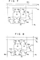
- Fig. 7 shows a circuit diagram of a semiconductor device according to another embodiment of this invention.
- This semiconductor memory circuit is the same as the semiconductor memory device shown in Fig. 1 except that it has a write control line WCL arranged for each row and an NPN transistor TR9 having its first and second collectors connected to the bases of transistors TR1 and TR2, respectively, its emitter connected to the emitter of the transistor TR2 and its base connected to the write control line.
- a write operation is carried out, a desired first row select line is set at a low level potential and with another first low select line held at a high level potential the write control line WCL for each row is set temporarily at a high level.
- the transistor TR9 is rendered conductive and the bases of the transistors TR1 and TR2 are set at a ground potential.
- the semiconductor memory circuit shown in Fig. 7 has the same effect as that of the semiconductor memory circuit shown in Fig. 5. Note that in the circuit'shown in Fig. 7 the first collector of the transistor TR9 may be omitted.
- Figs. 8 and 9 show a circuit arrangement of a semiconductor memory according to another embodiment of this invention.
- This semiconductor memory circuit is substantially similar to the semiconductor memory circuit shown in Fig. 1 except that it has a pair of data lines DL, IDL supplied with data having a mutually inverting relation and a PNP transistor TRIO having its emitter connected to the data line IDL, its base connected to the emitter of a transistor TR2 and its collector connected to the base of a transistor TR1.
- the emitter, base and collector of the transistor TRIO are formed of a P-type region 32, N-type substrate 8 (Fig. 2) and P-type region 16, respectively.
- a writing operation is effected, a desired row select line is set at a low potential level and with another first row select line held at a high potential level data "0" and .”1" are supplied to the data lines DL and IDL and the transistors TR1 and TR2 are rendered selectively conductive according to the data.
- the transistors TR1 and TR2 be constructed such that the transistors TR1 and TR2 have a different base area as in the embodiment shown in Figs. 1 to 4.
- the transistor TR2 in order that the time required for the transistor TR2 to be rendered conductive may be made longer than the time required for the transistor TR1 to be rendered conductive, the transistor TR2 is constructed such that it has a base area greater than that of the transistor TR1. Even if the other dimension, for example the collector area, of the transistors TR1 and TR2 is varied, the same result can be obtained.
- transistors TR1 and TR2 constructed in substantially the same way and the inherent electrostatic capacities of the transistors TR1 and TR2 made equal to each other, the same result is obtained even if the impedance value of the transistor TR3 is made greater than the impedance value of the transistor TR4.
- a second collector may be formed on the transistor TR1 and the base of the transistor TR6 and collector of the transistor TR7 be connected to the second collector of the transistor TR1.
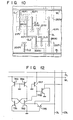
- the collector of the transistor TR6 is connected to the data line DL, as shown in Figs. 11 and 12 for example, an output data line ODL may be arranged separately from the data line DL and the collector of the transistor TR6 or TR8 may be connected to the output data line ODL.
Landscapes
- Engineering & Computer Science (AREA)
- Microelectronics & Electronic Packaging (AREA)
- Computer Hardware Design (AREA)
- Static Random-Access Memory (AREA)
- Semiconductor Memories (AREA)
Applications Claiming Priority (8)
| Application Number | Priority Date | Filing Date | Title |
|---|---|---|---|
| JP121189/78 | 1978-10-03 | ||
| JP53121190A JPS5942986B2 (ja) | 1978-10-03 | 1978-10-03 | 半導体メモリセル |
| JP121190/78 | 1978-10-03 | ||
| JP53121189A JPS5950229B2 (ja) | 1978-10-03 | 1978-10-03 | 半導体メモリセル |
| JP12860178A JPS5555496A (en) | 1978-10-20 | 1978-10-20 | Semiconductor memory cell |
| JP128602/78 | 1978-10-20 | ||
| JP12860278A JPS5555497A (en) | 1978-10-20 | 1978-10-20 | Semiconductor memory device |
| JP128601/78 | 1978-10-20 |
Publications (3)
| Publication Number | Publication Date |
|---|---|
| EP0020769A1 true EP0020769A1 (de) | 1981-01-07 |
| EP0020769A4 EP0020769A4 (de) | 1981-10-27 |
| EP0020769B1 EP0020769B1 (de) | 1984-07-11 |
Family
ID=27470758
Family Applications (1)
| Application Number | Title | Priority Date | Filing Date |
|---|---|---|---|
| EP79901095A Expired EP0020769B1 (de) | 1978-10-03 | 1980-04-22 | Speichervorrichtung mit halbleiter |
Country Status (4)
| Country | Link |
|---|---|
| US (1) | US4366554A (de) |
| EP (1) | EP0020769B1 (de) |
| DE (1) | DE2967103D1 (de) |
| WO (1) | WO1980000761A1 (de) |
Cited By (2)
| Publication number | Priority date | Publication date | Assignee | Title |
|---|---|---|---|---|
| EP0166043A1 (de) * | 1984-06-25 | 1986-01-02 | International Business Machines Corporation | MTL-Speicherzelle mit inhärenter Mehrfachfähigkeit |
| EP0233968A1 (de) * | 1986-02-21 | 1987-09-02 | Ibm Deutschland Gmbh | Statische Speicherzelle ohne Taktgeber |
Families Citing this family (5)
| Publication number | Priority date | Publication date | Assignee | Title |
|---|---|---|---|---|
| JPS57167675A (en) * | 1981-04-08 | 1982-10-15 | Nec Corp | Semiconductor device |
| US4813017A (en) * | 1985-10-28 | 1989-03-14 | International Business Machines Corportion | Semiconductor memory device and array |
| JPH0722762Y2 (ja) * | 1989-07-31 | 1995-05-24 | 日本電気株式会社 | 磁気ディスク用スピンドル・ロック装置 |
| US5276638A (en) * | 1991-07-31 | 1994-01-04 | International Business Machines Corporation | Bipolar memory cell with isolated PNP load |
| JPH0660644A (ja) * | 1992-08-05 | 1994-03-04 | Takayama:Kk | メモリーデバイス |
Family Cites Families (6)
| Publication number | Priority date | Publication date | Assignee | Title |
|---|---|---|---|---|
| NL7408502A (nl) * | 1973-07-06 | 1975-12-30 | Philips Nv | Geheugenmatrix. |
| JPS5837699B2 (ja) * | 1974-12-16 | 1983-08-18 | 三菱電機株式会社 | ハンドウタイキオクソウチ |
| US3986178A (en) * | 1975-07-28 | 1976-10-12 | Texas Instruments | Integrated injection logic random access memory |
| JPS5246735A (en) * | 1975-10-11 | 1977-04-13 | Hitachi Ltd | Semiconductor storage device |
| JPS53121589A (en) * | 1977-03-31 | 1978-10-24 | Toshiba Corp | Semiconductor logic circuit device |
| DE2964943D1 (en) * | 1978-05-11 | 1983-04-07 | Nippon Telegraph & Telephone | Semiconductor integrated memory circuit |
-
1979
- 1979-09-04 US US06/198,953 patent/US4366554A/en not_active Expired - Lifetime
- 1979-09-04 WO PCT/JP1979/000235 patent/WO1980000761A1/ja not_active Ceased
- 1979-09-04 DE DE7979901095T patent/DE2967103D1/de not_active Expired
-
1980
- 1980-04-22 EP EP79901095A patent/EP0020769B1/de not_active Expired
Cited By (2)
| Publication number | Priority date | Publication date | Assignee | Title |
|---|---|---|---|---|
| EP0166043A1 (de) * | 1984-06-25 | 1986-01-02 | International Business Machines Corporation | MTL-Speicherzelle mit inhärenter Mehrfachfähigkeit |
| EP0233968A1 (de) * | 1986-02-21 | 1987-09-02 | Ibm Deutschland Gmbh | Statische Speicherzelle ohne Taktgeber |
Also Published As
| Publication number | Publication date |
|---|---|
| US4366554A (en) | 1982-12-28 |
| DE2967103D1 (en) | 1984-08-16 |
| EP0020769B1 (de) | 1984-07-11 |
| EP0020769A4 (de) | 1981-10-27 |
| WO1980000761A1 (fr) | 1980-04-17 |
Similar Documents
| Publication | Publication Date | Title |
|---|---|---|
| US3390382A (en) | Associative memory elements employing field effect transistors | |
| KR100207941B1 (ko) | 공유 BiCMOS 감지 증폭기 | |
| US4078261A (en) | Sense/write circuits for bipolar random access memory | |
| EP0023792B1 (de) | Halbleiterspeicher mit integrierten injektionslogischen Speicherzellen | |
| US3969708A (en) | Static four device memory cell | |
| US4682200A (en) | Semiconductor memory device with matched equivalent series resistances to the complementary data lines | |
| KR19980063319A (ko) | 스테이틱형 반도체 기억 장치 | |
| US4366554A (en) | I2 L Memory device | |
| JPH0316717B2 (de) | ||
| KR900004327B1 (ko) | 센스증폭기와 프로그래밍회로 각각에 독립으로 칼럼 트랜지스터 게이트 트랜스터 그룹을 갖게한 반도체 기억장치 | |
| US4651302A (en) | Read only memory including an isolation network connected between the array of memory cells and the output sense amplifier whereby reading speed is enhanced | |
| EP0028157B1 (de) | Integrierte Halbleiterspeicherschaltung mit integrierter Injektionslogik | |
| EP0222154B1 (de) | Halbleiterspeichervorrichtung und -matrixanordnung | |
| US4292675A (en) | Five device merged transistor RAM cell | |
| JPH04285794A (ja) | 半導体記憶装置 | |
| US3820086A (en) | Read only memory(rom)superimposed on read/write memory(ram) | |
| US4910711A (en) | Bicmos read/write control and sensing circuit | |
| EP0418794B1 (de) | Halbleiterspeicheranordnung | |
| EP0058845B1 (de) | Speicherzelle für RAM | |
| EP0023408B1 (de) | Halbleiterspeicher mit integrierten injektionslogischen Speicherzellen | |
| US3821719A (en) | Semiconductor memory | |
| US4313179A (en) | Integrated semiconductor memory and method of operating same | |
| US4439842A (en) | Bipolar transistor read only or read-write store with low impedance sense amplifier | |
| EP0685850B1 (de) | Integrierte Halbleiterschaltung mit einer SRAM-Zellenmatrix mit einseitiger Stromabfühlschaltung | |
| US4589096A (en) | IIL semiconductor memory including arrangement for preventing information loss during read-out |
Legal Events
| Date | Code | Title | Description |
|---|---|---|---|
| PUAI | Public reference made under article 153(3) epc to a published international application that has entered the european phase |
Free format text: ORIGINAL CODE: 0009012 |
|
| 17P | Request for examination filed |
Effective date: 19800602 |
|
| AK | Designated contracting states |
Designated state(s): DE FR GB |
|
| GRAA | (expected) grant |
Free format text: ORIGINAL CODE: 0009210 |
|
| AK | Designated contracting states |
Designated state(s): DE FR GB |
|
| REF | Corresponds to: |
Ref document number: 2967103 Country of ref document: DE Date of ref document: 19840816 |
|
| RAP2 | Party data changed (patent owner data changed or rights of a patent transferred) |
Owner name: KABUSHIKI KAISHA TOSHIBA |
|
| ET | Fr: translation filed | ||
| REG | Reference to a national code |
Ref country code: FR Ref legal event code: CD |
|
| PLBE | No opposition filed within time limit |
Free format text: ORIGINAL CODE: 0009261 |
|
| STAA | Information on the status of an ep patent application or granted ep patent |
Free format text: STATUS: NO OPPOSITION FILED WITHIN TIME LIMIT |
|
| 26N | No opposition filed | ||
| REG | Reference to a national code |
Ref country code: GB Ref legal event code: 746 |
|
| PGFP | Annual fee paid to national office [announced via postgrant information from national office to epo] |
Ref country code: GB Payment date: 19950824 Year of fee payment: 17 |
|
| PGFP | Annual fee paid to national office [announced via postgrant information from national office to epo] |
Ref country code: FR Payment date: 19950911 Year of fee payment: 17 |
|
| PGFP | Annual fee paid to national office [announced via postgrant information from national office to epo] |
Ref country code: DE Payment date: 19950918 Year of fee payment: 17 |
|
| PG25 | Lapsed in a contracting state [announced via postgrant information from national office to epo] |
Ref country code: GB Effective date: 19960904 |
|
| PG25 | Lapsed in a contracting state [announced via postgrant information from national office to epo] |
Ref country code: FR Effective date: 19960930 |
|
| GBPC | Gb: european patent ceased through non-payment of renewal fee |
Effective date: 19960904 |
|
| PG25 | Lapsed in a contracting state [announced via postgrant information from national office to epo] |
Ref country code: DE Effective date: 19970603 |
|
| REG | Reference to a national code |
Ref country code: FR Ref legal event code: ST |
|
| REG | Reference to a national code |
Ref country code: FR Ref legal event code: ST |