EP0042175A2 - Procédé de fabrication d'un dispositif semiconducteur à structure SOS - Google Patents
Procédé de fabrication d'un dispositif semiconducteur à structure SOS Download PDFInfo
- Publication number
- EP0042175A2 EP0042175A2 EP81104653A EP81104653A EP0042175A2 EP 0042175 A2 EP0042175 A2 EP 0042175A2 EP 81104653 A EP81104653 A EP 81104653A EP 81104653 A EP81104653 A EP 81104653A EP 0042175 A2 EP0042175 A2 EP 0042175A2
- Authority
- EP
- European Patent Office
- Prior art keywords
- layer
- semiconductor
- single crystalline
- grown
- main surface
- Prior art date
- Legal status (The legal status is an assumption and is not a legal conclusion. Google has not performed a legal analysis and makes no representation as to the accuracy of the status listed.)
- Granted
Links
Images
Classifications
-
- H—ELECTRICITY
- H10—SEMICONDUCTOR DEVICES; ELECTRIC SOLID-STATE DEVICES NOT OTHERWISE PROVIDED FOR
- H10D—INORGANIC ELECTRIC SEMICONDUCTOR DEVICES
- H10D86/00—Integrated devices formed in or on insulating or conducting substrates, e.g. formed in silicon-on-insulator [SOI] substrates or on stainless steel or glass substrates
-
- H—ELECTRICITY
- H10—SEMICONDUCTOR DEVICES; ELECTRIC SOLID-STATE DEVICES NOT OTHERWISE PROVIDED FOR
- H10D—INORGANIC ELECTRIC SEMICONDUCTOR DEVICES
- H10D30/00—Field-effect transistors [FET]
- H10D30/60—Insulated-gate field-effect transistors [IGFET]
- H10D30/67—Thin-film transistors [TFT]
- H10D30/6758—Thin-film transistors [TFT] characterised by the insulating substrates
- H10D30/6759—Silicon-on-sapphire [SOS] substrates
-
- H—ELECTRICITY
- H10—SEMICONDUCTOR DEVICES; ELECTRIC SOLID-STATE DEVICES NOT OTHERWISE PROVIDED FOR
- H10P—GENERIC PROCESSES OR APPARATUS FOR THE MANUFACTURE OR TREATMENT OF DEVICES COVERED BY CLASS H10
- H10P14/00—Formation of materials, e.g. in the shape of layers or pillars
- H10P14/20—Formation of materials, e.g. in the shape of layers or pillars of semiconductor materials
- H10P14/24—Formation of materials, e.g. in the shape of layers or pillars of semiconductor materials using chemical vapour deposition [CVD]
-
- H—ELECTRICITY
- H10—SEMICONDUCTOR DEVICES; ELECTRIC SOLID-STATE DEVICES NOT OTHERWISE PROVIDED FOR
- H10P—GENERIC PROCESSES OR APPARATUS FOR THE MANUFACTURE OR TREATMENT OF DEVICES COVERED BY CLASS H10
- H10P14/00—Formation of materials, e.g. in the shape of layers or pillars
- H10P14/20—Formation of materials, e.g. in the shape of layers or pillars of semiconductor materials
- H10P14/29—Formation of materials, e.g. in the shape of layers or pillars of semiconductor materials characterised by the substrates
- H10P14/2901—Materials
- H10P14/2921—Materials being crystalline insulating materials
-
- H—ELECTRICITY
- H10—SEMICONDUCTOR DEVICES; ELECTRIC SOLID-STATE DEVICES NOT OTHERWISE PROVIDED FOR
- H10P—GENERIC PROCESSES OR APPARATUS FOR THE MANUFACTURE OR TREATMENT OF DEVICES COVERED BY CLASS H10
- H10P14/00—Formation of materials, e.g. in the shape of layers or pillars
- H10P14/20—Formation of materials, e.g. in the shape of layers or pillars of semiconductor materials
- H10P14/29—Formation of materials, e.g. in the shape of layers or pillars of semiconductor materials characterised by the substrates
- H10P14/2926—Crystal orientations
-
- H—ELECTRICITY
- H10—SEMICONDUCTOR DEVICES; ELECTRIC SOLID-STATE DEVICES NOT OTHERWISE PROVIDED FOR
- H10P—GENERIC PROCESSES OR APPARATUS FOR THE MANUFACTURE OR TREATMENT OF DEVICES COVERED BY CLASS H10
- H10P14/00—Formation of materials, e.g. in the shape of layers or pillars
- H10P14/20—Formation of materials, e.g. in the shape of layers or pillars of semiconductor materials
- H10P14/32—Formation of materials, e.g. in the shape of layers or pillars of semiconductor materials characterised by intermediate layers between substrates and deposited layers
- H10P14/3202—Materials thereof
- H10P14/3204—Materials thereof being Group IVA semiconducting materials
- H10P14/3211—Silicon, silicon germanium or germanium
-
- H—ELECTRICITY
- H10—SEMICONDUCTOR DEVICES; ELECTRIC SOLID-STATE DEVICES NOT OTHERWISE PROVIDED FOR
- H10P—GENERIC PROCESSES OR APPARATUS FOR THE MANUFACTURE OR TREATMENT OF DEVICES COVERED BY CLASS H10
- H10P14/00—Formation of materials, e.g. in the shape of layers or pillars
- H10P14/20—Formation of materials, e.g. in the shape of layers or pillars of semiconductor materials
- H10P14/32—Formation of materials, e.g. in the shape of layers or pillars of semiconductor materials characterised by intermediate layers between substrates and deposited layers
- H10P14/3258—Crystal orientation
-
- H—ELECTRICITY
- H10—SEMICONDUCTOR DEVICES; ELECTRIC SOLID-STATE DEVICES NOT OTHERWISE PROVIDED FOR
- H10P—GENERIC PROCESSES OR APPARATUS FOR THE MANUFACTURE OR TREATMENT OF DEVICES COVERED BY CLASS H10
- H10P14/00—Formation of materials, e.g. in the shape of layers or pillars
- H10P14/20—Formation of materials, e.g. in the shape of layers or pillars of semiconductor materials
- H10P14/34—Deposited materials, e.g. layers
- H10P14/3402—Deposited materials, e.g. layers characterised by the chemical composition
- H10P14/3404—Deposited materials, e.g. layers characterised by the chemical composition being Group IVA materials
- H10P14/3411—Silicon, silicon germanium or germanium
-
- H—ELECTRICITY
- H10—SEMICONDUCTOR DEVICES; ELECTRIC SOLID-STATE DEVICES NOT OTHERWISE PROVIDED FOR
- H10P—GENERIC PROCESSES OR APPARATUS FOR THE MANUFACTURE OR TREATMENT OF DEVICES COVERED BY CLASS H10
- H10P14/00—Formation of materials, e.g. in the shape of layers or pillars
- H10P14/20—Formation of materials, e.g. in the shape of layers or pillars of semiconductor materials
- H10P14/34—Deposited materials, e.g. layers
- H10P14/3438—Doping during depositing
- H10P14/3441—Conductivity type
- H10P14/3442—N-type
-
- H—ELECTRICITY
- H10—SEMICONDUCTOR DEVICES; ELECTRIC SOLID-STATE DEVICES NOT OTHERWISE PROVIDED FOR
- H10P—GENERIC PROCESSES OR APPARATUS FOR THE MANUFACTURE OR TREATMENT OF DEVICES COVERED BY CLASS H10
- H10P14/00—Formation of materials, e.g. in the shape of layers or pillars
- H10P14/20—Formation of materials, e.g. in the shape of layers or pillars of semiconductor materials
- H10P14/38—Formation of materials, e.g. in the shape of layers or pillars of semiconductor materials characterised by treatments done after the formation of the materials
- H10P14/3802—Crystallisation or recrystallisation of non-monocrystalline semiconductor materials, e.g. regrowth
- H10P14/3808—Crystallisation or recrystallisation of non-monocrystalline semiconductor materials, e.g. regrowth using laser beams
- H10P14/3816—Pulsed laser beam
-
- H—ELECTRICITY
- H10—SEMICONDUCTOR DEVICES; ELECTRIC SOLID-STATE DEVICES NOT OTHERWISE PROVIDED FOR
- H10P—GENERIC PROCESSES OR APPARATUS FOR THE MANUFACTURE OR TREATMENT OF DEVICES COVERED BY CLASS H10
- H10P34/00—Irradiation with electromagnetic or particle radiation of wafers, substrates or parts of devices
- H10P34/40—Irradiation with electromagnetic or particle radiation of wafers, substrates or parts of devices with high-energy radiation
- H10P34/42—Irradiation with electromagnetic or particle radiation of wafers, substrates or parts of devices with high-energy radiation with electromagnetic radiation, e.g. laser annealing
-
- Y—GENERAL TAGGING OF NEW TECHNOLOGICAL DEVELOPMENTS; GENERAL TAGGING OF CROSS-SECTIONAL TECHNOLOGIES SPANNING OVER SEVERAL SECTIONS OF THE IPC; TECHNICAL SUBJECTS COVERED BY FORMER USPC CROSS-REFERENCE ART COLLECTIONS [XRACs] AND DIGESTS
- Y10—TECHNICAL SUBJECTS COVERED BY FORMER USPC
- Y10S—TECHNICAL SUBJECTS COVERED BY FORMER USPC CROSS-REFERENCE ART COLLECTIONS [XRACs] AND DIGESTS
- Y10S117/00—Single-crystal, oriented-crystal, and epitaxy growth processes; non-coating apparatus therefor
- Y10S117/903—Dendrite or web or cage technique
- Y10S117/904—Laser beam
-
- Y—GENERAL TAGGING OF NEW TECHNOLOGICAL DEVELOPMENTS; GENERAL TAGGING OF CROSS-SECTIONAL TECHNOLOGIES SPANNING OVER SEVERAL SECTIONS OF THE IPC; TECHNICAL SUBJECTS COVERED BY FORMER USPC CROSS-REFERENCE ART COLLECTIONS [XRACs] AND DIGESTS
- Y10—TECHNICAL SUBJECTS COVERED BY FORMER USPC
- Y10S—TECHNICAL SUBJECTS COVERED BY FORMER USPC CROSS-REFERENCE ART COLLECTIONS [XRACs] AND DIGESTS
- Y10S438/00—Semiconductor device manufacturing: process
- Y10S438/967—Semiconductor on specified insulator
Definitions
- This invention relates to a semiconductor device having an insulating substrate which has at least one main surface, and a semiconductor layer which is deposited on the main surface of the insulating substrate, as well as a method for making the same.
- a semiconductor substrate for forming a semiconductor integrated circuit device there has been proposed a structure in which a semiconductor single crystalline layer of Si or the like is grown on a high insulating single crystalline substrate of sapphire, spinel or the like.
- the semiconductor single crystalline layer in which semiconductor elements are to be formed can be made quite thin without spoiling the mechanical strength, while at the same time a high insulation is achieved between the layer and the substrate, so that an IC can be realized having a high operating speed, a high integration and a low power dissipation.
- the SOS structure can be fabricated by a method similar to the epitaxial growth of a semiconductor having hitherto been known well.
- a satisfactory crystalline quality is difficult to be obtained for the reasons that an insulator which is widely different from a semiconductor in points of the lattice constant and the coefficient of thermal expansion is employed for the substrate and that the required thickness of the semiconductor single crystalline layer is extremely small, that is at most about 1 ⁇ m.
- the mobility of carriers within the semiconductor single crystalline layer has to be relatively high.
- prior art SOS structures however, it has been difficult to make the mobility of carriers at least as high as in bulk semiconductor elements. Therefore, up to now the usage of SOS structures for high-speed ICs has been rather limited.
- the mobility of carriers within semiconductor elements is lowered by all factors which can scatter the carriers.
- factors are, for example, the lattice of the semiconductor crystal, the impurity atoms with which the semiconductor is doped, stacking faults, dislocations and mechanical strains.
- the stacking faults, discloations and mechanical strains are included in large quantities in the SOS structure and have rendered it difficult to raise the mobility.
- the substrate and the semiconductor to be grown thereon differ in the lattic constant, and both define the so-called heterojunction, so that twins, dislocations or stacking faults appear in large numbers at the interface of the two layers.
- the number of such disorders decreases gradually with the growth of the semiconductor. Since, however, the semiconductor layer is very thin - for example, 0.5 - 1 um in case of an IC of the SOS structure - it cannot be avoided to use as active parts.-of a semiconductor element regions in which the disorders have not decreased sufficiently. It has therefore been impossible to obtain a sufficiently high mobility. Due to the same cause, it has been impossible to make the leakage current of the semiconductor element low enough.
- this object can be obtained by a semiconductor layer consisting of an interface layer which adjoins said main surface of said insulating substrate and which is made up of a large number of single crystalline grains, a seed crystalline layer which adjoins said interface layer and which is made up of a substantially uniform single crystalline layer, and a re-grown layer which adjoins said seed crystalline layer and extends to the top main surface of said semiconductor layer and which has a thickness greater than that of said seed crystalline layer, whereby the seed crystalline layer determines the crystalline quality of said re-grown layer and whereby the regrown layer is being formed through irradiation with an electromagnetic wave, thereby obtaining a lattice structure different from that of the deposited layer.
- the semiconductor layer comprises an interface layer made of twins which adjoins a substrate and which is an aggregate of a large number of semiconductor single crystalline grains, a seed layer which adjoins the interface layer and which has a fixed orientation, and a re-grown single crystalline layer which adjoins the seed layer and reaches a top surface of the semiconductor layer and which is much thicker than the twin layer and the seed layer.
- the re- grown layer is being formed in such a way that its original or starting deposited layer is irradiated with an electromagnetic wave under adequate irradiation conditions, thereby to be regrown with the crystal of the seed layer as a seed into a crystalline quality different from that of the deposited layer.
- the parameters of the irradiation with electromagnetic waves for the re-growth are selected in such'a way that the electromagnetic waves act substantially on almost all the region of the deposited single crystalline semiconductor layer (except the portion to serve as the seed layer) and may re-grow the portion under the action.
- the "re-growth” is, in the broadest sense, the process of the rearrangement of atoms and is typified by the melting - solidification process.
- the inventors' study has revealed that, in order to enhance the operating speed and reduce the leakage current of a semiconductor device, for example, a MOS transistor fabricated with the SOS structure, an improvement of only the crystalline quality of the top surface of the semiconductor layer is insufficient, so that the crystalline quality of the bulk semiconductor layer has to be changed. According to this invention, such requirement or necessity is fully met.
- the seed layer in this invention is necessary for rendering the re-grown layer single crystalline.
- the irradiation with the electromagnetic wave has to be such that the seed layer per se is not re-grown, because the twin layer acts as seed for the re-growth layer, so that the re-grown layer would become polycrystalline or amorphous, which in case of this invention has to be avoided.
- the semiconductor is Si
- the SOS structure is not subjected to a heat treatment by which the substrate and the Si layer are simultaneously heated to 600 0 C or above, it is favorable that the top main surface of the single crystalline Si 'layer has a crystal orientation of ⁇ 100 ⁇ or ⁇ 110 ⁇ .
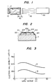
- a method.for making an SOS structure according to this invention will be exemplified with reference to Figure 1.
- a single crystalline sapphire substrate 1 having a diameter of approximately 50 mm, a thickness of approximately 0.3 mm and an orientation of (1102) wa.s prepared.
- a Si layer 2 with an orientation of (100) was epitaxially grown on the sapphire substrate by pyrolyzing silane (SiH 4 ) in a hydrogen atmosphere at 1,020 °C.
- Phosphine was used as a dopant source to achieve a donor level of about 3 x 10 16 cm 3 .
- the electron Hall mobility in the Si layer 2 of this SOS structure was about 240 cm 2 /V ⁇ s on the average.
- the crystal faces of Si grown first are the two sorts of (100) and (110).
- the Si does not become single crystalline but becomes a polycrystalline region in which two sorts of crystal grains of the different crystal faces aggregate. In the present invention, this region shall be termed the "interface layer".
- Such interface layer is formed up to a thickness of approximately 0.05 ⁇ m from the sapphire substrate by the conventional vapor growth, and contains in large quantities stacking faults, Al atoms and 0 atoms introduced from the sapphire substrate by the auto-doping, Si atoms not contributing to the formation of the crystal, and so forth.
- the Si layer over the interface layer becomes a single crystalline layer whose crystal face is (100). In the grown state left intact, however, it still includes large numbers of stacking faults and dislocations, so that the mobility of carriers remains at the low value as described above.
- the SOS structure was irradiated with a laser beam as shown in Figure 1.
- numeral 10 designates the SOS structure consisting of the sapphire substrate 1 and the n-type single crystalline Si layer 2.
- Numeral 20 indicates a laser source, numeral 30 the laser beam emitted from the laser source 20, and numeral 40 a device for making the laser beam 30 uniform.
- the device 40 consists of a scatterer 41 and a reflector 42.
- the laser source 20 used in this example was a Q-switched ruby laser, the wavelength a-of which was 694.3 nm and the pulse width of one irradiation of which was 25 nsec.
- As the scatterer 41 a plate of ground glass is usable.
- the reflector 42 Usable as the reflector 42 is a quartz cylinder whose inner surface is coated with a reflective material.
- the energy of the laser was made the three magnitudes of 1.0 J/cm 2 , 1.5 J/cm 2 and 2.5 J/cm 2 , and the Hall mobility of the Si layer 2 after the irradiation was measured as to the respective cases.
- the mobility is in a substantially proportional relationship with the operating speed of an element.
- the Hall mobility after the irradiation did not exhibit a substantial change from that before the irradiation.
- the irradiation was conducted repeatedly in a range of two times to five times, the Hall mobility did not substantially change from the value of the Si layer without the irradiation yet.
- the Hall mobility after the first irradiation was 270 cm2 / V ⁇ s on the average and merely increased to some extent in comparison with the value before the irradiation.
- the Hall mobility exhibited large values in all the operations in such manner that the value after the second irradiation was approximately 540 cm 2 /V ⁇ s and increased above double in comparison with the value of the Si layer without the irradiation, that the value after the third, irradiation was approximately 560 cm 2 /V ⁇ s, and that the value after the fourth irradiation was approximately 580 cm 2 /V ⁇ s.
- the Hall mobility became as extremely low as approximately 10 cm 2 /V ⁇ s.
- the n-type Si layer was inverted into the p-type.
- the Si layers of the SOS structures subjected to the two or more times of irradiation and re-growth steps at the energy density of 1.5 J/cm 2 had disorders etched selectively, and the resultant surfaces were observed with a scanning electron microscope. As a result, the stacking faults were hardly observed, and the number of etch pits corresponding to the dislocations decreased to 1/3 - 1/5 in comparison with the number in the Si layer not irradiated.
- the cause by which the Hall mobility was lowered in the extreme at the energy density of 2.5 J/cm 2 is conjectured to be that since the energy was excessive for the Si layer used in the example, the entire Si layer including the interface layer was molten by the irradiation, with the result that the crystal to serve as the seed during the re-growth turned into twins and that a polycrystalline or amorphous Si layer was re-grown.
- the cause for the p-type inversion is conjectured to be that since the interface between the sapphire substrate and the Si layer was excessively heated, the Al atoms in the sapphire substrate were introduced into the molten Si and spread into the Si layer along with the re-growth of Si.
- the thickness of the Si layer of the SOS structure for use in an IC is ordinarily 0.4 - 0.5 ⁇ m or greater, the effect of this invention cannot be expected with the low-energy laser of such short wavelength.
- a short-wavelength laser is operated at high energy, unfavorably the surface of the Si layer is overheated near to the boiling point of Si to worsen the crystalline quality in the surface because most of the energy is absorbed by the surface part.
- a MOS type transistor such worsening of the crystalline quality in the Si surface appears as the dispersion of the threshold voltage V th . In this manner, the electromagnetic wave for use in the present invention needs to melt or re-grow substantially the whole semiconductor layer uniformly.
- the Hall mobility after repeating the irradiation five or more times was approximately 380 cm2/V.s lower than the value after repeating the irradiation two to four times. Accordingly, the repeated irradiation of 2 - 4 times is desirable under the irradiation conditions stated above.
- FIG. 2 As the SOS structure, one prepared by the foregoing process was used.. In the melting and re-growing process by the irradiation with the laser beam, the energy density was 1.5 J/cm 2 and the number of times of the irradiation was three. Using known photolithography, selective diffusion, oxide-film forming technique etc., a MOS transistor shown in Figure 2 was formed in the Si layer of this SOS structure.
- numeral 212 designates a source region, numeral 211 a drain region, numerals 205, 204 and 206 source, drain and gate electrodes respectively, and numeral 201 an Si0 2 film.
- the source-drain leakage current was approximately 6 x 10 -13 A/fm.
- the source-drain leakage current of a MOS transistor fabricated by the use of an SOS structure which was formed similarly to the above example except that the laser irradiation according to this invention was not performed was approximately 3 x 10 -11 A/ ⁇ m and was inferior to the value of the above example.
- the leakage current can be made much lower, and hence, the industrial production of a dynamic MOS ⁇ LSI etc. having hitherto been difficult of fabrication with the SOS structure is permitted.
- the orientation of the top main surface of the Si layer of the SOS structure is made ⁇ 111 ⁇ .
- This embodiment is the same as the foregoing embodiment in point of employing the melting and re-growing process by the laser beam.
- the reason why the orientation of ⁇ 111 ⁇ is selected in this embodiment is as follows.
- a substrate is greater than a semiconductor in the coefficient of thermal expansion.
- a compressive stress remains in the semiconductor on account of the difference between the coefficients of thermal expansion. Due to the compressive stress, the mobility in the SOS structure lowers.
- the crystal face ⁇ 111 ⁇ which is the general term of the crystal face (111) and faces crystallographically equivalent thereto is free from the degradation of the mobility upon the application of the compressive stress in contrast to the other crystal faces.
- the present embodiment utilizes both the favorable property .of the ⁇ 111 ⁇ face of Si and disorder reducing processings including the melting treatment with the laser beam.
- the SOS structure was irradiated with the beam of the Q-switched ruby laser to carry out the process for melting and re-growing the Si layer.
- the energy density was made 1.5 J/cm 2 and the irradiation was conducted three times, whereby a MOS transistor as shown in Figure 2 was fabricated.
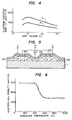
- gate voltage gate - source voltage
- electron Hall mobility the mobility of a channel region (the surface part of the p-type Si region opposing to the gate electrode), and is also called the "channel mobility”.
- the present embodiment A has sharply increased in both the Hall mobility and the channel mobility relative to the comparative example B.
- the operating speed is proportional to the channel mobility. It is accordingly understood from Figure 4 that, in comparison with the comparative example, the present embodiment has sharply increased in the operating speed of the MOS transistor.
- the present embodiment is applicable to all kinds of semiconductor devices having SOS structures, but it is particularly suitable for a semiconductor device both in which/a PMOS type semiconductor element and an NMOS type semiconductor element exist in an identical SOS structure, for example, a semiconductor device which includes CMOS transistors.
- CMOS transistors for example, a semiconductor device which includes CMOS transistors.
- the Si single crystal having the crystal face ⁇ 111 ⁇ used in the present embodiment exhibits higher mobilities in both the p-type and the n-type under the action of the compressive stress than in the unstressed condition.
- the Si single crystal having the crystal face ⁇ 111 ⁇ has its effective mobility in the n-type Si raised to approximately 103 % and its effective mobility in the p-type Si raised to approximately 130 % with respect to the values in the unstressed condition. Accordingly, the operating speeds of the CMOS transistors increase.
- Figure 5 shows an example of such CMOS transistors. Symbols used are the same as in Figure 2. In Figure 5, a transistor on the left side is of the PMOS type, and a transistor on the right side is of the NMOS type. Figure 5 also illustrates an example of interconnections in the case of employing these transistors as an inverter.
- the present embodiment is characterized, in a semiconductor device of the SOS structure, in that the facial orientation of a Si single crystalline layer is made ⁇ 100 ⁇ or ⁇ 110 ⁇ and that the portion of the Si single crystalline layer including at least the exposed main surface thereof is put into a re-grown layer on which a tensile stress acts.
- the tensile stress is applied to the Si layer whose facial orientation is ⁇ 100 ⁇ or ⁇ 110 ⁇ , the mobility of the Si layer increases.
- the inventors' experiment has revealed, however, that the mobility degrades when the SOS structure with its mobility thus increased is subjected to a high-temperature heat treatment for fabricating a semiconductor device, such as doping with an impurity.
- the present embodiment prevents the degradation of the mobility by a method to be described below.
- FIG. 6 This figure illustrates the electron Hall mobilities within the Si single crystalline layer at the times when the SOS structure having the Si layer of the (100) crystal the mobility of which has been enhanced owing to the laser irradiation according to this invention has been annealed at various temperatures.
- the annealing was conducted for the whole SOS structure, and the period of time thereof was about 40 minutes at any of the temperatures.
- the annealing temperature is below 600 °C
- the effect of the increase of the mobility appears more or less with respect to the SOS structure not irradiated by the laser, but it cannot be expected at or above 600 °C.
- An annealing temperature of or below 400 °C is favorable because the mobility increased by the laser irradiation is not degraded.
- the semiconductor device is produced by forming the re-grown layer according to this invention and thereafter holding at least one of the substrate and the Si single crystalline layer at a temperature below 600 °C, desirably of or below 400 °C.
- the present embodiment is applicable to the above-stated Si single crystalline layer having the facial orientation of (100), and besides, to Si single crystalline layers whose main surfaces are faces generally equivalent to the face (100) in the crystallographic sense (the faces are denoted by the ⁇ 100 ⁇ face) and the ⁇ 110 ⁇ face.
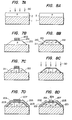
- Figures 7A to 7D F ference will be had to Figures 7A to 7D.
- a p-type Si single crystalline layer 2 whose main surface has the facial orientation of (100) was vapor-grown at about 1,000 °C.
- the single crystalline layer 2 was irradiated with beam 30 to form a re-grown layer.
- the conditions of the irradiation were the same as stated before.
- the Si single crystalline layer 2 was selectively etched with a KOH solution at the normal temperature, thereby to form a Si single crystalline island 210.
- a Si0 2 film 201 and a Si polycrystalline layer 202 were successively deposited by the plasma CVD process at about 400 °C, whereupon their parts other than parts to serve as the gate portion of the MOS transistor were removed by the photolithography.
- the highest temperature in the application of the photolithography was at the baking of a photoresist film, and the substrate temperature at this time was about 100 °C.
- those parts of the Si single crystalline island 210 which were not covered with the Si0 2 film 201 were doped with an impurity establishing the n-type, such as phosphorus, by the ion implantation process so as to form a source region 211 and a drain region 212.
- the temperature of the substrate 1 at the ion implantation was about 100 °C.
- the source region 211 and the drain region 212 were subjected to the laser annealing in order to activate the implanted ions.
- a continuous-wave laser was used. Although the temperature of the surfaces of the source region and drain region was raised to or above approximately 1,000 °C by the laser irradiation, the substrate 1 was held at the normal temperature. ( Figure 7C)
- the parts of the Si single crystalline island 210 except parts on which electrodes were to be formed were formed with Si0 2 films 203 and 207 by the plasma CVD process at about 400 °C. Thereafter, aluminum (Al) was evaporated at the normal temperature to form the source electrode 204 and the drain electrode 205. Then, the MOS transistor was finished up. (Figure 7D)
- the channel mobility in the MOS transistor of this example was 700 - 800 cm 2 /V ⁇ s. This value is much higher than the channel mobility of about 500 cm 2 /V ⁇ s in a MOS transistor employing the prior-art SOS structure which does not have the re-grown layer according to this invention.
- FIG. 8A An SOS structure similar to that shown in Figure 7A was prepared ( Figure 8A). Subsequently, single crystalline island 210 was formed as in Figure 7B. Thereafter, a source region 211 and a drain region 212 were formed by the use of the techniques of selective thermal diffusion etc. employed in the conventional production of semiconductor devices.
- the temperature of the thermal diffusion may be a high temperature of, for example, 1,150 °C. Shown at 201 is a Si0 2 film which was formed on the exposed surface of the single crystalline island 210 by the thermal diffusion step. ( Figure 8B)
- the Si single crystalline island 210 was irradiated with a laser beam 30 to form a re-grown layer within the Si single crystal.
- the laser irradiation was conducted with the apparatus shown in Figure 1, and the conditions.of the irradiation were as stated in the explanation of the features of this invention. Since the SiO 2 film 201 is transparent with respect to the laser beam 30, it does not form an obstacle to the formation of the re-grown layer. ( Figure 8C)
- the channel mobility in the MOS transistor of this example was 700 - 800 cm2/V.s as in the foregoing example illustrated in Figures 7A to 7D.
- the gate electrode was formed of the evaporated Al film, it may well be a polycrystalline Si film as in the foregoing example if desired.
- the gate electrode may well be formed of an evaporated metal film of Al or the like.
- processings other than those described above can be performed as desired.
- the pulsating laser beam having the width of 25 nsec was used.
- this invention is not restricted to the aforecited pulse width, but a beam of a width narrower or broader than 25 nsec is also effective.
- a too broad width, however, is unfavorable because the substrate such as of sapphire is feared to be overheated due to the conduction of heat, to introduce into the semiconductor such harmful impurities as Al atoms within the sapphire substrate.
- the material to which this invention is applied is not restricted to Si on sapphire, but it may be Si on spinel, Ge on sapphire, Ge on spinel, or a semiconductor on glass of SiO 2 or the like or on an insulating film such as silicon nitride film, and it may well be a compound semiconductor.
- the semiconductor element may well be others than the MOS transistor.
- this invention is effective to provide a semiconductor device in which the crystalline quality of the semiconductor layer of an SOS structure is improved to reduce the leakage current and to enhance the operating speed.
Landscapes
- Recrystallisation Techniques (AREA)
- Thin Film Transistor (AREA)
Applications Claiming Priority (2)
| Application Number | Priority Date | Filing Date | Title |
|---|---|---|---|
| JP8142080A JPS577924A (en) | 1980-06-18 | 1980-06-18 | Semiconductor device and manufacture thereof |
| JP81420/80 | 1980-06-18 |
Publications (3)
| Publication Number | Publication Date |
|---|---|
| EP0042175A2 true EP0042175A2 (fr) | 1981-12-23 |
| EP0042175A3 EP0042175A3 (en) | 1982-06-02 |
| EP0042175B1 EP0042175B1 (fr) | 1987-09-09 |
Family
ID=13745857
Family Applications (1)
| Application Number | Title | Priority Date | Filing Date |
|---|---|---|---|
| EP81104653A Expired EP0042175B1 (fr) | 1980-06-18 | 1981-06-16 | Procédé de fabrication d'un dispositif semiconducteur à structure SOS |
Country Status (4)
| Country | Link |
|---|---|
| US (1) | US4693758A (fr) |
| EP (1) | EP0042175B1 (fr) |
| JP (1) | JPS577924A (fr) |
| DE (1) | DE3176439D1 (fr) |
Families Citing this family (14)
| Publication number | Priority date | Publication date | Assignee | Title |
|---|---|---|---|---|
| JPH077829B2 (ja) * | 1981-02-02 | 1995-01-30 | 株式会社日立製作所 | 半導体装置およびその製法 |
| US4853076A (en) * | 1983-12-29 | 1989-08-01 | Massachusetts Institute Of Technology | Semiconductor thin films |
| US4727044A (en) * | 1984-05-18 | 1988-02-23 | Semiconductor Energy Laboratory Co., Ltd. | Method of making a thin film transistor with laser recrystallized source and drain |
| JPS61205501A (ja) * | 1985-03-07 | 1986-09-11 | Toyo Tire & Rubber Co Ltd | 大型バイアスタイヤ |
| JPS61271105A (ja) * | 1985-05-28 | 1986-12-01 | Bridgestone Corp | 重荷重用空気入りタイヤ |
| US5021119A (en) * | 1987-11-13 | 1991-06-04 | Kopin Corporation | Zone-melting recrystallization process |
| US5453153A (en) * | 1987-11-13 | 1995-09-26 | Kopin Corporation | Zone-melting recrystallization process |
| US4885052A (en) * | 1987-11-13 | 1989-12-05 | Kopin Corporation | Zone-melting recrystallization process |
| US5365875A (en) * | 1991-03-25 | 1994-11-22 | Fuji Xerox Co., Ltd. | Semiconductor element manufacturing method |
| JPH05335529A (ja) * | 1992-05-28 | 1993-12-17 | Fujitsu Ltd | 半導体装置およびその製造方法 |
| JPH06140704A (ja) * | 1992-10-26 | 1994-05-20 | Mitsubishi Electric Corp | レーザ光照射装置 |
| US6544825B1 (en) * | 1992-12-26 | 2003-04-08 | Semiconductor Energy Laboratory Co., Ltd. | Method of fabricating a MIS transistor |
| US6011291A (en) * | 1997-02-21 | 2000-01-04 | The United States Of America As Represented By The Secretary Of The Navy | Video display with integrated control circuitry formed on a dielectric substrate |
| KR20160108697A (ko) * | 2015-03-05 | 2016-09-20 | 현대자동차주식회사 | 차량용 발광 장치 |
Family Cites Families (7)
| Publication number | Priority date | Publication date | Assignee | Title |
|---|---|---|---|---|
| US3862859A (en) * | 1972-01-10 | 1975-01-28 | Rca Corp | Method of making a semiconductor device |
| US4177084A (en) * | 1978-06-09 | 1979-12-04 | Hewlett-Packard Company | Method for producing a low defect layer of silicon-on-sapphire wafer |
| US4155779A (en) * | 1978-08-21 | 1979-05-22 | Bell Telephone Laboratories, Incorporated | Control techniques for annealing semiconductors |
| JPS5541709A (en) * | 1978-09-16 | 1980-03-24 | Chiyou Lsi Gijutsu Kenkyu Kumiai | Sos semiconductor base |
| JPS5646522A (en) * | 1979-09-25 | 1981-04-27 | Shunpei Yamazaki | Semiconductor device and manufacture thereof |
| US4323417A (en) * | 1980-05-06 | 1982-04-06 | Texas Instruments Incorporated | Method of producing monocrystal on insulator |
| US4385937A (en) * | 1980-05-20 | 1983-05-31 | Tokyo Shibaura Denki Kabushiki Kaisha | Regrowing selectively formed ion amorphosized regions by thermal gradient |
-
1980
- 1980-06-18 JP JP8142080A patent/JPS577924A/ja active Granted
-
1981
- 1981-06-16 EP EP81104653A patent/EP0042175B1/fr not_active Expired
- 1981-06-16 DE DE8181104653T patent/DE3176439D1/de not_active Expired
-
1985
- 1985-10-04 US US06/784,033 patent/US4693758A/en not_active Expired - Fee Related
Also Published As
| Publication number | Publication date |
|---|---|
| EP0042175B1 (fr) | 1987-09-09 |
| DE3176439D1 (en) | 1987-10-15 |
| JPH0132648B2 (fr) | 1989-07-10 |
| US4693758A (en) | 1987-09-15 |
| JPS577924A (en) | 1982-01-16 |
| EP0042175A3 (en) | 1982-06-02 |
Similar Documents
| Publication | Publication Date | Title |
|---|---|---|
| EP0085434B1 (fr) | Dispositifs semi-conducteurs et procédé de fabrication | |
| CA1197628A (fr) | Fabrication de dispositifs mos empiles | |
| US4775641A (en) | Method of making silicon-on-sapphire semiconductor devices | |
| US4500388A (en) | Method for forming monocrystalline semiconductor film on insulating film | |
| EP0201585B1 (fr) | Semiconducteurs ayant des regions dopees peu profondes et hyperabruptes; leur procede de preparation en utilisant des impuretes implantees avec des ions | |
| US4385937A (en) | Regrowing selectively formed ion amorphosized regions by thermal gradient | |
| US5831334A (en) | Field effect transistors comprising electrically conductive plugs having monocrystalline and polycrystalline silicon | |
| US4753895A (en) | Method of forming low leakage CMOS device on insulating substrate | |
| EP0042175A2 (fr) | Procédé de fabrication d'un dispositif semiconducteur à structure SOS | |
| US4816893A (en) | Low leakage CMOS/insulator substrate devices and method of forming the same | |
| CA1313571C (fr) | Transistor mos a effet de champ en carbure de silicium | |
| JP3901957B2 (ja) | 半導体基板の製造方法及びその方法により製造された半導体装置 | |
| JP2709374B2 (ja) | 絶縁ゲイト型電界効果半導体装置 | |
| KR100347519B1 (ko) | 반도체박막을 저온성장하는 방법 | |
| JP3300645B2 (ja) | 半導体装置及びその製造方法 | |
| JPH077829B2 (ja) | 半導体装置およびその製法 | |
| JPH05259075A (ja) | 半導体装置の製造方法 | |
| Krimmel et al. | Silicon Nitride in Encapsulation and Recrystallization | |
| JPH0533527B2 (fr) | ||
| JPS58176930A (ja) | 半導体装置の製造方法 | |
| Peters et al. | Performance of CMOS devices in silicon-on-sapphire films after solid-phase epitaxial growth with rapid electron-beam heating | |
| JPS5839062A (ja) | 半導体装置とその製造方法 | |
| WO2003034480A1 (fr) | Implantation ionique a faible energie dans du sige | |
| EP0231656B1 (fr) | Dispositif semi-conducteur en silicium | |
| JPS5947453B2 (ja) | 単結晶シリコン薄膜の製造方法 |
Legal Events
| Date | Code | Title | Description |
|---|---|---|---|
| PUAI | Public reference made under article 153(3) epc to a published international application that has entered the european phase |
Free format text: ORIGINAL CODE: 0009012 |
|
| AK | Designated contracting states |
Designated state(s): DE FR |
|
| 17P | Request for examination filed |
Effective date: 19811015 |
|
| PUAL | Search report despatched |
Free format text: ORIGINAL CODE: 0009013 |
|
| AK | Designated contracting states |
Designated state(s): DE FR |
|
| GRAA | (expected) grant |
Free format text: ORIGINAL CODE: 0009210 |
|
| AK | Designated contracting states |
Kind code of ref document: B1 Designated state(s): DE FR |
|
| REF | Corresponds to: |
Ref document number: 3176439 Country of ref document: DE Date of ref document: 19871015 |
|
| ET | Fr: translation filed | ||
| PLBE | No opposition filed within time limit |
Free format text: ORIGINAL CODE: 0009261 |
|
| STAA | Information on the status of an ep patent application or granted ep patent |
Free format text: STATUS: NO OPPOSITION FILED WITHIN TIME LIMIT |
|
| 26N | No opposition filed | ||
| PG25 | Lapsed in a contracting state [announced via postgrant information from national office to epo] |
Ref country code: DE Effective date: 19890301 |
|
| PGFP | Annual fee paid to national office [announced via postgrant information from national office to epo] |
Ref country code: FR Payment date: 19940621 Year of fee payment: 14 |
|
| PG25 | Lapsed in a contracting state [announced via postgrant information from national office to epo] |
Ref country code: FR Effective date: 19960229 |
|
| REG | Reference to a national code |
Ref country code: FR Ref legal event code: ST |