EP0049629B1 - Redundanzschema für einen dynamischen Direktzugriffspeicher - Google Patents
Redundanzschema für einen dynamischen Direktzugriffspeicher Download PDFInfo
- Publication number
- EP0049629B1 EP0049629B1 EP81304603A EP81304603A EP0049629B1 EP 0049629 B1 EP0049629 B1 EP 0049629B1 EP 81304603 A EP81304603 A EP 81304603A EP 81304603 A EP81304603 A EP 81304603A EP 0049629 B1 EP0049629 B1 EP 0049629B1
- Authority
- EP
- European Patent Office
- Prior art keywords
- fuse
- address
- spare
- row
- column
- Prior art date
- Legal status (The legal status is an assumption and is not a legal conclusion. Google has not performed a legal analysis and makes no representation as to the accuracy of the status listed.)
- Expired
Links
- 230000015654 memory Effects 0.000 claims abstract description 84
- 230000002950 deficient Effects 0.000 claims abstract description 45
- 230000008878 coupling Effects 0.000 claims abstract description 7
- 238000010168 coupling process Methods 0.000 claims abstract description 7
- 238000005859 coupling reaction Methods 0.000 claims abstract description 7
- 239000000872 buffer Substances 0.000 claims description 33
- 230000007547 defect Effects 0.000 claims description 17
- 238000012360 testing method Methods 0.000 claims description 11
- 239000000523 sample Substances 0.000 claims description 9
- 238000007664 blowing Methods 0.000 claims description 6
- 230000004044 response Effects 0.000 claims description 3
- 230000008439 repair process Effects 0.000 claims description 2
- 238000003491 array Methods 0.000 description 5
- 238000010586 diagram Methods 0.000 description 5
- 230000000694 effects Effects 0.000 description 4
- 230000008901 benefit Effects 0.000 description 3
- 238000000034 method Methods 0.000 description 3
- 238000006467 substitution reaction Methods 0.000 description 3
- 230000008859 change Effects 0.000 description 2
- 238000010276 construction Methods 0.000 description 2
- 230000006870 function Effects 0.000 description 2
- 230000001771 impaired effect Effects 0.000 description 2
- 230000009467 reduction Effects 0.000 description 2
- 101100379079 Emericella variicolor andA gene Proteins 0.000 description 1
- 230000004075 alteration Effects 0.000 description 1
- 230000000295 complement effect Effects 0.000 description 1
- 230000002401 inhibitory effect Effects 0.000 description 1
- WABPQHHGFIMREM-NOHWODKXSA-N lead-200 Chemical compound [200Pb] WABPQHHGFIMREM-NOHWODKXSA-N 0.000 description 1
- 239000000463 material Substances 0.000 description 1
- 229910044991 metal oxide Inorganic materials 0.000 description 1
- 150000004706 metal oxides Chemical class 0.000 description 1
- 230000004048 modification Effects 0.000 description 1
- 238000012986 modification Methods 0.000 description 1
- 229910021420 polycrystalline silicon Inorganic materials 0.000 description 1
- 229920005591 polysilicon Polymers 0.000 description 1
- 238000009877 rendering Methods 0.000 description 1
- 239000004065 semiconductor Substances 0.000 description 1
- 230000003068 static effect Effects 0.000 description 1
Images



Classifications
-
- G—PHYSICS
- G11—INFORMATION STORAGE
- G11C—STATIC STORES
- G11C29/00—Checking stores for correct operation ; Subsequent repair; Testing stores during standby or offline operation
- G11C29/70—Masking faults in memories by using spares or by reconfiguring
- G11C29/78—Masking faults in memories by using spares or by reconfiguring using programmable devices
- G11C29/80—Masking faults in memories by using spares or by reconfiguring using programmable devices with improved layout
- G11C29/808—Masking faults in memories by using spares or by reconfiguring using programmable devices with improved layout using a flexible replacement scheme
Definitions
- the present invention relates generally to MOS (metal oxide semiconductor) memories, and is particularly directed to a redundancy scheme for use in such a memory.
- MOS metal oxide semiconductor
- MOS memories generally include a memory array in the form of rows and columns of main memory cells for storing digital data.
- a memory array in the form of rows and columns of main memory cells for storing digital data.
- memory cells there are thousands of individual memory cells, each of which must function properly.
- a single inoperative memory cell destroys the usefulness of the memory and, therefore, lowers the yield of the wafer on which many memories are simultaneously manufactured.
- RAM random access memory
- spare memory cells a redundancy scheme for overcoming defects in one or more of the rows and columns of main memory cells, the redundancy scheme comprising:
- the present invention provides a practical version of a redundancy scheme of this type for a RAM which also uses the known technique of address multiplexing.
- the present invention provides a random access memory having a redundancy scheme as defined above, characterised in that each said address buffers is arranged to receive an input bit associated with a row address and an input bit associated with a column address of a main memory cell and is arranged to sequentially develop output data representing said row address and output data representing said column address, in that said address stores comprise a plurality of row address stored each associated with a respective address buffer for storing a bit of the row address of a defective main memory cell, and a plurality of column address stores each associated with a respective address buffer for storing a bit of the column address of a defective main memory cell:
- said comparison means is arranged to compare row address data in said row address stores with row address data from the corresponding address buffer, and to compare column address data in said column address stores with column address data from said corresponding address buffer so as to develop a binary control signal having a first state indicative of a match between.the compared data and a second state indicative of a mismatch between the compared data, said spare selection means being responsive to said control signal in its first state, in that a single address buffer is time shared by the row and column address stores and by said comparison means, and
- each of said row address stores includes a row fuse circuit which comprises:
- An embodiment of a redundancy scheme of the invention has the advantage that it is capable of repairing relatively large defects in the memory.
- An embodiment of the redundancy scheme of the invention has the advantage that it dissipates little or no standby power, that it is relatively simple in construction, and that it does not substantially impair the memory's access time.
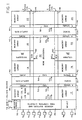
- the redundancy scheme herein is described as part of a 64K dynamic RAM (random access memory). To illustrate how the redundancy scheme interfaces with the RAM, reference is made to Figure 1 which shows the architecture of the RAM's chip.
- the RAM's memory includes 256 rows by 256 columns of cells and is divided into eight main arrays or octants 10, 12, 14, 16, 18, 20, 22 and 24. Each of the latter arrays includes 64 columns by 128 rows of memory cells.
- To access a particular cell one bit of row address information is received at each of the eight input pins AO-A7.
- the row information received at pins AO-A5 is applied to a block 30 entitled “address buffers and fuse compare circuits". Ignoring the "fuse" function for the moment, the block 30 buffers the address inputs, and for each address input, develops true and complementary address outputs A 1 and A 1 which are used to drive row decoders 32. These decoders operate to select a group of four rows of cells from the memory.
- select circuitry 34 To identify the one row which the 8 bits of address information uniquely identifies, the bits received at pins A6 and A7 are coupled to select circuitry 34.
- the latter circuitry typically selects one of the rows associated with one of the four previously selected rows.
- Sense amplifiers 35 and 35a amplify and couple the data associated with the selected row to a data output (not shown).
- the input pins AO-A7 then receive an 8 bit column address word.
- the uniquely identified column is then accessed in the manner described above except that column decoders 36 are employed rather than the row decoders 32.
- the illustrated RAM includes 16 spare rows of memory cells and 4 spare columns of memory cells.
- the spare rows are shown as 4 groups 38, 40, 42 and 44 of spare rows, each such group including four rows.
- the spare columns are shown as two groups 46 and 48 of spare columns, each such group including two columns.
- each of the spare groups of rows may replace four main rows of cells in the memory, as defined by AO-A5, and each of the spare groups of columns may replace any two main columns of cells in memory.
- the RAM includes fuse circuitry in the block 30 for retaining addresses of defective main rows and columns of cells, decoder disable circuitry 50, spare row decoders (SRD) 52, 54, 56 and 58, and spare column decoders (SCD) 60 and 62.
- the fuse circuitry in the block 30 is programmed during probe testing with addresses of defective cells and operates such that, when the input pins AO-A5 receive an address previously found to be that of a defective cell, spare select signals SI 1 and SI 2 are generated for enabling the spare row decoders 52-58 and the spare column decoders 60 and 62.
- the spare row decoder 52 accesses the four spare rows 38.
- the decoder disable circuits 50 force the signals A and A, high to inhibit the row decoders 32 from accessing the memory array 10.
- the signal SI 1 enables the spare column decoder 60 for accessing the four spare columns 46.
- the decoder disable circuits 50 disable the main column decoders 36.
- the groups 38 and 40 of spare rows can each replace 4 rows in any of the memory arrays 10, 12, 14 or 16.
- the groups 42 and 44 of spare rows can each replace four rows in any of the memory arrays 18, 20, 22 and 24.
- the groups 46 and 48 of spare columns can replace four main columns anywhere on the chip.
- the address buffer 64 may be of conventional construction for receiving an input address bit A in1 , and a reference voltage V ref . If A in1 is greater than V ref , the input is considered to be a-logical "one", the output A on lead 66 goes high, and the output A i on lead 68 remains low. Conversely, if A in1 ⁇ is less than V, ef , the input is considered to be a logical "zero", A, goes high, and A remains low.
- the signals on the leads 66 and 68 are applied as inputs to the row decoders 32 and the column decoders 36.
- a store for a defective row address comprising a pair of row fuse circuits 70 and 72, and a store for a defective column address comprising a pair of column fuse circuits 74 and 76.
- the row fuse circuit 70 receives an input identified as ECR 1 and a row select clock input identified as 0 ⁇ RS .
- ECR 1 an input identified as ECR 1
- a row select clock input identified as 0 ⁇ RS .
- an automatic memory tester senses the operability of all cells in the memory.
- a high level signal ECR 1 is applied to an internal pad on the chip for application to the row fuse circuit 70 and to other similar row fuse circuits located in the block 30 ( Figure 1).
- the row fuse circuit 70 blows an internal fuse for storing the address of the group of rows including the defective cell.
- the column fuse circuit 74 is similar to the row fuse circuit 70 except that it receives (during probe test) a signal identified as ECC 1 for storing the address of a group of columns having a defective memory cell.
- the column fuse circuitry 74 is clocked by a column select signal identified as 0cs.
- the row fuse circuit 72 and the column fuse circuit 76 are similar, respectively to circuits 70 and 74, except that the former receive probe test inputs identified as ECR 2 and ECC 2 .
- the row fuse circuit 70 may store one bit of an address of a group of defective rows anywhere on the chip.
- the row fuse circuit 72 may store another bit of an address of a group of defective rows anywhere on the chip.
- the other five buffers and fuse circuits in the block 30 store the remainder of the address.
- the column fuse circuits 74 and 76 each store a bit of an address of a group of defective columns anywhere on the chip.
- the address stored in the fuse circuitry is compared with incoming row and column addresses. If a stored address is the same as an incoming address, a group of four spare columns or rows is substituted for the defective group of columns or rows.
- the output of the row fuse circuitry 70 is coupled via switches S1 and S2 to the inputs of a comparator comprising gates 78, 80 and 82.
- the gates 78 and 80 also receive as inputs the incoming buffered addresses A and A, for comparison with the output of the fuse circuitry 70 and 74.
- the gates 78, 80 and 82 act essentially as an exclusive OR circuit such that, when the inputs A and A, match the address stored in the row fuse circuitry 70, the spare inhibit output SI 1 on lead 84 remains at a low level. If no such match occurs, the output SI 1 is pulled high.
- a simultaneous comparison occurs between the buffered inputs A and A i , and the outputs of row fuse circuit 72.
- the latter's outputs are coupled via switches S3 and S4 to another exclusive OR type comparator comprising gates 86,88 and 90.
- the gates 86 and 88 also receive the signals A i and A,. If a match occurs between the signals A, and A, and the output of the row fuse circuitry 72, a spare input output SI 2 at lead 92 remains low. If no match occurs SI 2 is pulled high.
- the spare columns can replace defective main columns anywhere on the chip, either of the signals ECC 1 and ECC 2 may go high to select a particular group of columns to be replaced by spare columns.
- the automatic memory tester may, for example, drive the signal ECC, high on locating a first defective cell and then drive the signal ECC 2 high on locating a defective cell in another column.
- the reverse sequence may also be used.
- the lead 84 is wire ORed to corresponding outputs of similar fuse circuitry associated with the other five address buffers in the block 30. Thus, if any one bit of an incoming row address does not match with a programmed fuse address, the line carrying the ORed spare inhibit signals SI 1 will be pulled high. This in turn will cause a spare row to be left unselected. If, however, all bits of the incoming address match the address programmed in the fuse circuitry, the line carrying the spare inhibit signal will remain low and a group of spare rows will be selected.
- the spare inhibit SI 2 is also wire ORed to similar output of fuse circuitry associated with the other five address buffers.
- the switches (which may be logic operated transistors) are thrown to their other positions for comparing the buffered address inputs with addresses programmed or stored in the column fuse circuits 74 and 76. If all bits of an incoming column address match the programmed fuse addresses of defective columns, the line carrying the ORed SI 1 (or S1 2 ) inhibit signals remains at a low level. If no such match occurs, that line is pulled high.
- the address of a group of rows or columns is stored and compared with the incoming address.
- two programmable addresses (both row and column) are provided for maximum flexibility in correcting defects.
- any two arbitrary groups of four rows and two columns can be replaced. If, for example, a defect crosses an address boundary, i.e., the defective rows or columns are identified by different addresses, the memory can still be repaired since any two arbitrary groups can be replaced.
- Another advantage of the illustrated arrangement is that column address inputs and row address inputs time share a single buffer and the same comparison circuitry. Hence, a reduction in circuit complexity is provided.
- a reduction in the number of fuses required in the embodiment of Figure 2 may be effected by replacing the second row and column fuse circuits 72 and 76 with A+ comparators, where A indicates the address of a defective cell stored in fuse circuits 70 or 74.
- A indicates the address of a defective cell stored in fuse circuits 70 or 74.
- the row fuse circuit 70 is associated with cell address 000000 and its fuse is blown, it may output a signal to an A+1 generator (which replaces row fuse circuit 72) for developing output signals indicative of a defective cell at address 000001.
- the number of fuses required can be halved. While only adjacent groups of cells can be fixed in this manner, the ability to correct defects on address boundaries is maintained.
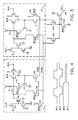
- FIG. 3 a circuit diagram is shown for the row fuse circuit 70, the column fuse circuit 74, and their common comparator.
- the row fuse circuit 72, the column fuse circuit 76, and their comparator may be similarly constructed.
- the row fuse circuit 70 is similar to the column fuse circuit 74. Hence, a description will only be given of the operation of the circuit 70, it being understood that the column fuse circuit 74 operates in a similar manner.
- the circuit 70 includes a fuse F1 which may be made of polysilicon material and which is blown during probe testing to store information indicative of the address of a defective cell.
- the circuit 70 includes transistors 94 and 98, the drain of the latter transistor being coupled to a node 100 and to the fuse F1 for carrying fuse blowing current from V cc , through the fuse F1, and to ground when the transistor 98 is turned on.
- a high level signal identified as ECR 1 will be applied to the gate of the transistor 94 when the address input A is also driven high. Consequently, the transistor 94 conducts to turn on the transistor 98, thereby providing a path for fuse blowing current through the fuse F1 and to ground through the transistor 98.
- a transistor 99 is coupled to the gate of the transistor 98 to hold the voltage there at a low level except when the signals A, and ECR 1 are high.
- waveforms are shown of four clock signals 0 ⁇ AS , 0 ⁇ AR , 0 ⁇ RS and 0cs which are applied to the fuse circuits 70 and 74 during normal operation of the memory.
- the signal BAR is initially high, as shown in Figure 4, and is applied to transistors 102 and 104 in the circuit 70, and to a transistor 106 in the circuit 74.
- the sources of transistors 102 and 106 are coupled to lines identified as "fuse” and "fuse", respectively, so as to initially precharge both lines to a high level, such as four volts when V cc is equal to 5 volts.
- a node 108 which is coupled to the transistor 104, is also pulled high.
- a grounded source transistor 110 is coupled to the node 108, wherefore the latter transistor is turned on.
- another transistor 112 coupled to the drain of the transistor 110, is also turned on.
- the voltage at the drain of transistor 112 tries to fall, but it is held at a high level by the unblown impedance of the fuse F1.
- the node 100 is also coupled to the gate of a transistor 114 whose source receives the signal BAR and whose drain is coupled to the node 108.
- the transistor 114 turns on to pull the voltage at node 108 low.
- the latter node is coupled to the fuse line via another transistor 116 whose gate receives the signal 0 ⁇ RS . Because 0 ⁇ RS is at a high level, the transistor 116 is on for coupling the low level at node 108 to the fuse line.
- the fuse line is coupled to a transistor 118 whose gate receives the signal 0 ⁇ RS and whose drain is coupled to the node 100. With 0 ⁇ RS high, the transistor 118 couples node 100 to the fuse line which remains high because of the high level at node 100. Thus, with the fuse F1 unblown, the fuse line is high and the fuse line is low.
- the fuse and fuse lines are, of course, both initially precharged to high levels as described above when the signal BAR is high.
- the signal 0 ⁇ RS is also high, thereby holding the transistor 118 on to pull the voltage at node 100 low.
- the voltage at node 100 falls no later than the signal BAR goes low. Consequently, the transistor 114 remains off.
- the off condition of the transistor 114 allows the fuse line to remain at its precharged high level.
- the fuse line is pulled low because the transistor 118 couples the fuse line to the low potential of the node 100.
- the fuse line is low and the fuse line is high.
- a comparator comprising transistors 120, 122 and 124 is coupled to the fuse and fuse lines at the gates of transistors 120 and 122.
- the drains of the latter transistors receive the incoming address bits A and A, respectively, from the address buffer. If the fuse F1 had been previously blown, the fuse line is low and the fuse line is high. Now if the input A is low and the input% is high, the transistor 122 causes a node 126 to be driven low. The low level signal at the node 126 is buffered to the output lead 128 to develop a low level spare inhibit signal (SI 1 ). Consequently, a spare row decoder is enabled for accessing a spare row of memory cells.
- the transistor 124 receives the signal 0 ⁇ AR at its gate in order to start the node 126 at low level.
- the spare inhibit signal SI 1 is driven to a high level for inhibiting the selection of a spare row.
- the fuse circuitry 74 operates in a manner similar to that described above with respect to the fuse circuitry 70 so that the spare inhibit signal SI 1 is held low when an incoming column address matches the address information associated with the fuse F2.
- circuitry comprising transistors 110, 112 and 114 and the manner in which they are clocked.
- transistors 110, 112 and 114 With the illustrated arrangement, a very simple circuit is provided for generating fuse and fuse data with no continuous consumption of D.C. current. It also allows one end of the fuse F, to be coupled to V cc for ease of fusing in N channel logic.
- the circuit also reliably senses the state of the fuse F1 even though the impedance of the fuse may change but from 100 ohms in an unblown state to 1000 ohms in its blown state. This effect is due to the fact that, because all the fuse current flows through transistors 110 and 112 when 0 ⁇ AS is high, those transistors may be sized to carry the required current to drop the potential at node 100 sufficiently for holding the transistor 114 off. Thus, even though the fuse may not blow completely, the illustrated circuit is made sensitive enough to detect a relatively small impedance change in the fuse F1.
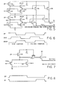
- the illustrated circuitry includes transistors 130 and 132 which receive the spare inhibit signal SI 1 , developed by the fuse and compare circuit of Figure 3. Another pair of transistors 134 and 136 receive another spare inhibit signal SI 2 developed by additional fuse and compare circuitry which may be similar to that shown in Figure 3 except that it operates on different address inputs.
- transistors 138 and 140 Coupled to the drains of transistors 130 and 134, respectively, are transistors 138 and 140 whose gates receive a precharge clock signal identified as 0p.
- the source of the transistor 138 is coupled to the gate of another transistor 142 which receives a clock signal identified as 0 ⁇ AOR .
- the source of the transistor 140 is coupled to the gate of a transistor 144 which also receives the clock signal 0 ⁇ AOR .
- clock signals 0p and 0 ⁇ AOR are shown, along with the clock address select 0 ⁇ AS to indicate the relative timing of the various clocks.
- the drain of the transistor 132 is coupled to the gates of transistors 146 and 148, the sources of which are coupled to leads 150 and 152. These leads force the address data signals A i and A, to both go high when a spare row or column is selected in order to disable the row and column decoders.
- the drain of the transistor 136 is also coupled to the gates of a pair of transistors 154 and 156 whose sources are coupled to leads 150 and 152.
- the transistors 138 and 140 are turned on by the signal 0 ⁇ p for initially precharging nodes 158 and 160 to high levels. If the signals SI 1 and SI 2 are both high (no match between an incoming address and an address of a defective cell), transistors 130 and 134 conduct to pull the voltages at nodes 158 and 160 low. When the signal 0 ⁇ AOR goes high, the drains of transistors 132 and 136 (nodes 162 and 164) remain low. Hence, transistors 146, 148, 154 and 156 remain off and the state of the signals A i and A i remains unaltered to prevent disabling the row and column decoders.
- the node 158 would have remained high and the node 162 would have been driven high when 0 ⁇ AOR came up. This would have turned transistors 146 and 148 on to drive the signals A i and A i high. Consequently, the row and column decoders would be disabled.
- Figure 1 shows an exemplary decoder which may be used in the main row and column decoders
- Figure 9 shows an exemplary decoder which may be used in the spare row decoder and the spare column decoder.
- Figure 8 illustrates clock signals 0p and 0 1 which are input to the decoders in Figures 7 and 9.
- the decoder shown therein includes address input transistors 166a-166n, each of which receives one bit of an address input. Coupled to the drains of transistors 166a-166n is another transistor 168 whose gate receives the precharge clock signal 0p. Its source is coupled by a transistor 170 to the gate of an output transistor 172.
- the transistor 168 is turned on by the signal 0p. Then, if all address inputs remain low, the high level voltage at the source of transistor 168 is coupled to the decoder's output for selecting main columns or rows of memory cells.
- the spare decoder shown in Figure 9 includes a transistor 174 for receiving a spare inhibit signal SI 1 (or S1 2 ) at its gate, a transistor receiving the clock signal 0p at its gate, and transistors 178 and 180.
- the clock signal 0p turns on the transistor 176 for precharging the drain connection (node 182) of the transistor 174. If the signal SI 1 then goes high, the node 182 and the spare decoder's output are pulled low to prevent selection of a spare row or column. If, however, the signal SI 1 goes low, the decoder's output stays high for selecting a spare row or column.
- FIG. 10 a simplified diagram of the RAM's architecture is shown to explain an alternate way of replacing defective columns of cell.
- the memory is again shown as being divided into octants 10, 12, 14, 16, 18, 20, 22 and 24.
- the top half of the figure shows a pair of memory columns C which extend through quadrants 10, 14, 18 and 22.
- Another pair of columns C+1 is adjacent the column C, and a defect D is shown which covers adjacent columns.
- the two spare columns 46 may be thought of as including portions 46a and 46b, and the two spare columns 48 may be thought of as including portions 48a and 48b.
- the defect may be cured by substituting spare column portions 48a and 48b for the entirety of main column pairs C+1.
- the main decoders are disabled when spare columns 46 and 48 are selected in order to prohibit access to any portion of the main memory array.
- a split memory array is used wherein memory columns to the left of the decoders 36 may be accessed independently of the memory columns to the right of the decoders 36.
- the defect D may be repaired by replacing the defective portion of main column pairs C in octants 10 and 14 with spare columns portions 46a and by replacing that portion of the defective main column pairs C+1 in octants 10 and 14 with spare column portions 46b.
- the operative portions of column pairs C and C+1 which reside in octants 18 and 22 are not replaced but are accessed by the main decoders.
- spare columns 48 may be eliminated.
- the memory array is shown in simplified form as having a left sector or array L associated with a plurality of main memory columns 184 and two spare columns 186.
- a right sector or array R is associated with main memory columns 188 and two spare columns 190.
- Each of the columns 184 may be thought of as a portion or extension of one of the main columns 188.
- each main column may have a left portion 188, each such portion containing half the memory cells of a full column.
- the spare columns 186 and 190 together contain the same number of memory cells as spare columns 46 in Figure 10.
- main I/O busses 192 and 194 for communicating with the main columns of the left and right arrays, respectively
- spare I/O busses 196 and 198 for communicating with the spare columns 186 and 190, respectively.
- a pair of logic operated switches 202 and 204 are included along with switch contacts 206, 208, 210 and 212, 214 and 216.
- the switch contacts are coupled to the various I/O busses as shown, and the switches 202 and 204 are coupled via sense amplifiers 218 and 220 and another logic operated switch 222 to an output latch 224.
- the column pair C may be replaced by spare columns 186 and the column pair C+1 may be replaced by spare columns 190.
- data is retrieved from the operative main columns as well as from the spare columns by the switch 204 closing with the contact 216 for accessing the spare I/O buss 198, and by the switch 202 closing with contact 208 for accessing the main I/O buss 192.
- the data thus retrieved is coupled via the sense amplifiers 218 and 220 to the switch 222 which may be logic-operated to couple the data retrieved from the spare column 190 to the output latch 224.
- switch 202 When the column pair C is addressed, the switch 202 is closed with contact 206 to access the spare I/O buss 196 and switch 204 is closed with contact 214 to access the main I/O buss 194.
- the switch 202 may close with the contact 208 for accessing the main I/0 buss 102 and th.e switch 204 may close to contact 214.
- various combinations of switch contacts causes various main and spare columns to be accessed, all without disabling the RAM's main column decoders and yet eliminating half of the spare memory cells.
- the present redundancy scheme is adapted to repair large as well as small defects which occur in the main memory cells, and is particularly well suited for repairing defects which cross an address boundary.
Landscapes
- For Increasing The Reliability Of Semiconductor Memories (AREA)
- Techniques For Improving Reliability Of Storages (AREA)
Claims (6)
dadurch gekennzeichnet, daß jeder der Adressenpuffer (64) geeignet ist, ein Eingabe-Bit, das einer Zeilenadresse, und eine Eingabe-Bit, das einer Spaltenadresse einer Hauptspeicherzelle zugeordnet ist, zu empfangen, und geeignet ist, sequentiell Ausgabedaten zu erzeugen, die der Zeilenadresse entsprechen, und Ausgabedaten, die der Spaltenadresse entsprechen,
Applications Claiming Priority (2)
| Application Number | Priority Date | Filing Date | Title |
|---|---|---|---|
| US06/194,613 US4389715A (en) | 1980-10-06 | 1980-10-06 | Redundancy scheme for a dynamic RAM |
| US194613 | 1980-10-06 |
Related Child Applications (1)
| Application Number | Title | Priority Date | Filing Date |
|---|---|---|---|
| EP85113807.3 Division-Into | 1985-10-30 |
Publications (3)
| Publication Number | Publication Date |
|---|---|
| EP0049629A2 EP0049629A2 (de) | 1982-04-14 |
| EP0049629A3 EP0049629A3 (en) | 1983-08-17 |
| EP0049629B1 true EP0049629B1 (de) | 1987-05-27 |
Family
ID=22718253
Family Applications (2)
| Application Number | Title | Priority Date | Filing Date |
|---|---|---|---|
| EP81304603A Expired EP0049629B1 (de) | 1980-10-06 | 1981-10-05 | Redundanzschema für einen dynamischen Direktzugriffspeicher |
| EP85113807A Expired EP0180212B1 (de) | 1980-10-06 | 1981-10-05 | Redundanzstruktur für einen dynamischen Speicher |
Family Applications After (1)
| Application Number | Title | Priority Date | Filing Date |
|---|---|---|---|
| EP85113807A Expired EP0180212B1 (de) | 1980-10-06 | 1981-10-05 | Redundanzstruktur für einen dynamischen Speicher |
Country Status (5)
| Country | Link |
|---|---|
| US (1) | US4389715A (de) |
| EP (2) | EP0049629B1 (de) |
| JP (1) | JPS5792500A (de) |
| CA (1) | CA1160342A (de) |
| DE (2) | DE3176222D1 (de) |
Families Citing this family (106)
| Publication number | Priority date | Publication date | Assignee | Title |
|---|---|---|---|---|
| JPS57105898A (en) * | 1980-12-23 | 1982-07-01 | Fujitsu Ltd | Field programmable element |
| JPS5868296A (ja) * | 1981-10-16 | 1983-04-23 | Nec Corp | 記憶装置 |
| JPS58137192A (ja) * | 1981-12-29 | 1983-08-15 | Fujitsu Ltd | 半導体記憶装置 |
| US4493075A (en) * | 1982-05-17 | 1985-01-08 | National Semiconductor Corporation | Self repairing bulk memory |
| GB2129585B (en) * | 1982-10-29 | 1986-03-05 | Inmos Ltd | Memory system including a faulty rom array |
| JPH0670880B2 (ja) * | 1983-01-21 | 1994-09-07 | 株式会社日立マイコンシステム | 半導体記憶装置 |
| US4556975A (en) * | 1983-02-07 | 1985-12-03 | Westinghouse Electric Corp. | Programmable redundancy circuit |
| JPS59152597A (ja) * | 1983-02-18 | 1984-08-31 | Nec Corp | メモリ回路 |
| US4534029A (en) * | 1983-03-24 | 1985-08-06 | International Business Machines Corporation | Fault alignment control system and circuits |
| US4577294A (en) * | 1983-04-18 | 1986-03-18 | Advanced Micro Devices, Inc. | Redundant memory circuit and method of programming and verifying the circuit |
| US4566102A (en) * | 1983-04-18 | 1986-01-21 | International Business Machines Corporation | Parallel-shift error reconfiguration |
| JPS60501878A (ja) * | 1983-07-14 | 1985-10-31 | アドバンスト・マイクロ・ディバイシズ・インコ−ポレ−テッド | 列冗長性回路を有するバイト幅メモリ回路 |
| US4586178A (en) * | 1983-10-06 | 1986-04-29 | Eaton Corporation | High speed redundancy processor |
| JPH0666120B2 (ja) * | 1983-11-09 | 1994-08-24 | 株式会社東芝 | 半導体記憶装置の冗長部 |
| JPH0666394B2 (ja) * | 1983-12-16 | 1994-08-24 | 富士通株式会社 | 半導体記憶装置 |
| GB2154032B (en) * | 1984-02-08 | 1988-04-20 | Inmos Ltd | A repairable memory array |
| GB2166273A (en) * | 1984-10-29 | 1986-04-30 | Thesys Memory Products Corp | Fault avoidance in semiconductor memories |
| US4670748A (en) * | 1985-08-09 | 1987-06-02 | Harris Corporation | Programmable chip select decoder |
| US4757474A (en) * | 1986-01-28 | 1988-07-12 | Fujitsu Limited | Semiconductor memory device having redundancy circuit portion |
| JPS62217498A (ja) * | 1986-03-06 | 1987-09-24 | Fujitsu Ltd | 半導体記憶装置 |
| KR890003691B1 (ko) * | 1986-08-22 | 1989-09-30 | 삼성전자 주식회사 | 블럭 열 리던던씨 회로 |
| US4837747A (en) * | 1986-11-29 | 1989-06-06 | Mitsubishi Denki Kabushiki Kaisha | Redundary circuit with a spare main decoder responsive to an address of a defective cell in a selected cell block |
| JPS63140550A (ja) * | 1986-12-01 | 1988-06-13 | Mitsubishi Electric Corp | 冗長回路用電気ヒユ−ズ |
| US4800302A (en) * | 1987-07-17 | 1989-01-24 | Trw Inc. | Redundancy system with distributed mapping |
| DE68928112T2 (de) * | 1988-03-18 | 1997-11-20 | Toshiba Kawasaki Kk | Masken-rom mit Ersatzspeicherzellen |
| US5022006A (en) * | 1988-04-01 | 1991-06-04 | International Business Machines Corporation | Semiconductor memory having bit lines with isolation circuits connected between redundant and normal memory cells |
| US5687109A (en) * | 1988-05-31 | 1997-11-11 | Micron Technology, Inc. | Integrated circuit module having on-chip surge capacitors |
| JP2776835B2 (ja) * | 1988-07-08 | 1998-07-16 | 株式会社日立製作所 | 欠陥救済用の冗長回路を有する半導体メモリ |
| US5265055A (en) * | 1988-10-07 | 1993-11-23 | Hitachi, Ltd. | Semiconductor memory having redundancy circuit |
| US5617365A (en) | 1988-10-07 | 1997-04-01 | Hitachi, Ltd. | Semiconductor device having redundancy circuit |
| JP2547633B2 (ja) * | 1989-05-09 | 1996-10-23 | 三菱電機株式会社 | 半導体記憶装置 |
| US6069814A (en) * | 1989-05-26 | 2000-05-30 | Texas Instruments Incorporated | Multiple input buffers for address bits |
| US5471427A (en) * | 1989-06-05 | 1995-11-28 | Mitsubishi Denki Kabushiki Kaisha | Circuit for repairing defective bit in semiconductor memory device and repairing method |
| JP2837433B2 (ja) * | 1989-06-05 | 1998-12-16 | 三菱電機株式会社 | 半導体記憶装置における不良ビット救済回路 |
| GB8926004D0 (en) * | 1989-11-17 | 1990-01-10 | Inmos Ltd | Repairable memory circuit |
| US5126973A (en) * | 1990-02-14 | 1992-06-30 | Texas Instruments Incorporated | Redundancy scheme for eliminating defects in a memory device |
| EP0448980B1 (de) * | 1990-03-29 | 1997-06-11 | Texas Instruments Incorporated | Vorrichtung und Verfahren für die Beseitigung von Fehlern eines Speichers |
| JP3325456B2 (ja) * | 1996-05-22 | 2002-09-17 | 株式会社アドバンテスト | メモリリペア方法ならびにそのメモリリペア方法が適用される電子ビームメモリリペア装置およびメモリ冗長回路 |
| JP2632089B2 (ja) * | 1990-06-07 | 1997-07-16 | 三菱電機株式会社 | 半導体回路装置 |
| DE69128173T2 (de) * | 1990-07-31 | 1998-05-14 | Texas Instruments Inc | Redundante Halbleiterspeicheranordnung |
| JP2632076B2 (ja) * | 1990-08-02 | 1997-07-16 | 三菱電機株式会社 | 半導体記憶装置 |
| JPH0831279B2 (ja) * | 1990-12-20 | 1996-03-27 | インターナショナル・ビジネス・マシーンズ・コーポレイション | 冗長システム |
| KR940008208B1 (ko) * | 1990-12-22 | 1994-09-08 | 삼성전자주식회사 | 반도체 메모리장치의 리던던트 장치 및 방법 |
| KR970000501B1 (en) * | 1991-04-12 | 1997-01-13 | Hyundai Electronics Ind | Semiconductor memory device with redundancy confirmative circuit |
| US5257228A (en) * | 1991-05-16 | 1993-10-26 | Texas Instruments Incorporated | Efficiency improved DRAM row redundancy circuit |
| US6026505A (en) * | 1991-10-16 | 2000-02-15 | International Business Machines Corporation | Method and apparatus for real time two dimensional redundancy allocation |
| KR950001837B1 (ko) * | 1992-07-13 | 1995-03-03 | 삼성전자주식회사 | 퓨우즈 박스를 공유하는 로우 리던던시 회로 |
| US5471479A (en) * | 1992-08-06 | 1995-11-28 | Motorola, Inc. | Arrangement for column sparing of memory |
| JPH0668700A (ja) * | 1992-08-21 | 1994-03-11 | Toshiba Corp | 半導体メモリ装置 |
| US5588115A (en) * | 1993-01-29 | 1996-12-24 | Teradyne, Inc. | Redundancy analyzer for automatic memory tester |
| GB9305801D0 (en) * | 1993-03-19 | 1993-05-05 | Deans Alexander R | Semiconductor memory system |
| US5377146A (en) * | 1993-07-23 | 1994-12-27 | Alliance Semiconductor Corporation | Hierarchical redundancy scheme for high density monolithic memories |
| JPH07122076A (ja) * | 1993-10-25 | 1995-05-12 | Mitsubishi Electric Corp | キャッシュメモリ |
| US5552740A (en) * | 1994-02-08 | 1996-09-03 | Micron Technology, Inc. | N-channel voltage regulator |
| FR2715883B1 (fr) * | 1994-02-10 | 1996-03-29 | Snecma | Procédé d'obtention d'une pièce circulaire métallique renforcée par des fibres. |
| KR0131721B1 (ko) * | 1994-06-08 | 1998-04-15 | 김주용 | 반도체 소자의 컬럼 리던던시 장치 |
| US5544113A (en) * | 1994-11-30 | 1996-08-06 | International Business Machines Corporation | Random access memory having a flexible array redundancy scheme |
| KR0174338B1 (ko) * | 1994-11-30 | 1999-04-01 | 윌리엄 티. 엘리스 | 간단하게 테스트할 수 있는 구성을 갖는 랜덤 액세스 메모리 |
| US5627786A (en) * | 1995-02-10 | 1997-05-06 | Micron Quantum Devices, Inc. | Parallel processing redundancy scheme for faster access times and lower die area |
| US6108237A (en) * | 1997-07-17 | 2000-08-22 | Micron Technology, Inc. | Fast-sensing amplifier for flash memory |
| US5642322A (en) * | 1995-05-24 | 1997-06-24 | Kawasaki Steel Corporation | Layout of semiconductor memory and content-addressable memory |
| JP3782840B2 (ja) | 1995-07-14 | 2006-06-07 | 株式会社ルネサステクノロジ | 外部記憶装置およびそのメモリアクセス制御方法 |
| KR0172844B1 (ko) * | 1995-12-11 | 1999-03-30 | 문정환 | 반도체 메모리 소자의 리페어 회로 |
| US5706292A (en) * | 1996-04-25 | 1998-01-06 | Micron Technology, Inc. | Layout for a semiconductor memory device having redundant elements |
| GB2312974A (en) * | 1996-05-10 | 1997-11-12 | Memory Corp Plc | Memory replacement |
| US5732030A (en) * | 1996-06-25 | 1998-03-24 | Texas Instruments Incorporated | Method and system for reduced column redundancy using a dual column select |
| US5754556A (en) * | 1996-07-18 | 1998-05-19 | Teradyne, Inc. | Semiconductor memory tester with hardware accelerators |
| US5781717A (en) * | 1996-09-19 | 1998-07-14 | I-Cube, Inc. | Dynamic spare column replacement memory system |
| US5996106A (en) | 1997-02-04 | 1999-11-30 | Micron Technology, Inc. | Multi bank test mode for memory devices |
| JP3796319B2 (ja) * | 1997-03-24 | 2006-07-12 | 株式会社日立製作所 | ダイナミック型ram |
| US6172935B1 (en) | 1997-04-25 | 2001-01-09 | Micron Technology, Inc. | Synchronous dynamic random access memory device |
| US5913928A (en) * | 1997-05-09 | 1999-06-22 | Micron Technology, Inc. | Data compression test mode independent of redundancy |
| WO1999018507A1 (en) * | 1997-10-08 | 1999-04-15 | Seagate Technology, Inc. | Hybrid data storage and reconstruction system and method for a data storage device |
| CA2223222C (en) * | 1997-11-28 | 2006-05-02 | Mosaid Technologies Incorporated | Data-bit redundancy for semiconductor memories |
| US6144591A (en) * | 1997-12-30 | 2000-11-07 | Mosaid Technologies Incorporated | Redundancy selection circuit for semiconductor memories |
| US6021064A (en) * | 1998-02-04 | 2000-02-01 | Vlsi Technology, Inc. | Layout for data storage circuit using shared bit line and method therefor |
| US6072713A (en) * | 1998-02-04 | 2000-06-06 | Vlsi Technology, Inc. | Data storage circuit using shared bit line and method therefor |
| US5966339A (en) * | 1998-06-02 | 1999-10-12 | International Business Machines Corporation | Programmable/reprogrammable fuse |
| US6510503B2 (en) | 1998-07-27 | 2003-01-21 | Mosaid Technologies Incorporated | High bandwidth memory interface |
| JP2001143494A (ja) * | 1999-03-19 | 2001-05-25 | Toshiba Corp | 半導体記憶装置 |
| KR100399887B1 (ko) | 1999-05-27 | 2003-09-29 | 주식회사 하이닉스반도체 | 반도체 메모리의 칼럼 구제 회로 |
| US6144593A (en) * | 1999-09-01 | 2000-11-07 | Micron Technology, Inc. | Circuit and method for a multiplexed redundancy scheme in a memory device |
| GB2370380B (en) | 2000-12-19 | 2003-12-31 | Picochip Designs Ltd | Processor architecture |
| JP2002269994A (ja) * | 2001-03-09 | 2002-09-20 | Oki Electric Ind Co Ltd | アナログ半導体メモリの冗長メモリ回路 |
| DE10119125C1 (de) * | 2001-04-19 | 2002-12-12 | Infineon Technologies Ag | Verfahren zum Vergleich der Adresse eines Speicherzugriffs mit einer bereits bekannten Adresse einer fehlerhaften Speicherzelle |
| US6744681B2 (en) * | 2001-07-24 | 2004-06-01 | Hewlett-Packard Development Company, L.P. | Fault-tolerant solid state memory |
| GB2391083B (en) * | 2002-07-19 | 2006-03-01 | Picochip Designs Ltd | Processor array |
| JP2004063023A (ja) * | 2002-07-30 | 2004-02-26 | Renesas Technology Corp | 半導体記憶装置 |
| DE10331068A1 (de) * | 2003-07-09 | 2005-02-17 | Infineon Technologies Ag | Verfahren zum Auslesen von Fehlerinformationen aus einem integrierten Baustein und integrierter Speicherbaustein |
| DE10331607B4 (de) * | 2003-07-12 | 2007-02-15 | Infineon Technologies Ag | Ausgangstreiber für eine integrierte Schaltung und Verfahren zum Ansteuern eines Ausgangstreibers |
| US7515498B2 (en) * | 2007-02-13 | 2009-04-07 | International Business Machines Corporation | Electronic fuse apparatus and methodology including addressable virtual electronic fuses |
| GB2454865B (en) | 2007-11-05 | 2012-06-13 | Picochip Designs Ltd | Power control |
| TWI375959B (en) * | 2007-11-06 | 2012-11-01 | Nat Univ Tsing Hua | Method for repairing memory and system thereof |
| JP5218228B2 (ja) * | 2008-04-23 | 2013-06-26 | 新東工業株式会社 | 搬送装置及びブラスト加工装置 |
| US7839707B2 (en) * | 2008-09-09 | 2010-11-23 | Vitesse Semiconductor Corporation | Fuses for memory repair |
| US8555141B2 (en) * | 2009-06-04 | 2013-10-08 | Lsi Corporation | Flash memory organization |
| GB2470037B (en) | 2009-05-07 | 2013-07-10 | Picochip Designs Ltd | Methods and devices for reducing interference in an uplink |
| GB2470771B (en) | 2009-06-05 | 2012-07-18 | Picochip Designs Ltd | A method and device in a communication network |
| GB2470891B (en) | 2009-06-05 | 2013-11-27 | Picochip Designs Ltd | A method and device in a communication network |
| GB2474071B (en) | 2009-10-05 | 2013-08-07 | Picochip Designs Ltd | Femtocell base station |
| GB2482869B (en) | 2010-08-16 | 2013-11-06 | Picochip Designs Ltd | Femtocell access control |
| GB2489716B (en) | 2011-04-05 | 2015-06-24 | Intel Corp | Multimode base system |
| GB2489919B (en) | 2011-04-05 | 2018-02-14 | Intel Corp | Filter |
| GB2491098B (en) | 2011-05-16 | 2015-05-20 | Intel Corp | Accessing a base station |
| US9087611B2 (en) * | 2013-03-14 | 2015-07-21 | Avago Technologies General Ip (Singapore) Pte. Ltd. | System and method for integrated circuit memory repair with binary-encoded repair control word |
| US10658067B2 (en) * | 2018-05-14 | 2020-05-19 | Micron Technology, Inc. | Managing data disturbance in a memory with asymmetric disturbance effects |
Family Cites Families (7)
| Publication number | Priority date | Publication date | Assignee | Title |
|---|---|---|---|---|
| US3969706A (en) * | 1974-10-08 | 1976-07-13 | Mostek Corporation | Dynamic random access memory misfet integrated circuit |
| US4051354A (en) * | 1975-07-03 | 1977-09-27 | Texas Instruments Incorporated | Fault-tolerant cell addressable array |
| US4047163A (en) * | 1975-07-03 | 1977-09-06 | Texas Instruments Incorporated | Fault-tolerant cell addressable array |
| US4250570B1 (en) * | 1976-07-15 | 1996-01-02 | Intel Corp | Redundant memory circuit |
| JPS5341946A (en) * | 1976-09-29 | 1978-04-15 | Hitachi Ltd | Memory system |
| US4310901A (en) * | 1979-06-11 | 1982-01-12 | Electronic Memories & Magnetics Corporation | Address mapping for memory |
| US4346459A (en) * | 1980-06-30 | 1982-08-24 | Inmos Corporation | Redundancy scheme for an MOS memory |
-
1980
- 1980-10-06 US US06/194,613 patent/US4389715A/en not_active Expired - Lifetime
-
1981
- 1981-03-03 CA CA000372145A patent/CA1160342A/en not_active Expired
- 1981-10-05 DE DE8181304603T patent/DE3176222D1/de not_active Expired
- 1981-10-05 JP JP56158571A patent/JPS5792500A/ja active Pending
- 1981-10-05 EP EP81304603A patent/EP0049629B1/de not_active Expired
- 1981-10-05 EP EP85113807A patent/EP0180212B1/de not_active Expired
- 1981-10-05 DE DE8585113807T patent/DE3177158D1/de not_active Expired - Lifetime
Non-Patent Citations (3)
| Title |
|---|
| ELECTRONICS INTERNATIONAL, vol. 53, no. 20; September 11 1980, pages 117-123; New York, US. SUD et al.: "16-K static RAM takes new route to high speed" * |
| ELECTRONICS, vol. 53, no. 6, March 13 1980, pages 115-121, New York, US. V. G. McKENNY: "Good bits swapped for bad in 64-kilobit E-PROM" * |
| IEEE INTERNATIONAL SOLID-STATE CIRCUITS CONFERENCE, vol. 24, February 1981, pages 84-85, New York, US. EATON et al.: "Memories and redundancy techniques. A 100ns 64K dynamic RAM using redundancy techniques" * |
Also Published As
| Publication number | Publication date |
|---|---|
| EP0180212A3 (en) | 1986-10-01 |
| EP0180212A2 (de) | 1986-05-07 |
| DE3177158D1 (de) | 1990-03-29 |
| EP0049629A2 (de) | 1982-04-14 |
| CA1160342A (en) | 1984-01-10 |
| JPS5792500A (en) | 1982-06-09 |
| DE3176222D1 (en) | 1987-07-02 |
| EP0049629A3 (en) | 1983-08-17 |
| US4389715A (en) | 1983-06-21 |
| EP0180212B1 (de) | 1990-02-21 |
Similar Documents
| Publication | Publication Date | Title |
|---|---|---|
| EP0180212B1 (de) | Redundanzstruktur für einen dynamischen Speicher | |
| US6281739B1 (en) | Fuse circuit and redundant decoder | |
| EP0249903B1 (de) | Halbleiterspeichergerät | |
| EP0044628B1 (de) | Redundanzschema für einen MOS-Speicher | |
| EP0034070B1 (de) | Fehler tolerierendes Speichersystem | |
| US4556975A (en) | Programmable redundancy circuit | |
| KR960002014B1 (ko) | 결점을 수리하는 용장메모리셀 어레이를 포함하는 반도체 기억장치 | |
| US5163023A (en) | Memory circuit capable of replacing a faulty column with a spare column | |
| US6249467B1 (en) | Row redundancy in a content addressable memory | |
| US4672240A (en) | Programmable redundancy circuit | |
| US5659509A (en) | Method for programming redundancy registers in a row redundancy integrated circuitry for a semiconductor memory device, and row redundancy integrated circuitry | |
| US20050041491A1 (en) | Repair apparatus and method for semiconductor memory device to be selectively programmed for wafer-level test or post package test | |
| US4639897A (en) | Priority encoded spare element decoder | |
| US4817056A (en) | Semiconductor memory device | |
| US5485424A (en) | Semiconductor memory and redundant-address writing method | |
| KR100395031B1 (ko) | 리던던트의 메모리 셀 유닛을 포함하는 집적 반도체 메모리 | |
| JPH07226100A (ja) | 半導体メモリ装置 | |
| JP2888034B2 (ja) | 半導体メモリ装置 | |
| JP2588692B2 (ja) | 冗長レジスタプログラミング方法及び列冗長集積回路 | |
| KR0161343B1 (ko) | 용장메모리셀을 가지는 반도체기억장치 | |
| JPH06111596A (ja) | メモリ | |
| US5933376A (en) | Semiconductor memory device with electrically programmable redundancy | |
| EP0503100B1 (de) | Halbleiterspeicher | |
| US6058052A (en) | Redundancy scheme providing improvements in redundant circuit access time and integrated circuit layout area | |
| US20050015654A1 (en) | Circuits and methods for repairing defects in memory devices |
Legal Events
| Date | Code | Title | Description |
|---|---|---|---|
| PUAI | Public reference made under article 153(3) epc to a published international application that has entered the european phase |
Free format text: ORIGINAL CODE: 0009012 |
|
| AK | Designated contracting states |
Designated state(s): DE FR GB NL |
|
| PUAL | Search report despatched |
Free format text: ORIGINAL CODE: 0009013 |
|
| AK | Designated contracting states |
Designated state(s): DE FR GB NL |
|
| 17P | Request for examination filed |
Effective date: 19831014 |
|
| RAP1 | Party data changed (applicant data changed or rights of an application transferred) |
Owner name: INMOS CORPORATION |
|
| GRAA | (expected) grant |
Free format text: ORIGINAL CODE: 0009210 |
|
| AK | Designated contracting states |
Kind code of ref document: B1 Designated state(s): DE FR GB NL |
|
| REF | Corresponds to: |
Ref document number: 3176222 Country of ref document: DE Date of ref document: 19870702 |
|
| ET | Fr: translation filed | ||
| PLBE | No opposition filed within time limit |
Free format text: ORIGINAL CODE: 0009261 |
|
| STAA | Information on the status of an ep patent application or granted ep patent |
Free format text: STATUS: NO OPPOSITION FILED WITHIN TIME LIMIT |
|
| 26N | No opposition filed | ||
| PGFP | Annual fee paid to national office [announced via postgrant information from national office to epo] |
Ref country code: FR Payment date: 20000918 Year of fee payment: 20 |
|
| PGFP | Annual fee paid to national office [announced via postgrant information from national office to epo] |
Ref country code: GB Payment date: 20000921 Year of fee payment: 20 |
|
| PGFP | Annual fee paid to national office [announced via postgrant information from national office to epo] |
Ref country code: NL Payment date: 20000925 Year of fee payment: 20 |
|
| PGFP | Annual fee paid to national office [announced via postgrant information from national office to epo] |
Ref country code: DE Payment date: 20001229 Year of fee payment: 20 |
|
| PG25 | Lapsed in a contracting state [announced via postgrant information from national office to epo] |
Ref country code: GB Free format text: LAPSE BECAUSE OF EXPIRATION OF PROTECTION Effective date: 20011004 |
|
| PG25 | Lapsed in a contracting state [announced via postgrant information from national office to epo] |
Ref country code: NL Free format text: LAPSE BECAUSE OF EXPIRATION OF PROTECTION Effective date: 20011005 |
|
| REG | Reference to a national code |
Ref country code: GB Ref legal event code: PE20 Effective date: 20011004 |
|
| NLV7 | Nl: ceased due to reaching the maximum lifetime of a patent |
Effective date: 20011005 |