EP0053484B1 - Verfahren zum Herstellen eines Halbleiterbauelementes - Google Patents
Verfahren zum Herstellen eines Halbleiterbauelementes Download PDFInfo
- Publication number
- EP0053484B1 EP0053484B1 EP81305592A EP81305592A EP0053484B1 EP 0053484 B1 EP0053484 B1 EP 0053484B1 EP 81305592 A EP81305592 A EP 81305592A EP 81305592 A EP81305592 A EP 81305592A EP 0053484 B1 EP0053484 B1 EP 0053484B1
- Authority
- EP
- European Patent Office
- Prior art keywords
- film
- insulating film
- opening
- resist
- semiconductor device
- Prior art date
- Legal status (The legal status is an assumption and is not a legal conclusion. Google has not performed a legal analysis and makes no representation as to the accuracy of the status listed.)
- Expired
Links
Images

Classifications
-
- H—ELECTRICITY
- H10—SEMICONDUCTOR DEVICES; ELECTRIC SOLID-STATE DEVICES NOT OTHERWISE PROVIDED FOR
- H10P—GENERIC PROCESSES OR APPARATUS FOR THE MANUFACTURE OR TREATMENT OF DEVICES COVERED BY CLASS H10
- H10P50/00—Etching of wafers, substrates or parts of devices
-
- H—ELECTRICITY
- H10—SEMICONDUCTOR DEVICES; ELECTRIC SOLID-STATE DEVICES NOT OTHERWISE PROVIDED FOR
- H10P—GENERIC PROCESSES OR APPARATUS FOR THE MANUFACTURE OR TREATMENT OF DEVICES COVERED BY CLASS H10
- H10P76/00—Manufacture or treatment of masks on semiconductor bodies, e.g. by lithography or photolithography
- H10P76/40—Manufacture or treatment of masks on semiconductor bodies, e.g. by lithography or photolithography of masks comprising inorganic materials
- H10P76/408—Manufacture or treatment of masks on semiconductor bodies, e.g. by lithography or photolithography of masks comprising inorganic materials characterised by their sizes, orientations, dispositions, behaviours or shapes
- H10P76/4085—Manufacture or treatment of masks on semiconductor bodies, e.g. by lithography or photolithography of masks comprising inorganic materials characterised by their sizes, orientations, dispositions, behaviours or shapes characterised by the processes involved to create the masks
-
- H—ELECTRICITY
- H10—SEMICONDUCTOR DEVICES; ELECTRIC SOLID-STATE DEVICES NOT OTHERWISE PROVIDED FOR
- H10P—GENERIC PROCESSES OR APPARATUS FOR THE MANUFACTURE OR TREATMENT OF DEVICES COVERED BY CLASS H10
- H10P95/00—Generic processes or apparatus for manufacture or treatments not covered by the other groups of this subclass
Definitions
- the present invention relates to a method for fabricating a semiconductor device. More particularly, the present invention relates to a method for fabricating a semiconductor device according to which adhesion of the photoresist film is improved.
- fine-processing techniques include selective etching technique utilizing plasma etching which is known as a dry process using no etching solution.
- plasma etching etching of silicon nitride, polycrystalline silicon, metal silicides or the like may be performed using the photoresist mask as an etching mask, unlike the wet process which requires an etching mask of silicon dioxide in addition to the photoresist film.
- the manufacturing method for the semiconductor devices may be simplified, and the manufacturing yield and reliability are improved.
- the adhesion between the insulating film and the photoresist film formed thereon is significantly degraded.
- the second film of Si 3 N 4 which allows selective etching on the first film of insulating material such as Si0 2
- plasma etching to form a desired pattern
- a photoresist film is formed on the exposed surface of the insulating film and an opening is formed in the insulating film by wet etching, excessive side etching occurs.
- the inner surface of the opening becomes slightly inclined, resulting in poor shape precision of the opening.
- the adhesion of the photoresist film to the insulating film is worse, the photoresist film may be separated from the insulating film during the wet etching.
- this opening is an opening for diffusion of an impurity to form a resistor
- the precision of the resistor element formed through this opening of poor precision becomes also poor.
- the characteristics of the integrated circuit device including such a resistor element also become worse. If the opening is the diffusion region of the transistor or the contact hole, the variation in the transistor characteristics becomes great. Especially when the opening is the contact hole, the junction is exposed by the opening, which may result in short-circuiting of the junction during the subsequent step of forming the electrode.
- the first and second insulating films are made of silicon oxide, silicon nitride, silicon carbide, or alumina.
- the conductor film formed on the first insulating film is made of polycrystalline silicon, a metal silicide, or a high-melting point metal.
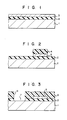
- a silicon dioxide film 2 of 400 nm (4,000 A) thickness is formed on the surface of the semiconductor silicon substrate 1. Desired elements may or may not be formed in the semiconductor substrate 1. Furthermore, an impurity of p- or n-conductivity type may or may not be implanted in the silicon dioxide film 2. A polycrystalline silicon film 3 is then deposited on the silicon dioxide film 2 to a thickness of 300 nm (3,000 A). An impurity of p- or n-conductivity type may or may not be implanted in the polycrystalline silicon film 3.
- a resist film 4 of a predetermined pattern is formed in the polycrystalline silicon film 3.
- the polycrystalline film 3 is selectively etched by plasma etching using a gas containing CF 4 and using the resist film 4 as a mask.
- a wiring layer 5 of polycrystalline silicon as shown in Fig. 2 is then formed.
- the resist film is a photoresist film of known type and may be a negative type or a positive type film.
- the entire structure is heated at a temperature above 250°C.
- the temperature for this treatment is set considering the structure of the semiconductor device. The higher the temperature, the better the treatment of the surface of the first insulating film 2 exposed to the plasma and the better the adhesion between this surface and a resist film to be formed thereover.
- too high a treating temperature results in a change in the distribution profile of the impurity.
- too high a treating temperature results in deformation of the semiconductor substrate 1. Therefore, it is generally preferable to set the treating temperature within the range of 800 to 1,000°C.
- the atmosphere for the heat treatment is selected according to the characteristics of the elements formed in advance on the semiconductor substrate, the heat treating temperature, or the like. Although it is preferable to use an inert gas such as nitrogen gas, a gas mixture of nitrogen and oxygen, for example, may also be used.
- a resist film 6 is formed on the surface of the silicon dioxide film 2 and the surface of the wiring layer 5.
- a window 8 is formed in a predetermined region of the resist film 6 so as to form an opening 7 in the silicon dioxide film 2.
- This opening 7 is for forming a resistor or an electrode.
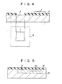
- the resist film 6 is then removed to complete the semiconductor device as shown in Fig. 4.
- the resist film is securely adhered to the silicon dioxide film. Therefore, the inner side surface of the opening 7 is formed to be substantially vertical with respect to the surface of the seniconductor substrate 1 as shown in Fig. 4., Consequently, the opening 7 can be formed with high shape precision. Since the formation of this opening does not require special etching masks other than the resist film, this step can be simplified.
- an opening 9 of the semiconductor device which is fabricated in the same manner as the embodiment described above except that the heat treat; ment is not performed, is indicated by the alternate long and short dashed line in Fig. 4. If thei heat treatment is not performed, th adhesion ofl the silicon dioxide film 2 to the resist film 6 is
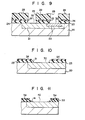
- a silicon dioxide film 23 of 400 nm (4,000 A) thickness as the first insulating film is formed on a semiconductor substrate 20 in which are formed a base region 21 and an emitter region 22 as shown in Fig. 5.
- a silicon nitride film 24 of 50 to 300 nm (500 to 3,000 A) thickness (as the second insulating film) to be the passivation film is formed on the silicon dioxide film 23.
- a photoresist film 25 is formed on the silicon nitride film 24 for forming electrodes to be connected to the base region 21 and the emitter region 22, respectively.
- openings 26 are formed in the silicon nitride film 24 by plasma etching using the photoresist film 25 as a mask.
- the photoresist film 25 is removed and the entire structure is heat treated at a temperature of 800 to 1,000°C in an atmosphere of a gas mixture of nitrogen and oxygen.
- a photoresist film 28 is then deposited on the silicon dioxide film 23 and the remaining portion of the silicon nitride film 24. Then, as shown in Fig. 8, windows 29 of smaller diameter than the openings 26 of the silicon nitride film 28 are formed in the photoresist film 28 within the area of the openings 26.
- the silicon dioxide film 23 is etched with a solution of ammonium fluoride using the photoresist film 28 as a mask. Openings 30 are formed as shown in Fig. 9. In the final step, the photoresist film 28 is removed to complete the semiconductor device.
- FIG. 11 is shown an opening 40 of a semiconductor device which is fabricated in the same manner except that the heat treatment is not performed.
- An inner side surface 41 of the opening 40 in a silicon dioxide film 33 is slightly inclined and the shape precision of the opening 40 is poor.
- the upper end of the inner side surface 41 of the opening 40 undercuts a silicon nitride film 34.
- the adhesion between the resist film and the layerforforming the opening is improved by performing heat treating after plasma etching. Therefore, a semiconductor device having an opening of high shape precision may be easily fabricated with a simplified method. In addition to this, the integration density and reliability of the semiconductor device may -also be improved.
Landscapes
- Internal Circuitry In Semiconductor Integrated Circuit Devices (AREA)
- Drying Of Semiconductors (AREA)
Claims (7)
Applications Claiming Priority (2)
| Application Number | Priority Date | Filing Date | Title |
|---|---|---|---|
| JP55169372A JPS5792833A (en) | 1980-12-01 | 1980-12-01 | Manufacture of semiconductor device |
| JP169372/80 | 1980-12-01 |
Publications (2)
| Publication Number | Publication Date |
|---|---|
| EP0053484A1 EP0053484A1 (de) | 1982-06-09 |
| EP0053484B1 true EP0053484B1 (de) | 1986-04-16 |
Family
ID=15885363
Family Applications (1)
| Application Number | Title | Priority Date | Filing Date |
|---|---|---|---|
| EP81305592A Expired EP0053484B1 (de) | 1980-12-01 | 1981-11-26 | Verfahren zum Herstellen eines Halbleiterbauelementes |
Country Status (3)
| Country | Link |
|---|---|
| EP (1) | EP0053484B1 (de) |
| JP (1) | JPS5792833A (de) |
| DE (1) | DE3174421D1 (de) |
Family Cites Families (5)
| Publication number | Priority date | Publication date | Assignee | Title |
|---|---|---|---|---|
| DE2153441A1 (de) * | 1971-10-27 | 1973-05-10 | Licentia Gmbh | Verfahren zum herstellen eines halbleiterbauelementes |
| US4075367A (en) * | 1976-03-18 | 1978-02-21 | Ncr Corporation | Semiconductor processing of silicon nitride |
| JPS52139373A (en) * | 1976-05-17 | 1977-11-21 | Hitachi Ltd | Treating method for compound semiconductor |
| JPS52139376A (en) * | 1976-05-18 | 1977-11-21 | Toshiba Corp | Production of semiconductor device |
| JPS6020901B2 (ja) * | 1978-02-10 | 1985-05-24 | 株式会社日立製作所 | 半導体装置の製造方法 |
-
1980
- 1980-12-01 JP JP55169372A patent/JPS5792833A/ja active Pending
-
1981
- 1981-11-26 DE DE8181305592T patent/DE3174421D1/de not_active Expired
- 1981-11-26 EP EP81305592A patent/EP0053484B1/de not_active Expired
Also Published As
| Publication number | Publication date |
|---|---|
| EP0053484A1 (de) | 1982-06-09 |
| DE3174421D1 (en) | 1986-05-22 |
| JPS5792833A (en) | 1982-06-09 |
Similar Documents
| Publication | Publication Date | Title |
|---|---|---|
| EP0373360A2 (de) | Verfahren und Struktur zur Herstellung einer Isolierung aus VLSI- und ULSI-Schaltungen | |
| KR100286073B1 (ko) | 측벽막을 갖는 mosfet의 제조 방법 | |
| US4292156A (en) | Method of manufacturing semiconductor devices | |
| US6440839B1 (en) | Selective air gap insulation | |
| US3986896A (en) | Method of manufacturing semiconductor devices | |
| US4551907A (en) | Process for fabricating a semiconductor device | |
| US4742025A (en) | Method of fabricating a semiconductor device including selective etching of a silicide layer | |
| KR100212689B1 (ko) | 접촉 플러그 형성방법 | |
| US4702000A (en) | Technique for elimination of polysilicon stringers in direct moat field oxide structure | |
| EP0053484B1 (de) | Verfahren zum Herstellen eines Halbleiterbauelementes | |
| JPH079930B2 (ja) | 半導体装置の製造方法 | |
| JPS6279625A (ja) | 半導体装置の製造方法 | |
| JPH0420256B2 (de) | ||
| JPS60115255A (ja) | 半導体装置の製造方法 | |
| JPS583244A (ja) | 半導体装置の製造方法 | |
| JPH01184852A (ja) | スペーサでマスクされたvlsiプロセス | |
| JPS59195859A (ja) | 半導体装置の製造方法 | |
| JPH04369854A (ja) | 半導体装置及びその製造方法 | |
| JPH028451B2 (de) | ||
| KR0134859B1 (ko) | 반도체 소자의 콘택홀 형성방법 | |
| JPS6161546B2 (de) | ||
| JPS6149439A (ja) | 半導体装置の製造方法 | |
| JPH08236475A (ja) | コンタクト窓の形成方法 | |
| JPS6130031A (ja) | 半導体装置の製造方法 | |
| JPS5994457A (ja) | 半導体装置 |
Legal Events
| Date | Code | Title | Description |
|---|---|---|---|
| PUAI | Public reference made under article 153(3) epc to a published international application that has entered the european phase |
Free format text: ORIGINAL CODE: 0009012 |
|
| 17P | Request for examination filed |
Effective date: 19811202 |
|
| AK | Designated contracting states |
Designated state(s): DE GB NL |
|
| RAP1 | Party data changed (applicant data changed or rights of an application transferred) |
Owner name: KABUSHIKI KAISHA TOSHIBA |
|
| GRAA | (expected) grant |
Free format text: ORIGINAL CODE: 0009210 |
|
| AK | Designated contracting states |
Kind code of ref document: B1 Designated state(s): DE GB NL |
|
| REF | Corresponds to: |
Ref document number: 3174421 Country of ref document: DE Date of ref document: 19860522 |
|
| PLBE | No opposition filed within time limit |
Free format text: ORIGINAL CODE: 0009261 |
|
| STAA | Information on the status of an ep patent application or granted ep patent |
Free format text: STATUS: NO OPPOSITION FILED WITHIN TIME LIMIT |
|
| 26N | No opposition filed | ||
| PGFP | Annual fee paid to national office [announced via postgrant information from national office to epo] |
Ref country code: GB Payment date: 19971117 Year of fee payment: 17 |
|
| PGFP | Annual fee paid to national office [announced via postgrant information from national office to epo] |
Ref country code: DE Payment date: 19971205 Year of fee payment: 17 |
|
| PG25 | Lapsed in a contracting state [announced via postgrant information from national office to epo] |
Ref country code: GB Free format text: LAPSE BECAUSE OF NON-PAYMENT OF DUE FEES Effective date: 19981126 |
|
| GBPC | Gb: european patent ceased through non-payment of renewal fee |
Effective date: 19981126 |
|
| PG25 | Lapsed in a contracting state [announced via postgrant information from national office to epo] |
Ref country code: DE Free format text: LAPSE BECAUSE OF NON-PAYMENT OF DUE FEES Effective date: 19990901 |
|
| PGFP | Annual fee paid to national office [announced via postgrant information from national office to epo] |
Ref country code: NL Payment date: 20001130 Year of fee payment: 20 |
|
| PG25 | Lapsed in a contracting state [announced via postgrant information from national office to epo] |
Ref country code: NL Free format text: LAPSE BECAUSE OF EXPIRATION OF PROTECTION Effective date: 20011126 |
|
| NLV7 | Nl: ceased due to reaching the maximum lifetime of a patent |
Effective date: 20011126 |