EP0053711A2 - Procédé de fabrication de structures de couches de siliciures ou de siliciures-polysilicium par pulvérisation cathodique réactive - Google Patents
Procédé de fabrication de structures de couches de siliciures ou de siliciures-polysilicium par pulvérisation cathodique réactive Download PDFInfo
- Publication number
- EP0053711A2 EP0053711A2 EP81109137A EP81109137A EP0053711A2 EP 0053711 A2 EP0053711 A2 EP 0053711A2 EP 81109137 A EP81109137 A EP 81109137A EP 81109137 A EP81109137 A EP 81109137A EP 0053711 A2 EP0053711 A2 EP 0053711A2
- Authority
- EP
- European Patent Office
- Prior art keywords
- etching
- silicides
- polysilicon
- power
- reactive sputter
- Prior art date
- Legal status (The legal status is an assumption and is not a legal conclusion. Google has not performed a legal analysis and makes no representation as to the accuracy of the status listed.)
- Granted
Links
Images
Classifications
-
- H—ELECTRICITY
- H10—SEMICONDUCTOR DEVICES; ELECTRIC SOLID-STATE DEVICES NOT OTHERWISE PROVIDED FOR
- H10P—GENERIC PROCESSES OR APPARATUS FOR THE MANUFACTURE OR TREATMENT OF DEVICES COVERED BY CLASS H10
- H10P50/00—Etching of wafers, substrates or parts of devices
- H10P50/20—Dry etching; Plasma etching; Reactive-ion etching
- H10P50/26—Dry etching; Plasma etching; Reactive-ion etching of conductive or resistive materials
- H10P50/264—Dry etching; Plasma etching; Reactive-ion etching of conductive or resistive materials by chemical means
- H10P50/266—Dry etching; Plasma etching; Reactive-ion etching of conductive or resistive materials by chemical means by vapour etching only
- H10P50/267—Dry etching; Plasma etching; Reactive-ion etching of conductive or resistive materials by chemical means by vapour etching only using plasmas
- H10P50/268—Dry etching; Plasma etching; Reactive-ion etching of conductive or resistive materials by chemical means by vapour etching only using plasmas of silicon-containing layers
Definitions
- the present patent application relates to a method for producing structures of layers consisting of silicides or double layers consisting of silicide-polysilicon on substrates containing integrated semiconductor circuits by reactive sputter etching (ion etching) with sulfur hexafluoride (SF 6 ) as an etching gas using a photoresist etching mask.
- reactive sputter etching ion etching
- sulfur hexafluoride SF 6
- anisotropic etching processes are used in the etching technology in order to ensure a dimensionally accurate structure transfer.
- Such an anisotropic etching process is described in Chemical Abstracts, Vol. 85, 1976, p. 562, left column, known.
- CF 4 Freon
- a further selectivity of polysilicon to Si0 2 and Si 3 N 4 is obtained if a gas mixture of sulfur hexafluoride (SF 6 ), chlorine and inert gas is used in the etching of silicon (see European patent application 0015403).
- SF 6 sulfur hexafluoride
- chlorine and inert gas is used in the etching of silicon.
- the etching process is carried out in two steps, first with an RF power of greater than 0.3 W / cm 2 with a high etching rate and then with an RF power of less than 0.2 W / cm 2 is etched with a lower etching rate.
- the first process step achieves strict anisotropy
- the second process step good selectivity to SiO 2 .
- the silicon substrates are folded over with metal rings, preferably made of aluminum, in order to make the etching attack more uniform.
- metal rings preferably made of aluminum
- the height of the rings must be chosen correctly. In the exemplary embodiment, 4 mm are optimal. To avoid contamination of the discs, it is advantageous to use high-purity aluminum for the rings.
- the method according to the invention is particularly suitable for the production of structures consisting of tungsten, molybdenum and tantalum silicide.
- structures consisting of tungsten, molybdenum and tantalum silicide With hexafluoride (SF 6 ) silicides of any metal content can be etched. The etching rate decreases with increasing metal content.
- SF 6 hexafluoride
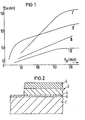
- polysilicon (curve II) already has a high etching rate at low RF powers; it is about three times as high as that of molybdenum silicide (curve III).
- the selectivity polysilicon (curve II) to Si0 2 (curve IV) is greater than 10: 1 in the second stage.
- Photoresist AZ 1450 I from Shipley
- the paint removal is in the range of the thickness of the etched double layer (approx. 500 nm).
- Figure 2 shows the example of a double layer 3 of 300 nm thick doped polysilicon 4 and an overlying 200 nm thick molybdenum silicide layer 5 with a molybdenum content of 35% that a strictly anisotropic etching process has taken place.
- the selectivity of the polysilicon layer 4 with respect to the underlying SiO 2 layer 6 is very high.
- Reference number 7 denotes the semiconductor substrate made of silicon. The paint mask has already been removed.
- the etching time for the double layer 3 consisting of polysilicon 4 and molybdenum silicide 5 is approximately 12 minutes in the method according to the invention; in known methods (e.g. etching in CF 4 plasma), the etching time is more than twice as long.
Landscapes
- Drying Of Semiconductors (AREA)
Applications Claiming Priority (2)
| Application Number | Priority Date | Filing Date | Title |
|---|---|---|---|
| DE3045922 | 1980-12-05 | ||
| DE19803045922 DE3045922A1 (de) | 1980-12-05 | 1980-12-05 | Verfahren zum herstellen von strukturen von aus siliziden oder aus silizid-polysilizium bestehenden schichten durch reaktives sputteraetzen |
Publications (3)
| Publication Number | Publication Date |
|---|---|
| EP0053711A2 true EP0053711A2 (fr) | 1982-06-16 |
| EP0053711A3 EP0053711A3 (en) | 1983-01-19 |
| EP0053711B1 EP0053711B1 (fr) | 1985-05-22 |
Family
ID=6118425
Family Applications (1)
| Application Number | Title | Priority Date | Filing Date |
|---|---|---|---|
| EP81109137A Expired EP0053711B1 (fr) | 1980-12-05 | 1981-10-28 | Procédé de fabrication de structures de couches de siliciures ou de siliciures-polysilicium par pulvérisation cathodique réactive |
Country Status (5)
| Country | Link |
|---|---|
| US (1) | US4360414A (fr) |
| EP (1) | EP0053711B1 (fr) |
| JP (1) | JPS57121232A (fr) |
| AR (1) | AR227694A1 (fr) |
| DE (1) | DE3045922A1 (fr) |
Cited By (1)
| Publication number | Priority date | Publication date | Assignee | Title |
|---|---|---|---|---|
| EP0133452A3 (en) * | 1983-05-10 | 1987-09-30 | Kabushiki Kaisha Toshiba | Reactive ion etching method |
Families Citing this family (11)
| Publication number | Priority date | Publication date | Assignee | Title |
|---|---|---|---|---|
| DE3216823A1 (de) * | 1982-05-05 | 1983-11-10 | Siemens AG, 1000 Berlin und 8000 München | Verfahren zum herstellen von strukturen von aus metallsilizid und polysilizium bestehenden doppelschichten auf integrierte halbleiterschaltungen enthaltenden substraten durch reaktives ionenaetzen |
| DE3231457A1 (de) * | 1982-08-24 | 1984-03-01 | Siemens AG, 1000 Berlin und 8000 München | Verfahren zum erzeugen von strukturen fuer integrierte halbleiterschaltungen durch reaktives ionenaetzen |
| US4462882A (en) * | 1983-01-03 | 1984-07-31 | Massachusetts Institute Of Technology | Selective etching of aluminum |
| US4470189A (en) * | 1983-05-23 | 1984-09-11 | International Business Machines Corporation | Process for making polycide structures |
| FR2555364B1 (fr) * | 1983-11-18 | 1990-02-02 | Hitachi Ltd | Procede de fabrication de connexions d'un dispositif a circuits integres a semi-conducteurs comportant en particulier un mitset |
| DE3613181C2 (de) * | 1986-04-18 | 1995-09-07 | Siemens Ag | Verfahren zum Erzeugen von Gräben mit einstellbarer Steilheit der Grabenwände in aus Silizium bestehenden Halbleitersubstraten |
| KR900003262B1 (ko) * | 1987-04-30 | 1990-05-12 | 삼성전자 주식회사 | 반도체 장치의 제조방법 |
| DE3935189A1 (de) * | 1989-10-23 | 1991-05-08 | Leybold Ag | Verfahren und vorrichtung zur behandlung von werkstuecken durch reaktives ionenaetzen |
| US5354417A (en) * | 1993-10-13 | 1994-10-11 | Applied Materials, Inc. | Etching MoSi2 using SF6, HBr and O2 |
| JPH08213475A (ja) * | 1995-02-07 | 1996-08-20 | Mitsubishi Electric Corp | 半導体装置とその製造方法 |
| RU2194335C2 (ru) * | 2000-10-26 | 2002-12-10 | Акционерное общество открытого типа "НИИ молекулярной электроники и завод "Микрон" | Способ реактивного ионно-плазменного травления слоев ta, tan, taal |
Family Cites Families (8)
| Publication number | Priority date | Publication date | Assignee | Title |
|---|---|---|---|---|
| FR2082505A5 (fr) * | 1970-03-18 | 1971-12-10 | Radiotechnique Compelec | |
| JPS5368978A (en) * | 1976-12-01 | 1978-06-19 | Mitsubishi Electric Corp | Etching method |
| DE2658448C3 (de) * | 1976-12-23 | 1979-09-20 | Deutsche Itt Industries Gmbh, 7800 Freiburg | Verfahren zum Ätzen einer auf einem Halbleiterkörper aufgebrachten Schicht aus Siliciumnitrid in einem Gasplasma |
| FR2376904A1 (fr) * | 1977-01-11 | 1978-08-04 | Alsthom Atlantique | Procede d'attaque d'une couche mince par decomposition d'un gaz dans un plasma |
| US4229247A (en) * | 1978-12-26 | 1980-10-21 | International Business Machines Corporation | Glow discharge etching process for chromium |
| US4213818A (en) * | 1979-01-04 | 1980-07-22 | Signetics Corporation | Selective plasma vapor etching process |
| US4214946A (en) * | 1979-02-21 | 1980-07-29 | International Business Machines Corporation | Selective reactive ion etching of polysilicon against SiO2 utilizing SF6 -Cl2 -inert gas etchant |
| US4283249A (en) * | 1979-05-02 | 1981-08-11 | International Business Machines Corporation | Reactive ion etching |
-
1980
- 1980-12-05 DE DE19803045922 patent/DE3045922A1/de not_active Ceased
-
1981
- 1981-10-28 EP EP81109137A patent/EP0053711B1/fr not_active Expired
- 1981-11-19 US US06/322,887 patent/US4360414A/en not_active Expired - Fee Related
- 1981-11-30 AR AR287640A patent/AR227694A1/es active
- 1981-12-04 JP JP56195498A patent/JPS57121232A/ja active Pending
Cited By (1)
| Publication number | Priority date | Publication date | Assignee | Title |
|---|---|---|---|---|
| EP0133452A3 (en) * | 1983-05-10 | 1987-09-30 | Kabushiki Kaisha Toshiba | Reactive ion etching method |
Also Published As
| Publication number | Publication date |
|---|---|
| JPS57121232A (en) | 1982-07-28 |
| EP0053711B1 (fr) | 1985-05-22 |
| US4360414A (en) | 1982-11-23 |
| DE3045922A1 (de) | 1982-07-08 |
| AR227694A1 (es) | 1982-11-30 |
| EP0053711A3 (en) | 1983-01-19 |
Similar Documents
| Publication | Publication Date | Title |
|---|---|---|
| DE68928291T2 (de) | Veraschungsverfahren zum Entfernen einer organischen Schicht auf einer Halbleiteranordnung während ihrer Herstellung | |
| DE112018005569B4 (de) | Verfahren zum bilden eines dünnschichtstapels aus strukturierungsmaterial mit metallhaltiger deckschicht für erhöhte empfindlichkeit in der extrem-ultraviolett- (euv-) lithografie | |
| EP0010596B1 (fr) | Méthode de formation d'ouvertures dans des masques pour la production de circuits semiconducteurs | |
| EP1444724B1 (fr) | Procede de structuration photolithographique au moyen d'une couche masque dure, de durete analogue au diamant, obtenue par depot assiste au plasma | |
| DE2754396C2 (fr) | ||
| DE3841588C2 (fr) | ||
| DE19805076C2 (de) | Verfahren zum Herstellen von Halbleiterbauelementen mit einem vertikalen Feldeffekttransistor | |
| DE3856022T2 (de) | Selektives Ätzen dünner Schichten | |
| DE69724192T2 (de) | Verfahren zum Ätzen von Polyzidstrukturen | |
| DE68928826T2 (de) | Reaktives Ionenätzen von Silicium enthaltenden Materialien mittels Bromwasserstoff | |
| EP0008359B1 (fr) | Procédé de fabrication d'une structure à couches minces | |
| DE69901657T2 (de) | Herstellungsverfahren für selbstjustierende lokale Zwischenverbindung | |
| EP0094528A2 (fr) | Procédé pour la fabrication de structures à double couche comportant du silicide de métal et du polysilicium sur des substrats comportant des circuits intégrés par attaque chimique par ions réactifs | |
| DE4142469B4 (de) | Verfahren zur Erzeugung und zur Entfernung von temporären Siliziumdioxid-Strukturen | |
| EP0013711B1 (fr) | Procédé de décapage des couches de chrome | |
| EP0053711B1 (fr) | Procédé de fabrication de structures de couches de siliciures ou de siliciures-polysilicium par pulvérisation cathodique réactive | |
| DE2930293A1 (de) | Aetzverfahren bei der herstellung eines gegenstandes | |
| DE69130787T2 (de) | Ätzverfahren für eine leitende Doppelschicht-Struktur | |
| EP0111086A2 (fr) | Procédé pour la fabrication de structures à dimensions sub-micrométriques et application de ce procédé pour la fabrication de régions d'isolation diélectrique profondes à largeur sub-micrométrique dans un corps semi-conducteur | |
| DE3706127A1 (de) | Diskontinuierliches aetzverfahren | |
| EP0126969B1 (fr) | Procédé pour la formation de structures comportant des siliciures métalliques, en particulier en siliciure polysilicium, pour circuits intégrés à semi-conducteurs par attaque par ions réactifs | |
| DE112006000811B4 (de) | Ätzprozess für CD-Reduzierung eines ARC-Materials | |
| EP0012863A2 (fr) | Procédé de fabrication de dispositifs semi-conducteurs à capacitance parasitaire réduite | |
| DE19852256A1 (de) | Verfahren zum Ätzen von Platin | |
| DE4446850A1 (de) | Verfahren zur Herstellung eines Transistors für eine Halbleitervorrichtung |
Legal Events
| Date | Code | Title | Description |
|---|---|---|---|
| PUAI | Public reference made under article 153(3) epc to a published international application that has entered the european phase |
Free format text: ORIGINAL CODE: 0009012 |
|
| 17P | Request for examination filed |
Effective date: 19811028 |
|
| AK | Designated contracting states |
Designated state(s): FR GB |
|
| PUAL | Search report despatched |
Free format text: ORIGINAL CODE: 0009013 |
|
| AK | Designated contracting states |
Designated state(s): FR GB |
|
| GRAA | (expected) grant |
Free format text: ORIGINAL CODE: 0009210 |
|
| AK | Designated contracting states |
Designated state(s): FR GB |
|
| ET | Fr: translation filed | ||
| PLBE | No opposition filed within time limit |
Free format text: ORIGINAL CODE: 0009261 |
|
| STAA | Information on the status of an ep patent application or granted ep patent |
Free format text: STATUS: NO OPPOSITION FILED WITHIN TIME LIMIT |
|
| 26N | No opposition filed | ||
| PG25 | Lapsed in a contracting state [announced via postgrant information from national office to epo] |
Ref country code: GB Effective date: 19881028 |
|
| PG25 | Lapsed in a contracting state [announced via postgrant information from national office to epo] |
Ref country code: FR Free format text: LAPSE BECAUSE OF NON-PAYMENT OF DUE FEES Effective date: 19890630 |
|
| GBPC | Gb: european patent ceased through non-payment of renewal fee | ||
| REG | Reference to a national code |
Ref country code: FR Ref legal event code: ST |