EP0055557A2 - Dispositif de mémoire non-volatile à semiconducteur - Google Patents
Dispositif de mémoire non-volatile à semiconducteur Download PDFInfo
- Publication number
- EP0055557A2 EP0055557A2 EP81305935A EP81305935A EP0055557A2 EP 0055557 A2 EP0055557 A2 EP 0055557A2 EP 81305935 A EP81305935 A EP 81305935A EP 81305935 A EP81305935 A EP 81305935A EP 0055557 A2 EP0055557 A2 EP 0055557A2
- Authority
- EP
- European Patent Office
- Prior art keywords
- gate
- floating
- control gate
- control
- semiconductor substrate
- Prior art date
- Legal status (The legal status is an assumption and is not a legal conclusion. Google has not performed a legal analysis and makes no representation as to the accuracy of the status listed.)
- Granted
Links
Images


Classifications
-
- H—ELECTRICITY
- H10—SEMICONDUCTOR DEVICES; ELECTRIC SOLID-STATE DEVICES NOT OTHERWISE PROVIDED FOR
- H10D—INORGANIC ELECTRIC SEMICONDUCTOR DEVICES
- H10D30/00—Field-effect transistors [FET]
- H10D30/60—Insulated-gate field-effect transistors [IGFET]
- H10D30/68—Floating-gate IGFETs
- H10D30/681—Floating-gate IGFETs having only two programming levels
- H10D30/684—Floating-gate IGFETs having only two programming levels programmed by hot carrier injection
- H10D30/686—Floating-gate IGFETs having only two programming levels programmed by hot carrier injection using hot carriers produced by avalanche breakdown of PN junctions, e.g. floating gate avalanche injection MOS [FAMOS]
-
- G—PHYSICS
- G11—INFORMATION STORAGE
- G11C—STATIC STORES
- G11C16/00—Erasable programmable read-only memories
- G11C16/02—Erasable programmable read-only memories electrically programmable
- G11C16/04—Erasable programmable read-only memories electrically programmable using variable threshold transistors, e.g. FAMOS
- G11C16/0408—Erasable programmable read-only memories electrically programmable using variable threshold transistors, e.g. FAMOS comprising cells containing floating gate transistors
- G11C16/0416—Erasable programmable read-only memories electrically programmable using variable threshold transistors, e.g. FAMOS comprising cells containing floating gate transistors comprising cells containing a single floating gate transistor and no select transistor, e.g. UV EPROM
Definitions
- the present invention relates to a nonvolatile semiconductor memory device and, more particularly, to a nonvolatile semiconductor memory device of a floating-gate type.
- a floating-gate type nonvolatile semiconductor memory device comprises two gates: a floating-gate and a control gate.
- a floating-gate In an N-channel device, for example, accumulation of electrons in the floating-gate results in a high threshold value, while expulsion of electrons from the floating-gate results in a low threshold value.
- Such two states correspond to the information "1" and "0".
- Most of the floating-gate type devices use the tunnel effect for both the write and erase operation.
- Even a FAMOS (Floating-Gate Avalanche-Injection MOS) device which is a kind of floating-gate type device. uses the tunnel effect for the erase operation. In this case, however.
- the insulating layer such as silicon dioxide (Si0 2 ) built between the floating-gate and the control gate would have to be thin enough to allow carriers to be tunneled therethrough.
- the thickness of the 0 insulating layer of Si0 2 would have to be about 30 A, which is difficult to manufacture.
- the insulating layer can be thick, but this would necessitate the application of a high voltage to the control gate, which would result in electrostatic destruction of the insulating layer.
- an object of the present invention to provide a nonvolatile semiconductor memory device which ensures stable properties in the insulating layer built between the floating-gate and the control gate and which reduces the load voltage of the insulating layer.
- a nonvolatile semiconductor memory device comprising: a semiconductor substrate of a first conductivity type; two impurity diffusion regions of a second conductivity type formed in the semiconductor substrate and apart from each other; a floating-gate formed above the semiconductor substrate and between the two impurity diffusion regions, the floating-gate being insulated from the semiconductor substrate, the floating-gate comprising first and second conductive regions having a conductivity type opposite to each other; a first control gate formed above the first conductive region of the floating-gate, the first control gate being insulated therefrom; and a second control gate formed above the second conductive region of the floating--gate, the second control gate being insulated therefrom.
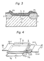
- 1 is a P -type monocrystalline substrate; 2 is a field insulating layer which is, for example, relatively thick silicon dioxide (Si0 2 ); and 3 and 4 are insulating layers which are, for example, relatively thin silicon dioxide (Si0 2 ).
- the field insulating layer 2 defines a field area, while the area in which the field insulating layer 2 is not present defines an active area.
- a floating-gate FG of polycrystalline silicon is formed on the active area and is insulated from the substrate 1 by the insulating layer 3. Further, a control gate CG is formed above the floating-gate FG and is insulated therefrom by the insulating layer 4.
- CH is a channel region in the active area under the floating-gate FG.
- S and D are a source region and a drain region, respectively, which are formed by N +- type impurity diffusion regions.
- T S ' TD, and T G are a source electrode, a drain electrode and a gate electrode, respectively.
- the write operation of the device as illustrated in Figs. 1, 2, and 3 will now be explained.
- the write operation is performed by making use of avalanche breakdown. That is, the potential of the drain electrode T D is caused to be high, so as to cause the avalanche breakdown in the vicinity of the drain junction.
- some of the hot carriers such as hot electrons due to the avalanche breakdown clear an energy barrier built between the substrate 1 and the insulating layer 3 and reach the floating-gate FG.
- such an energy barrier is about 3 eV between silicon and silicon dioxide.
- the floating-gate FG is charged and, accordingly, the write operation is completed.
- the erase operation of the device as illustrated in Figs. 1, 2, and 3 uses the tunnel effect. That is, the potential of the drain electrode T D is caused to be high, and, in addition, the potential of the gate electrode T G is caused to be low (zero), so as to expel electrons from the floating-gate FG to the control gate CG.
- the insulating layer 4 built between the floating-gate FG and the control gate CG must be so thin as to tunnel electrons therethrough.
- it is difficult to manufacture with high accuracy such a thin insulating layer, for example, 0 about 30 A thick silicon dioxide (SiO 2 ). Therefore, the erase characteristics of this FAMOS device are dependent upon the unstable properties of the insulating layer 4.
- the insulating layer 4 can be made thick so as to stabilize the layer 4; however, this would necessitates the application of a higher voltage to the control gate CG, which invites electrostatic destruction of the insulating layer 4.
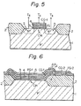
- Fig. 4 is a perspective view illustrating an embodiment of the FAMOS device according to the present invention
- Figs. 5 and 6 are cross-sectional views taken along the lines V-V and the lines VI-VI, respectively. of Fig. 4.
- Figs. 4, 5, and 6 the elements which are the same as those of Figs. 1, 2, and 3 are denoted by the same references.
- the iloating-gate FG is divided into two regions: an N-type conductive region FG-1 and a P -type conductive region F-2. Accordingly, a P + N junction is formed at the boundary between the regions FG-1 and FG-2.
- a control gate CG-1 which corresponds to the control gate CG of the device of Fig. 1
- another control gate CG-2 is provider.
- the control gate CG-1 is placed above the N-type conductive region FG-1 of the floating-gate FG, while the control cate CG-2 is placed above the P +- type conductive region 'G-2 of the floating-gate FG.
- control gate CG-2 is placed above the part of the control gate CG-1.
- edge of the control gate CG- is placed at the distance ⁇ X j shifted from the boundary between the .regions FG-1 and FG-2 on the side of the region FG-1.
- the difference in potential between the control gates CG-1 and CG-2 car induce a strong electric field within the distance ⁇ X j due to the capacitive coupling between the two control J gate CG-1 and CG-2, which performs the erase operation.
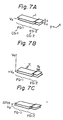
- Figs. 7A, 7B, and 7C are energy band diagrams of the floating-gate FG of Fig. 4 for explaining the write operation of the device of Fig. 4.
- an upper face indicates a conduction band E C
- a lower face indicates a valence band E V
- the control gates CG-1 and CG-2 are placed on the front side and the substrate 1 is placed on the back side.
- Fig. 7A which shows the equilibrium state in which no carriers are injected into the floating-gate FG
- the Fermi-levels of the regions FG-1 and FG-2 are consistent with the Fermi-level of the control gates CG-1 and CG-2, which is zero (V 0 ).
- the floating-gate FG when the potentials applied to the control gates CG-1 and CG-2 return to zero, the floating-gate FG consists of an enhanced concentration of electrons, that is, accumulation of electrons, due to the capacitive coupling between the floating-gate FG and the control gate CG-1.
- the Fermi-level of the floating-gate FG is reduced by 6Vth and, accordingly, a threshold value V th of the device is increased by ⁇ V th .
- Figs. 8A, 8B, and 8C are energy band diagrams of the floating-gate FG of Fig. 4 for explaining the erase operation of the device of Fig. 4.
- the application of a positive bias voltage V G to only the control gate CG-1 with the control gate CG-2 grounded causes a strong electric field in the P + N junction of the regions FG-1 and FG-2, as indicated by an arrow Z 1 , since the distance ⁇ X j is very small.
- the N-type conductive region FG-1 is insulated from the control gate CG-1 and the substrate 1
- electrons injected due to the avalanche breakdown and electrons generated from the grown depletion region of the floating-gate FG are accumulated in the region FG-1 due to the capacitive coupling between the control gate CG-1 and the N-type conductive region FG-1. Therefore, due to the presence of such a strong electric field, avalanche breakdown takes place within the floating-gate FG.
- hot electrons and hot holes are injected into both the regions FG-1 and FG-2 and, in addition, some of such electrons are expelled through the insulating layer 4 to the control gate CG-1 to which a positive bias voltage is applied.
- Fig. 8B shows the state in which a definite time passes on the condition that a positive bias voltage V G is applied to the control gate CG-1. That is, the N-type conductive region FG-1 is in a state where electrons are accumulated therein on the side of the control gate CG-1 and, in addition, the P + -type conductive region FG-2 is in a state where holes are accumulated therein on the side of the control gate CG-2. This is due to the generation of electron-hole pairs near the P N junction and in the depletion region within the N-type conductive region FG-2. In this case, the potential (Fermi-level) of the floating--gate FG is determined by the ratio of the capacitance of the control gate CG-1 to that of the control gate CG-2.
- ⁇ V th ' which is the potential (Fermi-level) of the floating-gate FG, is smaller than the value ⁇ V th in Fig. 7C. Note that the difference between the values ⁇ V th and ⁇ V th ' is due to the fact that some of the electrons are expelled through the insulating layer 4 to the control gate CG-1 as explained above.
- the nonvolatile semiconductor memory device is advantageous, as compared with the conventional device, in that the properties of the insulating layer built between the floating-gate and the control gate can be stable and, in addition, the load voltage of the insulating layer can be reduced.
Landscapes
- Engineering & Computer Science (AREA)
- Microelectronics & Electronic Packaging (AREA)
- Non-Volatile Memory (AREA)
- Semiconductor Memories (AREA)
Applications Claiming Priority (2)
| Application Number | Priority Date | Filing Date | Title |
|---|---|---|---|
| JP185336/80 | 1980-12-29 | ||
| JP55185336A JPS6059750B2 (ja) | 1980-12-29 | 1980-12-29 | 不揮発性半導体記憶装置 |
Publications (3)
| Publication Number | Publication Date |
|---|---|
| EP0055557A2 true EP0055557A2 (fr) | 1982-07-07 |
| EP0055557A3 EP0055557A3 (en) | 1984-06-06 |
| EP0055557B1 EP0055557B1 (fr) | 1987-11-25 |
Family
ID=16169014
Family Applications (1)
| Application Number | Title | Priority Date | Filing Date |
|---|---|---|---|
| EP81305935A Expired EP0055557B1 (fr) | 1980-12-29 | 1981-12-17 | Dispositif de mémoire non-volatile à semiconducteur |
Country Status (4)
| Country | Link |
|---|---|
| US (1) | US4462089A (fr) |
| EP (1) | EP0055557B1 (fr) |
| JP (1) | JPS6059750B2 (fr) |
| DE (1) | DE3176549D1 (fr) |
Families Citing this family (14)
| Publication number | Priority date | Publication date | Assignee | Title |
|---|---|---|---|---|
| JPS61131486A (ja) * | 1984-11-29 | 1986-06-19 | Res Dev Corp Of Japan | 半導体不揮発性メモリ |
| JPS63249375A (ja) * | 1987-04-06 | 1988-10-17 | Oki Electric Ind Co Ltd | 半導体記憶装置のデ−タ消去方法 |
| DE69133003T2 (de) * | 1990-01-22 | 2002-12-12 | Silicon Storage Technology, Inc. | Nichtflüchtige elektrisch veränderbare eintransistor-halbleiterspeicheranordnung mit rekristallisiertem schwebendem gate |
| US5202850A (en) * | 1990-01-22 | 1993-04-13 | Silicon Storage Technology, Inc. | Single transistor non-volatile electrically alterable semiconductor memory device with a re-crystallized floating gate |
| US5572054A (en) * | 1990-01-22 | 1996-11-05 | Silicon Storage Technology, Inc. | Method of operating a single transistor non-volatile electrically alterable semiconductor memory device |
| US5067108A (en) * | 1990-01-22 | 1991-11-19 | Silicon Storage Technology, Inc. | Single transistor non-volatile electrically alterable semiconductor memory device with a re-crystallized floating gate |
| JP3375087B2 (ja) * | 1991-10-21 | 2003-02-10 | ローム株式会社 | 半導体記憶装置およびその記憶情報読出方法 |
| US5479368A (en) * | 1993-09-30 | 1995-12-26 | Cirrus Logic, Inc. | Spacer flash cell device with vertically oriented floating gate |
| US5640031A (en) * | 1993-09-30 | 1997-06-17 | Keshtbod; Parviz | Spacer flash cell process |
| US5455791A (en) * | 1994-06-01 | 1995-10-03 | Zaleski; Andrzei | Method for erasing data in EEPROM devices on SOI substrates and device therefor |
| JP2846822B2 (ja) * | 1994-11-28 | 1999-01-13 | モトローラ株式会社 | 2層フローティングゲート構造のマルチビット対応セルを有する不揮発性メモリ及びそのプログラム方法 |
| EP0843360A1 (fr) * | 1996-11-15 | 1998-05-20 | Hitachi Europe Limited | Dispositif de mémoire |
| US6753568B1 (en) | 1996-11-15 | 2004-06-22 | Hitachi, Ltd. | Memory device |
| US6121088A (en) * | 1998-09-17 | 2000-09-19 | Taiwan Semiconductor Manufacturing Company | Method of manufacture of undoped polysilicon as the floating-gate of a split-gate flash cell |
Family Cites Families (1)
| Publication number | Priority date | Publication date | Assignee | Title |
|---|---|---|---|---|
| US4099196A (en) * | 1977-06-29 | 1978-07-04 | Intel Corporation | Triple layer polysilicon cell |
-
1980
- 1980-12-29 JP JP55185336A patent/JPS6059750B2/ja not_active Expired
-
1981
- 1981-12-16 US US06/331,286 patent/US4462089A/en not_active Expired - Fee Related
- 1981-12-17 EP EP81305935A patent/EP0055557B1/fr not_active Expired
- 1981-12-17 DE DE8181305935T patent/DE3176549D1/de not_active Expired
Also Published As
| Publication number | Publication date |
|---|---|
| DE3176549D1 (en) | 1988-01-07 |
| JPS57112077A (en) | 1982-07-12 |
| JPS6059750B2 (ja) | 1985-12-26 |
| EP0055557A3 (en) | 1984-06-06 |
| US4462089A (en) | 1984-07-24 |
| EP0055557B1 (fr) | 1987-11-25 |
Similar Documents
| Publication | Publication Date | Title |
|---|---|---|
| US4016588A (en) | Non-volatile semiconductor memory device | |
| US3984822A (en) | Double polycrystalline silicon gate memory device | |
| US4622656A (en) | Non-volatile semiconductor memory | |
| US4250569A (en) | Semiconductor memory device | |
| US4412311A (en) | Storage cell for nonvolatile electrically alterable memory | |
| US4953928A (en) | MOS device for long-term learning | |
| US3996657A (en) | Double polycrystalline silicon gate memory device | |
| US5301150A (en) | Flash erasable single poly EPROM device | |
| US4616340A (en) | Non-volatile semiconductor memory | |
| US5231299A (en) | Structure and fabrication method for EEPROM memory cell with selective channel implants | |
| JP2555027B2 (ja) | 半導体記憶装置 | |
| US3836992A (en) | Electrically erasable floating gate fet memory cell | |
| EP0055557A2 (fr) | Dispositif de mémoire non-volatile à semiconducteur | |
| US4377756A (en) | Substrate bias circuit | |
| US3469155A (en) | Punch-through means integrated with mos type devices for protection against insulation layer breakdown | |
| US4665418A (en) | Semiconductor memory device | |
| US20010002052A1 (en) | Floating gate memory with substrate band-to-band tunneling induced hot electron injection | |
| US4454524A (en) | Device having implantation for controlling gate parasitic action | |
| US4019198A (en) | Non-volatile semiconductor memory device | |
| JPS5929155B2 (ja) | 半導体記憶装置 | |
| US4084108A (en) | Integrated circuit device | |
| US4794433A (en) | Non-volatile semiconductor memory with non-uniform gate insulator | |
| US3774087A (en) | Memory elements | |
| JPH0424969A (ja) | 半導体記憶装置 | |
| EP0383210A1 (fr) | Dispositif à transfert de charge réalisant une grande efficacité de transfert de charge sans sacrifier la dynamique du signal de sortie |
Legal Events
| Date | Code | Title | Description |
|---|---|---|---|
| PUAI | Public reference made under article 153(3) epc to a published international application that has entered the european phase |
Free format text: ORIGINAL CODE: 0009012 |
|
| AK | Designated contracting states |
Designated state(s): DE FR GB NL |
|
| PUAL | Search report despatched |
Free format text: ORIGINAL CODE: 0009013 |
|
| AK | Designated contracting states |
Designated state(s): DE FR GB NL |
|
| AK | Designated contracting states |
Designated state(s): DE FR GB NL |
|
| 17P | Request for examination filed |
Effective date: 19840831 |
|
| GRAA | (expected) grant |
Free format text: ORIGINAL CODE: 0009210 |
|
| AK | Designated contracting states |
Kind code of ref document: B1 Designated state(s): DE FR GB NL |
|
| PG25 | Lapsed in a contracting state [announced via postgrant information from national office to epo] |
Ref country code: NL Effective date: 19871125 |
|
| REF | Corresponds to: |
Ref document number: 3176549 Country of ref document: DE Date of ref document: 19880107 |
|
| ET | Fr: translation filed | ||
| NLV1 | Nl: lapsed or annulled due to failure to fulfill the requirements of art. 29p and 29m of the patents act | ||
| PLBE | No opposition filed within time limit |
Free format text: ORIGINAL CODE: 0009261 |
|
| STAA | Information on the status of an ep patent application or granted ep patent |
Free format text: STATUS: NO OPPOSITION FILED WITHIN TIME LIMIT |
|
| 26N | No opposition filed | ||
| PGFP | Annual fee paid to national office [announced via postgrant information from national office to epo] |
Ref country code: GB Payment date: 19901210 Year of fee payment: 10 |
|
| PGFP | Annual fee paid to national office [announced via postgrant information from national office to epo] |
Ref country code: FR Payment date: 19901221 Year of fee payment: 10 |
|
| PGFP | Annual fee paid to national office [announced via postgrant information from national office to epo] |
Ref country code: DE Payment date: 19910222 Year of fee payment: 10 |
|
| PG25 | Lapsed in a contracting state [announced via postgrant information from national office to epo] |
Ref country code: GB Effective date: 19911217 |
|
| GBPC | Gb: european patent ceased through non-payment of renewal fee | ||
| PG25 | Lapsed in a contracting state [announced via postgrant information from national office to epo] |
Ref country code: FR Effective date: 19920831 |
|
| PG25 | Lapsed in a contracting state [announced via postgrant information from national office to epo] |
Ref country code: DE Effective date: 19920901 |
|
| REG | Reference to a national code |
Ref country code: FR Ref legal event code: ST |