EP0070737A2 - Halbleiteranordnung mit einer Elektrode und Verfahren zu deren Herstellung - Google Patents
Halbleiteranordnung mit einer Elektrode und Verfahren zu deren Herstellung Download PDFInfo
- Publication number
- EP0070737A2 EP0070737A2 EP82303828A EP82303828A EP0070737A2 EP 0070737 A2 EP0070737 A2 EP 0070737A2 EP 82303828 A EP82303828 A EP 82303828A EP 82303828 A EP82303828 A EP 82303828A EP 0070737 A2 EP0070737 A2 EP 0070737A2
- Authority
- EP
- European Patent Office
- Prior art keywords
- contact electrode
- insulating layer
- conductor line
- polycrystalline silicon
- layer
- Prior art date
- Legal status (The legal status is an assumption and is not a legal conclusion. Google has not performed a legal analysis and makes no representation as to the accuracy of the status listed.)
- Granted
Links
Images


Classifications
-
- H—ELECTRICITY
- H10—SEMICONDUCTOR DEVICES; ELECTRIC SOLID-STATE DEVICES NOT OTHERWISE PROVIDED FOR
- H10W—GENERIC PACKAGES, INTERCONNECTIONS, CONNECTORS OR OTHER CONSTRUCTIONAL DETAILS OF DEVICES COVERED BY CLASS H10
- H10W20/00—Interconnections in chips, wafers or substrates
- H10W20/01—Manufacture or treatment
- H10W20/031—Manufacture or treatment of conductive parts of the interconnections
- H10W20/062—Manufacture or treatment of conductive parts of the interconnections by smoothing of conductive parts, e.g. by planarisation
-
- H—ELECTRICITY
- H10—SEMICONDUCTOR DEVICES; ELECTRIC SOLID-STATE DEVICES NOT OTHERWISE PROVIDED FOR
- H10W—GENERIC PACKAGES, INTERCONNECTIONS, CONNECTORS OR OTHER CONSTRUCTIONAL DETAILS OF DEVICES COVERED BY CLASS H10
- H10W20/00—Interconnections in chips, wafers or substrates
- H10W20/01—Manufacture or treatment
- H10W20/031—Manufacture or treatment of conductive parts of the interconnections
- H10W20/056—Manufacture or treatment of conductive parts of the interconnections by filling conductive material into holes, grooves or trenches
- H10W20/058—Manufacture or treatment of conductive parts of the interconnections by filling conductive material into holes, grooves or trenches by depositing on sacrificial masks, e.g. using lift-off
-
- H—ELECTRICITY
- H10—SEMICONDUCTOR DEVICES; ELECTRIC SOLID-STATE DEVICES NOT OTHERWISE PROVIDED FOR
- H10W—GENERIC PACKAGES, INTERCONNECTIONS, CONNECTORS OR OTHER CONSTRUCTIONAL DETAILS OF DEVICES COVERED BY CLASS H10
- H10W20/00—Interconnections in chips, wafers or substrates
- H10W20/40—Interconnections external to wafers or substrates, e.g. back-end-of-line [BEOL] metallisations or vias connecting to gate electrodes
Definitions
- the present invention relates to a semiconductor device and a method for producing the same. More particularly, it relates to an interconnection structure in a semiconductor device, such as an integrated circuit (IC) device or a large-scale integration (LSI) device.
- IC integrated circuit
- LSI large-scale integration
- the conductor pattern comprises conductor lines (i.e., wirings) lying on an insulating layer of, e.g., phosphosilicate glass (PSG) or silicon dioxide (Si0 2 ) and making contact through small apertures (i.e., contact holes) in the insulating layer with the underlying device portion (e.g., a portion of the semiconductor substrate) or with the other,underlyingconductor line.
- conductor lines i.e., wirings
- PSG phosphosilicate glass
- Si0 2 silicon dioxide
- a conductive layer e.g., an aluminum layer
- a conductor pattern i.e. a desired pattern of conductor lines
- an insulating layer 1 (e.g., PSG) formed on semiconductor substrate 2 (e.g., a silicon wafer) is selectively etched by a conventional photoetching method using photoresist layer 3 to form contact hole 4.
- conductive material e.g., aluminum
- photoresist layer 3 and conductive layer 5b are simultaneously removed with a suitable solvent. This removal process is referred to as the lift off process.
- Wedge gap 6 (Fig. 3) is formed between contact electrode 5a and the side of insulating layer 1.
- Fig. 3 is formed between contact electrode 5a and the side of insulating layer 1.
- a semiconductor device comprises an insulating layer
- a conductor line is formed without a break or a thin portion.
- a method of producing a semiconductor device comprises the steps of forming an insulating layer on a semiconductor substrate or a conductor line; opening a contact hole in the insulating layer ; forming a contact electrode in the contact hole; and forming a conductor line on the contact electrode and insulating layer and is characterised in that the method further comprises the steps of filling a gap between the contact electrode and the side of the insulating layer with polycrystàline silicon prior to the formation of the conductor line; and alloying the polycrystalline silicon with at least one of the conductor line formed on the contact electrode and the contact electrode,by heating.
- the contact electrode may be arranged on another conductor line instead of a semiconductor substrate.
- an insulating layer 11 (e.g. PSG or Si0 2 ) is formed on a semiconductor substrate 12 (e.g. a silicon wafer).
- a photoresist layer 13 is coated on insulating layer 11, is exposed, and is developed to form a photoresist pattern having a through hole.
- Insulating layer 11 is selectively etched with a suitable etchant through the through hole to form a contact hole (i.e., a through aperture).
- a high-melting point metal such as molybdenum (Mo), tantalum (Ta), titanium (Ti), tungsten (W), or platinum (Pt) is deposited on photoresist layer 13 and on the exposed portion of semiconductor substrate 12 by a sputtering method to form metal layer 14a and contact electrode 14b.
- Mo molybdenum
- Ta tantalum
- Ti titanium
- W tungsten
- Pt platinum
- Photoresist layer 13 is removed with a suitable solvent, and, therefore, metal layer 14a can be removed.
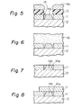
- polycrystalline silicon is deposited on the surfaces of insulating layer 11 and contact electrode 14b by a low-pressure chemical vapour deposition (C V D) method to form polycrystalline silicon layer 16.
- C V D chemical vapour deposition
- the thermal decomposition of silane (SiH 4 ) or the reduction of SiC14 (or SiH 2 C1 2 ) with hydrogen is carried out at a reaction temperature of from 600°C to 700°C so that it is impossible to use aluminum (Al) for contact electrode 14b.
- the wedge gap 15 can be completely filled with the polycrystalline silicon.
- Polycrystalline silicon layer 16 is etched to expose the surface of insulating layer 11 by a dry etching method, such as a reactive sputter etching method, as illustrated in Fig. 7. If the thickness of contact electrode 14b is equal to that of insulating layer 11, the surface of contact electrode 14b is also exposed. Wedge-shaped polycrystalline silicon portion 16a remains in the wedge gap so that a substantially level surface of the entire layer comprising insulating layer 11, contact electrode 14b, and wedge polycrystalline silicon portion 16a can be obtained.
- a dry etching method such as a reactive sputter etching method
- Al is deposited on the level surface (i.e., on the surface of insulating layer 11, wedge polycrystalline silicon portion 16a, and contact electrode 14b) by a vacuum evaporation method to form a conductor layer 17 without causing cracks to form.
- Conductor (Al) layer 17 is selectively etched by a conventional photoetching method to form a conductor line for interconnection. It is possible to use one of the above-mentioned high-melting point metals, such as Mo, Ta, Ti, W, or Pt, instead of Al. In this case, conductor layer 17 is formed by sputtering the high-melting point metal.
- the resultant device is heated so as to alloy wedge polycrystalline silicon portion 16a with the conductor line- and/or contact electrode 14b.
- the heating temperature is approximately 400°C to 500°C in the case of the Al conductor line and is from 900°C to 1000°C in the case of the high-melting point melt conductor line.
- Contact electrode 14b and the alloy of polycrystalline silicon portion 16a ensure an ohmic contact between conductor line and semiconductor substrate 12. Thus, a semiconductor device having a conductor line free of cracks can be produced.
- the alloying is carried out during the formation of PSG by the CVD method.
- a contact hole is formed in insulating layer 21 lying on semiconductor substrate 22 in the same manner as that of the first embodiment.
- the photoresist layer (not shown) on insulating layer 21 is removed with a suitable solvent.
- One of the above-mentioned high-melting point metals is deposited on insulating layer 21 and on the exposed portion of semiconductor substrate 22 by a sputtering method to form metal layer 23a and contact electrode 23b, respectively.
- Wedge gap 24 is formed between contact electrode 23b and the side of insulating layer 21.
- polycrystalline silicon is deposited on the surfaces of metal layer 23a and contact electrode 23b by a low-pressure CVD method to form polycrystalline silicon layer 25.
- the wedge gap is filled with polycrystalline silicon layer 25.
- polycrystalline silicon layer 25 and metal layer 23a are etched by a dry etching method so as to expose the surface of insulating layer 21.
- the obtained structure having a level surface is the same as that illustrated in Fig. 7.
- a conductor line of Al or of one of the above-mentioned high-melting point metals is formed and then a heat treatment for alloying of the portion of polycrystalline silicon layer 25 remaining in the wedge gap with the conductor line and/or contact electrode 23b is carried out in the same manner as that of the first embodiment.
- a heat treatment for alloying of the portion of polycrystalline silicon layer 25 remaining in the wedge gap with the conductor line and/or contact electrode 23b is carried out in the same manner as that of the first embodiment.
- a contact hole is formed in insulating layer 31 lying on semiconductor substrate 32 in the same manner as that of the first embodiment.
- the photoresist layer (not shown) on insulating layer 31 is removed with a suitable solvent.
- Thin polycrystalline silicon layer 33 is formed on the exposed surfaces of insulating layer 31 and semiconductor substrate 32 by a low-pressure CVD method.
- the polycrystalline silicon layer 33 is heavily doped as deposited or by means of thermal impurity diffusion or ion implantation after the deposition.
- one of the above--mentioned high-melting point metals is deposited on thin polycrystalline silicon layer 33 by a sputtering method so that metal layer 34a and contact electrode 34b are formed.
- Contact electrode 34b is positioned within a blind hole of thin silicon layer 33, and a wedge gap is formed between contact electrode 34b and the vertical surface of thin silicon layer 33.
- the thicknesses of insulating layer 31, thin polycrystalline silicon layer 33, and metal layer 34a are approximately 800 nm, approximately 100 nm, and from 400 to 700 nm, respectively.
- Polycrystalline silicon is deposited on the entire exposed surface by a low-pressure CVD method to form polycrystalline silicon layer 35, with which the wedge gap is filled.
- polycrystalline silicon layer 35, metal layer 34a, and thin polycrystalline silicon layer 33 are etched by a dry etching method so as to expose the surface of insulating layer 31. Portion 35a of silicon layer 35 remains in the wedge gap.
- a conductor line (not shown) consisting of a high--melting point metal is formed by using a sputtering method and a photoetching method and then a heat treatment for alloying the polycrystalline silicon of wedge portion 35a and remaining thin layer 33 with the high-melting point metal of the conductor line and contact electrode 34b is carried out in the same manner as that of the first embodiment.
- a conductor line is made of Al
- the heat-treatment conditions are, for example, a heating temperature of 1000°C and a heating time of ten minutes.
- the Al conductor line is subjected to a heat treatment (annealing) at approximately 400°C to 500°C.
Landscapes
- Internal Circuitry In Semiconductor Integrated Circuit Devices (AREA)
Applications Claiming Priority (2)
| Application Number | Priority Date | Filing Date | Title |
|---|---|---|---|
| JP56114716A JPS5815250A (ja) | 1981-07-21 | 1981-07-21 | 半導体装置の製造方法 |
| JP114716/81 | 1981-07-21 |
Publications (3)
| Publication Number | Publication Date |
|---|---|
| EP0070737A2 true EP0070737A2 (de) | 1983-01-26 |
| EP0070737A3 EP0070737A3 (en) | 1984-06-06 |
| EP0070737B1 EP0070737B1 (de) | 1986-10-01 |
Family
ID=14644827
Family Applications (1)
| Application Number | Title | Priority Date | Filing Date |
|---|---|---|---|
| EP82303828A Expired EP0070737B1 (de) | 1981-07-21 | 1982-07-21 | Halbleiteranordnung mit einer Elektrode und Verfahren zu deren Herstellung |
Country Status (4)
| Country | Link |
|---|---|
| US (1) | US4801559A (de) |
| EP (1) | EP0070737B1 (de) |
| JP (1) | JPS5815250A (de) |
| DE (1) | DE3273569D1 (de) |
Cited By (8)
| Publication number | Priority date | Publication date | Assignee | Title |
|---|---|---|---|---|
| FR2563048A1 (fr) * | 1984-04-13 | 1985-10-18 | Efcis | Procede de realisation de contacts d'aluminium a travers une couche isolante epaisse dans un circuit integre |
| FR2566181A1 (fr) * | 1984-06-14 | 1985-12-20 | Commissariat Energie Atomique | Procede d'autopositionnement d'une ligne d'interconnexion sur un trou de contact electrique d'un circuit integre |
| EP0123309A3 (en) * | 1983-04-25 | 1987-09-30 | Siemens Aktiengesellschaft Berlin Und Munchen | Method of producing stable, low ohmic contacts in integrated semiconductor circuits |
| EP0211888A4 (de) * | 1985-01-29 | 1988-08-04 | Ramtron Corp | Verfahren zur herstellung einer integrierten ferroelektrischen anordnung und so erzeugte anordnung. |
| EP0228183A3 (de) * | 1985-11-27 | 1989-10-18 | Kabushiki Kaisha Toshiba | Verfahren zur Herstellung eines Halbleiterbauelementes |
| EP0561132A1 (de) * | 1992-02-26 | 1993-09-22 | International Business Machines Corporation | Mit feuerfestem Metall aus PVD und CVD bedeckte Metalleiterbahnen und Durchgangsleitungen niedrigen Widerstandes |
| US6350676B1 (en) | 1991-11-22 | 2002-02-26 | Sgs-Thomson Microelectronics, S.R.L. | Method of forming high-stability metallic contacts in an integrated circuit with one or more metallized layers |
| WO2010005866A1 (en) * | 2008-07-11 | 2010-01-14 | Sandisk 3D Llc | Method of making a nonvolatile memory device |
Families Citing this family (17)
| Publication number | Priority date | Publication date | Assignee | Title |
|---|---|---|---|---|
| US4961822A (en) * | 1989-04-17 | 1990-10-09 | Liao Kuan Y | Fully recessed interconnection scheme with titanium-tungsten and selective CVD tungsten |
| JP2954263B2 (ja) * | 1990-03-22 | 1999-09-27 | 沖電気工業株式会社 | 半導体装置の製造方法 |
| US5540810A (en) * | 1992-12-11 | 1996-07-30 | Micron Technology Inc. | IC mechanical planarization process incorporating two slurry compositions for faster material removal times |
| US5950099A (en) * | 1996-04-09 | 1999-09-07 | Kabushiki Kaisha Toshiba | Method of forming an interconnect |
| JP2001118927A (ja) * | 1999-10-22 | 2001-04-27 | Mitsubishi Electric Corp | 半導体装置およびその製造方法 |
| US6774488B2 (en) * | 2001-10-22 | 2004-08-10 | Winbond Electronics Corp. | Low leakage and low resistance for memory and the manufacturing method for the plugs |
| CN1301551C (zh) * | 2002-12-13 | 2007-02-21 | 华邦电子股份有限公司 | 存储器制造方法及装置 |
| US7348672B2 (en) * | 2005-07-07 | 2008-03-25 | Taiwan Semiconductor Manufacturing Co., Ltd. | Interconnects with improved reliability |
| US20070052047A1 (en) * | 2005-09-01 | 2007-03-08 | Costas Hadjiloucas | Metal contact systems for semiconductor-based pressure sensors exposed to harsh chemical and thermal environments |
| US20100068235A1 (en) * | 2008-09-16 | 2010-03-18 | Searete LLC, a limited liability corporation of Deleware | Individualizable dosage form |
| US20100068153A1 (en) * | 2008-09-16 | 2010-03-18 | Searete Llc, A Limited Liability Corporation Of The State Of Delaware | Ex vivo activatable final dosage form |
| US20100068254A1 (en) * | 2008-09-16 | 2010-03-18 | Mahalaxmi Gita Bangera | Modifying a medicament availability state of a final dosage form |
| US20100069821A1 (en) * | 2008-09-16 | 2010-03-18 | Searete Llc, A Limited Liability Corporation Of The State Of Delaware | Ex vivo modifiable medicament release-sites final dosage form |
| US20100068152A1 (en) * | 2008-09-16 | 2010-03-18 | Searete Llc, A Limited Liability Corporation Of The State Of Delaware | Ex vivo modifiable particle or polymeric based final dosage form |
| US20100068275A1 (en) * | 2008-09-16 | 2010-03-18 | Searete Llc, A Limited Liability Corporation Of The State Of Delaware | Personalizable dosage form |
| US20100068233A1 (en) * | 2008-09-16 | 2010-03-18 | Searete Llc, A Limited Liability Corporation Of The State Of Delaware | Modifiable dosage form |
| US20100068256A1 (en) * | 2008-09-16 | 2010-03-18 | Searete Llc, A Limited Liability Corporation Of The State Of Delaware | Ex vivo modifiable medicament release-substance |
Family Cites Families (15)
| Publication number | Priority date | Publication date | Assignee | Title |
|---|---|---|---|---|
| DE1806980A1 (de) * | 1967-11-15 | 1969-06-19 | Fairchild Camera Instr Co | Halbleiter-Bauelement |
| US4017886A (en) * | 1972-10-18 | 1977-04-12 | Hitachi, Ltd. | Discrete semiconductor device having polymer resin as insulator and method for making the same |
| US3946476A (en) * | 1975-01-22 | 1976-03-30 | Dracon Industries | Automatic multi-conductor quick connect termination tool |
| JPS522166A (en) * | 1975-06-24 | 1977-01-08 | Hitachi Ltd | Method of pulling out wiring from highly inpure dope layer |
| JPS5228868A (en) * | 1975-08-29 | 1977-03-04 | Hitachi Ltd | Semiconductor device |
| US4045594A (en) * | 1975-12-31 | 1977-08-30 | Ibm Corporation | Planar insulation of conductive patterns by chemical vapor deposition and sputtering |
| JPS52106675A (en) * | 1976-03-05 | 1977-09-07 | Toshiba Corp | Manufacturing method of semiconductor device |
| JPS5317393A (en) * | 1976-07-31 | 1978-02-17 | Mitsubishi Heavy Ind Ltd | Commodities delivery detector |
| US4164461A (en) * | 1977-01-03 | 1979-08-14 | Raytheon Company | Semiconductor integrated circuit structures and manufacturing methods |
| JPS5917852B2 (ja) * | 1977-02-07 | 1984-04-24 | 日本電気株式会社 | 半導体装置 |
| US4109372A (en) * | 1977-05-02 | 1978-08-29 | International Business Machines Corporation | Method for making an insulated gate field effect transistor utilizing a silicon gate and silicide interconnection vias |
| JPS543480A (en) * | 1977-06-09 | 1979-01-11 | Fujitsu Ltd | Manufacture of semiconductor device |
| JPS5585042A (en) * | 1978-12-21 | 1980-06-26 | Mitsubishi Electric Corp | Semiconductor device |
| US4291322A (en) * | 1979-07-30 | 1981-09-22 | Bell Telephone Laboratories, Incorporated | Structure for shallow junction MOS circuits |
| JPS5932151A (ja) * | 1982-08-18 | 1984-02-21 | Nippon Telegr & Teleph Corp <Ntt> | 半導体装置の製造方法 |
-
1981
- 1981-07-21 JP JP56114716A patent/JPS5815250A/ja active Granted
-
1982
- 1982-07-21 EP EP82303828A patent/EP0070737B1/de not_active Expired
- 1982-07-21 DE DE8282303828T patent/DE3273569D1/de not_active Expired
-
1988
- 1988-02-29 US US07/165,367 patent/US4801559A/en not_active Expired - Fee Related
Cited By (16)
| Publication number | Priority date | Publication date | Assignee | Title |
|---|---|---|---|---|
| EP0123309A3 (en) * | 1983-04-25 | 1987-09-30 | Siemens Aktiengesellschaft Berlin Und Munchen | Method of producing stable, low ohmic contacts in integrated semiconductor circuits |
| EP0165085A1 (de) * | 1984-04-13 | 1985-12-18 | STMicroelectronics S.A. | Verfahren zur Herstellung von Aluminiumkontakten mit einer integrierten Schaltung durch eine dicke Isolierschicht hindurch |
| FR2563048A1 (fr) * | 1984-04-13 | 1985-10-18 | Efcis | Procede de realisation de contacts d'aluminium a travers une couche isolante epaisse dans un circuit integre |
| FR2566181A1 (fr) * | 1984-06-14 | 1985-12-20 | Commissariat Energie Atomique | Procede d'autopositionnement d'une ligne d'interconnexion sur un trou de contact electrique d'un circuit integre |
| EP0170544A1 (de) * | 1984-06-14 | 1986-02-05 | Commissariat A L'energie Atomique | Verfahren zur Selbstjustierung eines Verbindungsleiters über einem elektrischen Kontaktloch einer integrierten Schaltung |
| US4624864A (en) * | 1984-06-14 | 1986-11-25 | Commissariat A L'energie Atomique | Process for the autopositioning of an interconnection line on an electric contact hole of an integrated circuit |
| EP0211888A4 (de) * | 1985-01-29 | 1988-08-04 | Ramtron Corp | Verfahren zur herstellung einer integrierten ferroelektrischen anordnung und so erzeugte anordnung. |
| EP0228183A3 (de) * | 1985-11-27 | 1989-10-18 | Kabushiki Kaisha Toshiba | Verfahren zur Herstellung eines Halbleiterbauelementes |
| US6350676B1 (en) | 1991-11-22 | 2002-02-26 | Sgs-Thomson Microelectronics, S.R.L. | Method of forming high-stability metallic contacts in an integrated circuit with one or more metallized layers |
| EP0561132A1 (de) * | 1992-02-26 | 1993-09-22 | International Business Machines Corporation | Mit feuerfestem Metall aus PVD und CVD bedeckte Metalleiterbahnen und Durchgangsleitungen niedrigen Widerstandes |
| US5889328A (en) * | 1992-02-26 | 1999-03-30 | International Business Machines Corporation | Refractory metal capped low resistivity metal conductor lines and vias |
| US5976975A (en) * | 1992-02-26 | 1999-11-02 | International Business Machines Corporation | Refractory metal capped low resistivity metal conductor lines and vias |
| US6147402A (en) * | 1992-02-26 | 2000-11-14 | International Business Machines Corporation | Refractory metal capped low resistivity metal conductor lines and vias |
| US6323554B1 (en) | 1992-02-26 | 2001-11-27 | International Business Machines Corporation | Refractory metal capped low resistivity metal conductor lines and vias formed using PVD and CVD |
| EP0788156A3 (de) * | 1992-02-26 | 1998-04-15 | International Business Machines Corporation | Mit feuerfestem Metall aus PVD und CVD bedeckte Metallleiterbahnen und Durchgangsleitungen niedrigen Widerstandes |
| WO2010005866A1 (en) * | 2008-07-11 | 2010-01-14 | Sandisk 3D Llc | Method of making a nonvolatile memory device |
Also Published As
| Publication number | Publication date |
|---|---|
| US4801559A (en) | 1989-01-31 |
| JPS637464B2 (de) | 1988-02-17 |
| EP0070737B1 (de) | 1986-10-01 |
| EP0070737A3 (en) | 1984-06-06 |
| JPS5815250A (ja) | 1983-01-28 |
| DE3273569D1 (en) | 1986-11-06 |
Similar Documents
| Publication | Publication Date | Title |
|---|---|---|
| EP0070737B1 (de) | Halbleiteranordnung mit einer Elektrode und Verfahren zu deren Herstellung | |
| KR910002455B1 (ko) | 반도체장치 제조방법 | |
| EP0499433B1 (de) | Halbleiter-Vorrichtung mit Verdrahtung der verbesserten Zuverlässigkeit und Verfahren zu ihner Herstellung | |
| KR0179822B1 (ko) | 반도체 장치의 배선 구조 및 그 제조 방법 | |
| US5183782A (en) | Process for fabricating a semiconductor device including a tungsten silicide adhesive layer | |
| US4708904A (en) | Semiconductor device and a method of manufacturing the same | |
| JPH1098100A (ja) | コンタクトホール/スルーホール形成方法 | |
| US4589196A (en) | Contacts for VLSI devices using direct-reacted silicide | |
| US5414404A (en) | Semiconductor device having a thin-film resistor | |
| US3856648A (en) | Method of forming contact and interconnect geometries for semiconductor devices and integrated circuits | |
| JPS63133648A (ja) | タングステン被覆法 | |
| EP0147247A2 (de) | Verfahren zum Herstellen einer Protuberanz-Unterdrückungsschicht in der Doppelmetallschicht-Verarbeitung und so hergestellte Struktur | |
| JP2798250B2 (ja) | アルミニウム物質との低抵抗接点形成方法,およびアルミニウムとの低抵抗接点 | |
| JPH11111842A (ja) | 多層配線構造およびその製造方法 | |
| US4890151A (en) | Thin-film and its forming method | |
| KR0139599B1 (ko) | 반도체 장치의 금속배선 형성방법 | |
| KR100191710B1 (ko) | 반도체 소자의 금속 배선 방법 | |
| US5663094A (en) | Process for producing semiconductor device with wire for three conductive layers | |
| JPS5961147A (ja) | 半導体装置の製造方法 | |
| KR100373364B1 (ko) | 금속배선 형성방법 | |
| KR100186985B1 (ko) | 반도체 소자의 콘택홀 매립 금속배선 형성방법 | |
| KR100369352B1 (ko) | 반도체 장치 및 그 제조방법 | |
| KR930002662B1 (ko) | 반도체 제조에서 미세 금속 배선의 형성 방법 | |
| JPS59163822A (ja) | 半導体装置の製造方法 | |
| JPH0677162A (ja) | 半導体装置とその製法 |
Legal Events
| Date | Code | Title | Description |
|---|---|---|---|
| PUAI | Public reference made under article 153(3) epc to a published international application that has entered the european phase |
Free format text: ORIGINAL CODE: 0009012 |
|
| AK | Designated contracting states |
Designated state(s): DE FR GB |
|
| PUAL | Search report despatched |
Free format text: ORIGINAL CODE: 0009013 |
|
| AK | Designated contracting states |
Designated state(s): DE FR GB |
|
| 17P | Request for examination filed |
Effective date: 19840822 |
|
| GRAA | (expected) grant |
Free format text: ORIGINAL CODE: 0009210 |
|
| AK | Designated contracting states |
Kind code of ref document: B1 Designated state(s): DE FR GB |
|
| REF | Corresponds to: |
Ref document number: 3273569 Country of ref document: DE Date of ref document: 19861106 |
|
| ET | Fr: translation filed | ||
| PLBE | No opposition filed within time limit |
Free format text: ORIGINAL CODE: 0009261 |
|
| STAA | Information on the status of an ep patent application or granted ep patent |
Free format text: STATUS: NO OPPOSITION FILED WITHIN TIME LIMIT |
|
| 26N | No opposition filed | ||
| PGFP | Annual fee paid to national office [announced via postgrant information from national office to epo] |
Ref country code: GB Payment date: 19920713 Year of fee payment: 11 |
|
| PGFP | Annual fee paid to national office [announced via postgrant information from national office to epo] |
Ref country code: FR Payment date: 19920730 Year of fee payment: 11 |
|
| PGFP | Annual fee paid to national office [announced via postgrant information from national office to epo] |
Ref country code: DE Payment date: 19920922 Year of fee payment: 11 |
|
| PG25 | Lapsed in a contracting state [announced via postgrant information from national office to epo] |
Ref country code: GB Effective date: 19930721 |
|
| GBPC | Gb: european patent ceased through non-payment of renewal fee |
Effective date: 19930721 |
|
| PG25 | Lapsed in a contracting state [announced via postgrant information from national office to epo] |
Ref country code: FR Effective date: 19940331 |
|
| PG25 | Lapsed in a contracting state [announced via postgrant information from national office to epo] |
Ref country code: DE Effective date: 19940401 |
|
| REG | Reference to a national code |
Ref country code: FR Ref legal event code: ST |