EP0074642A2 - Schnelle, verlustarme Dioden - Google Patents
Schnelle, verlustarme Dioden Download PDFInfo
- Publication number
- EP0074642A2 EP0074642A2 EP82108373A EP82108373A EP0074642A2 EP 0074642 A2 EP0074642 A2 EP 0074642A2 EP 82108373 A EP82108373 A EP 82108373A EP 82108373 A EP82108373 A EP 82108373A EP 0074642 A2 EP0074642 A2 EP 0074642A2
- Authority
- EP
- European Patent Office
- Prior art keywords
- diode
- epitaxial layer
- type epitaxial
- layer
- schottky
- Prior art date
- Legal status (The legal status is an assumption and is not a legal conclusion. Google has not performed a legal analysis and makes no representation as to the accuracy of the status listed.)
- Granted
Links
Images



Classifications
-
- H—ELECTRICITY
- H10—SEMICONDUCTOR DEVICES; ELECTRIC SOLID-STATE DEVICES NOT OTHERWISE PROVIDED FOR
- H10D—INORGANIC ELECTRIC SEMICONDUCTOR DEVICES
- H10D64/00—Electrodes of devices having potential barriers
- H10D64/60—Electrodes characterised by their materials
- H10D64/64—Electrodes comprising a Schottky barrier to a semiconductor
-
- H—ELECTRICITY
- H10—SEMICONDUCTOR DEVICES; ELECTRIC SOLID-STATE DEVICES NOT OTHERWISE PROVIDED FOR
- H10D—INORGANIC ELECTRIC SEMICONDUCTOR DEVICES
- H10D64/00—Electrodes of devices having potential barriers
- H10D64/01—Manufacture or treatment
- H10D64/012—Manufacture or treatment of electrodes comprising a Schottky barrier to a semiconductor
- H10D64/0121—Manufacture or treatment of electrodes comprising a Schottky barrier to a semiconductor to Group IV semiconductors
-
- H—ELECTRICITY
- H10—SEMICONDUCTOR DEVICES; ELECTRIC SOLID-STATE DEVICES NOT OTHERWISE PROVIDED FOR
- H10D—INORGANIC ELECTRIC SEMICONDUCTOR DEVICES
- H10D8/00—Diodes
- H10D8/60—Schottky-barrier diodes
Definitions
- This invention relates to rectifying diodes suited for high speed power switching purposes.
- the electric properties required for rectifying diodes for switching power sources are:
- Diodes are based on the most basic principles and structure among semiconductor elements, and unlike ICs it is difficult to vary their characteristics over wide ranges with corresponding variety of circuit constructions and patterns. Therefore, the gist of the .improvement of power diodes is how to modify the basic operational principles and structure for obtaining the electric properties listed above to the utmost.
- the diodes which are practically used for high speed power rectification are of two types, i.e., Schottky diode and pn junction diode. Each type has disadvantages as described below and its range of application is limited.
- the Schottky diode is presently most excellent since it is-a majority carrier element having fast reverse recovering speeds.
- the Schottky diode has further advantages of lower forward voltage than that of the pn junction diode and capability of high efficiency operation.
- Schottky diodes conventionally used have a breakdown voltage which is about 50 V at the most, so that its use has essentially been limited only to low voltage applications.
- the Schottky diode has a large junction capacitance and hence its upper limit of permissible temperature is low.
- the Schottky diode of a general structure comprises a low resistivity n-type substrate, an n-type epitaxial layer deposited on the substrate and a metal electrode or Schottky electrode forming a Schottky junction with the n-type epitaxial layer.
- the resistivity of the silicon n-type substrate is usually set to be 0.1 n cm or less preferably 0.02 ⁇ cm or less.
- both the resistivity and thickness of the n-type epitaxial layer may be selected to high values. Doing so, however, increases the resistance of the n-type epitaxial layer to greatly increase the parasitic voltage drop that develops across the n-type epitaxial layer when a forward current is passed. Therefore, there are restrictions on these parameters, and it has been common in the conventional power Schottky to set the resistivity and thickness of the silicon n-type epitaxial layer to 1 ⁇ cm or less and 3 ⁇ m or less, respectively. For these reasons, the practical breakdown voltage has been within approximately 50 V as has been mentioned. In this respect, one may refer to "Theoretical Performance of the Schottky Barrier Power Rectifier" by D. J. Page, SSE Vol. 15, No. 5-C, page 509, and "Comparison of the pn Fast Switching Rectifier and the Schottky Rectifier” by Robert A Smith et al, IAS 76 Annual, page 61.
- the inevitable reduction in thickness and resistivity of the n-type epitaxial layer in the conventional Schottky diode is due to the fact that because the Schottky diode is a majority carrier element and the conductivity modulation of the n-type epitaxial layer by means of minority carriers (hole) cannot be expected, the resistivity of the n-type epitaxial layer acting by itself as a diode series resistor must be reduced to decrease the forward voltage. As a result, breakdown voltage is decreased and junction capacitance is increased.
- pn junction diodes are often used because high voltages are involved.
- the pn junction diode has a small reverse recovery speed (about 0.5 ⁇ s or more in terms of recovery time) due to the storage of minority carriers and is unsuitable for high speed operation.
- a typical structure of the conventional pn junction diode comprises a low resistivity n-type substrate, a high resistivity p-type expitaxial layer deposted on the substrate and a p contact layer of high impurity concentration formed in the epitaxial layer. Further, metal electrodes are formed on surfaces of the n-type substrate and p contact layer, respectively. The p contact layer and the metal electrode thereon forms a so-called low-high electrode.
- the resistivity of the n-type substrate and p contact layer is usually set to 0.1 ⁇ cm or less, preferably 0.02 ⁇ cm or less.
- the resistivity of the p-type epitaxial layer is set to 1 ⁇ cm or more in order to ensure sufficient breakdown voltage. In this case, the impurity concentration in the p contact layer is set to 5 x 10 18 cm -3 or more.
- a gold doped diode For attainment of high speed operation, a gold doped diode has been manufactured wherein an epitaxial layer of a pn junction diode is doped with gold.
- the upper limit of the permissible temperature is reduced, that is, one of the features of the pn junction diode is lost.
- the forward voltage is increased and the uniformity of manufacture is reduced. Switching noise is also increased.
- the present invention contemplates elimination of the aforementioned disadvantages of the conventional S chottky and pn junction diodes and has for its object to provide a diode of low loss, high speed, high breakdown voltage, high temperature resistance and low noise.
- the above object is accomplished by a diode having a Schottky barrier which permits bidirectional passage of minority carriers as well as majority carriers as an electrode that substitutes for the conventional Schottky electrode in Schottky diodes and low-high electrode in pn junction diodes.
- structural parameters of the diode according to the invention are set to fall within a range which is considerably different from that of the conventional diodes.
- the diode of the invention takes the form of a pn junction diode having a Schottky barrier electrode, providing a novel structure of pn junction diode.
- the diode has a Schottky barrier contact which permits bidirectional passage of minority carriers as well as majority carriers as an electrode
- the upper and lower limits are specified as:
- the range of ⁇ h is preferably, for the Schottky diode.
- the speed is approximately the same as or higher than the speed of the conventional Schottky diode, and nevertheless the breakdown voltage is higher, the junction capacitance is lower, and the upper limit of the permissible temperature is higher.
- the pn junction diode of the invention stability and robustness are substantially the same as with the conventional pn junction diode without gold doping, and nevertheless the permissible temperature is higher, the breakdown voltage is higher, the speed is higher and the forward voltage is lower. In comparison to the gold-doped high speed diode, the permissible temperature is higher, the switching noise is less, and the forward voltage is lower.
- the invention will first be described by way of example in the form of a Schottky diode.
- the inventors of the present invention have conducted extensive analysis and experiments and found that under certain conditions conductivity modulation of the n-type epitaxial layer can be produced during forward current conduction in Schottky diodes without sacrifice of the reverse recovery characteristic at all.
- the invention is predicated on this finding to provide the following ranges of structural parameters of the Schottky diode. Specifically, with reference to Fig.
- FIG. 1 showing a schematic construction of a Schottky diode according to the invention in a predetermined range of the thickness of an n-type epitaxial layer 2 deposited on an n-type substrate 1, the potential barrier value ⁇ B of the Schottky junction with respect to electrons (majority carriers represented by ⁇ in the figure) and the potential barrier value ⁇ h of the junction with respect to holes (minority carriers represented by ⁇ in the figure) as shown in Fig. 2 are set to fall within ranges within which a sufficient quantity of holes to effect conductivity modulation of the n-type epitaxial layer 2 can flow from a metal electrode 3 into the n-type epitaxial layer 2 in a forwardly biased state of the Schottky diode.
- FIG. 2 shows an energy level diagram of the Schottky diode shown in Fig. 1.
- regions (a), (b) and (c) correspond to the n-type substrate 1, n-type epitaxial layer 2 and metal electrodes 3 (Schottky electrode), respectively. Shown at F is the Fermi level.
- the resistivity P and thickness W1 of the n-type epitaxial layer 2 that are required for materializing an actual high breakdown voltage Schottky diode will be discussed.
- the metal electrode 3 in the structure of Fig. 1 is made negative with respect to the n-type substrate 1
- a depletion layer is developed to extend from the boundary between the n-type epitaxial layer 2 and metal electrode 3, i.e., the Schottky junction, into the n-type epitaxial layer 2.
- the resistivity p of the n-type epitaxial layer 2 is increased, the breakdown voltage is also increased.
- the depletion layer cannot extend beyond the thickness of the n-type epitaxial layer 2, so that the breakdown voltage cannot be increased beyond a certain value with increasing resistivity ⁇ .
- the maximum breakdown voltage is equal to the product of the avalanche electric field value of the semiconductor and the thickness of the n-type epitaxial layer 2.
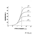
- Fig. 3 shows the relation between the breakdown voltage and the resistivity p of the n-type epitaxial layer 2 in the case of silicon Schottky diodes for different values of the thickness of the n-type epitaxial layer 2 ranging from 5 to 20pm.
- Curves (a), (b), (c) and (d) correspond to cases where the thickness of the n-type epitaxial layer 2 is respectively 5 ⁇ m, 10 ⁇ m, 15 ⁇ m and 20 ⁇ m.
- the thickness value of 5 ⁇ m is a minimum value necessaryy for obtaining a breakdown voltage which is definitely higher than (at least double) the breakdown voltage (50 V) of the prior art Schottky diode.
- Thickness value of 20 Um is a maximum value in view of avoiding the deterioration of the operation speed characteristics of the Schottky diode under the injection of holes characteristic to the S chottky diode of this invention as will be described later.
- the resistivity p of the n-type epitaxial layer 2 is desirably at least 10 Qcm, preferably above, for effectively realizing the high breakdown voltage characteristic. It will be appreciated that the n-type epitaxial layer 2 may be of a multi-layer.
- a current versus voltage characteristic different from that in the prior art can be obtained as shown in Fig. 4.
- a tendency similar to the characteristic of the usual Schottky diode can be obtained within a comparatively low applied voltage range as indicated at A.
- scales are in logarithm for both the ordinate and abscissa.
- the characteristic is curved as shown at B due to the series resistance of the n-type epitaxial layer 2 in the case of the prior art Schottky diode. If this tendency would continue, the forward voltage would sharply increase /by the
- the potential barrier value 6h of the Schottky junction with respect to holes is set to be below a certain value.
- conductivity modulation by holes injected from the metal electrode 3 into the n-type epitaxial layer 2 can be obtained to reduce the series resistance effect of the high resistivity n-type epitaxial layer 2.
- the forward voltage can be reduced for the normal current range as shown at D in Fig. 4.
- the conductivity modulation becomes insufficient because there is an upper limit of the quantity of holes injected by jumping over the potential barrier of ph. Therefore, the forward voltage is sharply increased as shown at E. It will be seen that the upper limit of ⁇ h must be set such that this sharply increasing region is outside the normal current range.
- the potential barrier value ⁇ h of the Schottky junction with respect to holes also has a lower limit. If the value of ⁇ h is over-decreased, excessive hole injection and large hole accumulation happen, which decreases the operation speed of the element.
- ⁇ h The upper and lower limits of ⁇ h are determined in the case of silicon Schottky diodes as follows.
- the sum of ⁇ B and ⁇ h is always equal to the fobidden band width of 1.1 eV unless a special structure as will be described later is adopted. For this reason, in the abscissa the values ⁇ B and ⁇ h are graduated in opposite directions.
- solid curves represent the forward voltage
- chained line curves represent the hole storage time.
- the curves (a), (b) and (c) correspond to cases where the thickness of the n-type epitaxial layer 2 is respectively 5 ⁇ m, 15 ⁇ m and 20 ⁇ m.
- the forward voltage is plotted at 300 A/cm 2
- the hole storage time is plotted at a maximum value within the current density range.
- the sharp increase of the forward voltage in the right hand part of the graph of Fig. 5 is due to insufficient conductivity modulation that results from the reduction in quantity of holes injected into the n-type epitaxial layer 2 with increasing ⁇ h.
- the sharp increase of the hole storage time in the left hand part of the graph is attributable to a sharp upward curving of the conduction band of the n-type epitaxial layer 2 in the neighborhood of the Schottky junction with decreasing ⁇ h. It will be seen from the graph that for the structure according to the invention, it is necessary to set ⁇ h to be 0.1 eV ⁇ h ⁇ 0.4 eV, as shown by thick arrows in the graph.
- the range of ⁇ h is preferably, 0.15 eV ⁇ h ⁇ 0.35 eV as shown by thin arrows. It will also be seen that the thickness of the n-type epitaxial layer 2 must be 20 ⁇ m or less in order to ensure a high speed comparable to that of the prior art Schottky diode (approximately 40 ns ).
- a guard ring 7 is then formed from the surface of the layer 2 to a depth of 1 ⁇ m with a surface impurity concentration of 5 x 10 18 cm -3 . Then, an edge portion of the guard ring is etched to a depth of 5 ⁇ m to form a mesa.
- an oxide film 4 with a thickness of approximately 0.6 ⁇ m is formed by oxidation for protection of the guard ring edge.
- a Schottky electrode 3 is formed by depositing platinum to a thickness of 0.5 um.
- a metal electrode 8 is formed on the back side by doping an n-type impurity at a surface impurity concentration of 1 x 10 20 cm -3 or more and then depositing nickel to a thickness of 0.2 ⁇ m and then silver to a thickness of 0.5 ⁇ m. After the electrode formation, heat treatment is carried out at 450°C for 20 minutes. The diode thus obtained has an effective area of 20 mm 2.
- Fig. 7 shows reverse current versus reverse voltage characteristics of the diode thus obtained in comparison with those of the conventional Schottky diode.
- temperatures are permissible temperatures.
- a breakdown voltage of 200 V or more can be obtained, and permissible temperature of the junction may be about 200°C.
- the breakdown voltage is restricted by the yield voltage of the mesa portion of the p-type guard ring, and further improvement of the breakdown voltage is possbile.
- Fig. 8 shows a reverse recovery characteristic of the Schottky diode. This curve represents current plotted against time, and is obtained by first causing a forward current of 30 A and then reducing it at a rate of 50 A/ ⁇ s.
- This diode thus has a high speed comparable to that of the prior art Schottky diode (i.e., 30 to 50 ns ).
- the forward voltage of this diode is 0.75 V when the current passed is 30 A.
- Fig. 9 shows a modified structure of a silicon Schottky diode according to the invention where a metal electrode 3 is formed using a metal which fails to meet the condition ⁇ B ⁇ 1.0 eV although it meets the condition ⁇ h ⁇ 0.4 eV.
- This structure is different from the structure shown in Fig. 1 in that a thin n-type intervening layer 5 of a high impurity concentration is provided at the boundary between the n-type epitaxial layer 2 and metal electrode (i.e., Schottky electrode) 3.
- the thickness of the n-type intervening layer 5 must be smaller than the thickness or depth of the depletion layer that is developed from the Schottky electrode 3 in the zero bias state, for instance 100 A or less when the impurity concentration is 10 18 to 1020 cm -3 .
- a high electric field intensity zone is formed in the depletion layer in the neighborhood of a region (c) corresponding to the Schottky electrode 3 as shown in Fig. 10. Electrons can freely pass through this zone due to the tunnel effect, so that the effective potential barrier value ⁇ B' with respect to electrons becomes smaller than the actual potential barrier value pB. That is, the condition ⁇ B (i.e., ⁇ B') ⁇ 1.0 eV can be met equivalently.
- a region (d) corresponds to the n-type intervening layer 5. The effective reduction of ⁇ B by this method can be satisfactorily controllable if ⁇ B is 0.1 to 0.2 eV.
- ⁇ B is desirably as high as possible in the aforementioned range from the standpoint of the reduction of the leakage current. It is possible to increase ⁇ B equivalently in the following way.
- a thin p-type intervening layer 6 is provided between n-type epitaxial layer 2 and Schottky electrode 3.
- the effective potential barrier value ⁇ B' of the Schottky junction with respect to electrons can be made greater than the actual value pB as shown in Fig. 12.
- a region (e) corresponds to the p-type intervening layer 6.
- the effective value ⁇ B' is of course to be suppressed to 1.0 eV or less.
- the electric field intensity in the neighborhood of the Schottky junction can be reduced to reduce ⁇ B by virtue of a region (f) corresponding to the intervening layer as shown in Fig. 13.
- the invention is applicable to a pn junction diode as will be described with reference to Fig. 14 showing a schematic construction of this embodiment.
- the pn junction diode of this embodiment has a high resistivity p-type epitaxial layer 12 which makes direct contact to a metal electrode 15 to form a Schottky junction.
- Denoted by 14 is a metal electrode.
- Fig. 15 shows an energy level diagram of this structure.
- the conduction band in a region (b) which corresponds to the high resistivity p-type epitaxial layer 12 is downwardly curved in the neighborhood of the contact of this region with a region (d) which corresponds to the metal electrode 15.
- electrons (minority carriers) coming from a region (a) which corresponds to the n-type substrate 11 flow into the metal electrode 15 without being excessively stored in the p-type epitaxial layer 12.
- the potential barrier ⁇ h is excessive, insufficient holes are supplied so that the forward voltage is extremely increased. In this case, the element can no longer be normally used. If the potential barrier ⁇ B is excessive, the conduction band in the p-type epitaxial layer 12 is greatly curved upwards at the Schottky junction. In this case, like the high impurity concentration p contact structure shown in Fig. 16, the reverse recovery speed of the diode is reduced with increased charge storage effect.
- the potential barrier values ⁇ B and ⁇ h of the Schottky junction with respect to electrons and holes must be set in optimum ranges so that no barrier may be formed against the flow into the metal electrode 15 of electrons injected from the n-type substrate 11 to the p-type epitaxial layer 12 while permitting injection of holes from the metal electrode 15 into the p-type epitaxial layer 12.
- regions (a) and (b) correspond to the n-type substrate and the p-type epitaxial layer, respectively, and a region (c) corresponds to the high impurity concentration p contact region, that is, the aforementioned low-high electrode region.
- a minimum quantity of electrons necessary to cause forward current in a forwardly biased state must be present in the p-type epitaxial layer 12. In this case, however, if the thickness of the p-type epitaxial layer 12 is excessive, the quantity of electrons present in the layer is increased to reduce the reverse recovery speed. The thickness of the p-type epitaxial layer 12 is thus limited in this respect.
- thickness W 2 and resisitivity p of the p-type epitaxial layer 12 be determined such that a depletion layer that extends from the n-type substrate 11 to the p-type epitaxial layer 12 in a reversely biased state will not be in contact with the metal electrode (i.e., Schottky electrode) 15 forming the Schottky junction.
- the reverse leakage current is as small as in the usual pn junction diode without gold doping so that it can be ignored even at high temperatures.
- the obtainable breakdown voltage is up to approximately one half the product of the thickness of the p-type epitaxial layer and the avalanche electric field value of the semiconductor.
- curves (a), (b) and (c) are obtained in cases where the thickness of the p-type epitaxial layer 12 is respectively 5 ⁇ m, 15 ⁇ m, 20 pm and 30 ⁇ m.
- the thickness of 5 pm is the lower limit necessary for obtaining a breakdown voltage that can feature the structure of the pn junction diode according to this embodiment.
- the thickness of 30 ⁇ m is the upper limit from the standpoint of the reverse recovery speed as will be described later. Since the normal current density in a power diode is usually 50 to 300 A/cm 2 , the forward voltage is at 300 A/cm 2 , and the hole storage time is shown at a maximum value within the aforementioned current density range.
- the values in the graph are substantially independent of the resistivity p (>1 ⁇ cm) of the p-type epitaxial layer 12.
- An edge portion of the surface of the p-type epitaxial layer 12 is then etched to a depth of 30 ⁇ m to form a mesa portion. Then, an oxide film 16 is formed by oxidation for protecting the edge of the mesa portion.
- a metal electrode 14 is formed on the back side by doping an n-type impurity with a surface impurity concentration of 1 x 10 20 cm -3 or more and to a depth of approximately 1 ⁇ m and then depositing nickel to a thickness of 0.2 ⁇ m and then silver to a thickness of 0.5 ⁇ m.
- the pn junction diode thus formed has an effective area of 20 mm2 and a breakdown voltage of 220 V.
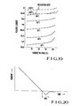
- Fig. 19 shows reverse characteristics of the pn junction diode according to this embodiment in comparison with those of the conventional high speed gold doped pn junction diode.
- temperatures are permissible temperatures.
- Table 2 For comparison of characteristics of the gold doped pn junction diode with those of the present diode, reference is made to Table 2 below.
- a diode body and heat sink fingers are put together to complete a power diode assembly.
- the diode, according to both the former and latter embodiments, having the high upper limit of permissible temperature can effectively reduce the area of the heat sink fingers, thereby making it possible to reduce the size of the completed assembly.
- the surface area of heat sink fingers for the conventional Schottky diode is taken to be 1 (one)
- the finger surface area for the pn junction diode according to the invention can be reduced to about 45%.
- the Schottky diode of the invention the finger surface area can be reduced to about 75%.
- Fig. 20 shows the reverse recovery characteristic of the diode described above.
- the curve shows the current plotted against time, and is obtained by first causing a forward current of 30 A and then reducing it at a rate of 50 A/ps.
- the reverse recovery time is approximately 80 ns. With the usual pn junction diode, the reverse recovery time is from 200 nsec to 1 ⁇ sec. Thus, according to the present embodiment, the speed can be increased. It is to be noted from the Figure that reverse current has a trailing portion in the latter half of the reverse recovery to provide a soft recovery characteristic, resulting in a low switching noise and a low surge voltage. The forward voltage is 0.80 V when the current is 30 A.
- the pn junction diode embodying the invention has the Schottky electrode formed on the surface of the p-type epitaxial layer
- the invention is also applicable to a pn junction diode wherein an n-type epitaxial layer is deposited on a p-type substrate and a Schottky electrode is formed on the n-type epitaxial layer.
- an electrode which establishes the Schottky barrier that permits bidirectional passage of minority and majority carriers, and thickness and resistivity of the epitaxial layer adjoining the electrode are set to fall within the specified ranges, thereby improving electric properties required for rectifying diodes for the switching power source.
Landscapes
- Electrodes Of Semiconductors (AREA)
Applications Claiming Priority (8)
| Application Number | Priority Date | Filing Date | Title |
|---|---|---|---|
| JP56143640A JPS6031113B2 (ja) | 1981-09-11 | 1981-09-11 | 半導体装置 |
| JP143640/81 | 1981-09-11 | ||
| JP57004301A JPS58122782A (ja) | 1982-01-14 | 1982-01-14 | ダイオ−ド |
| JP4301/82 | 1982-01-14 | ||
| JP57031323A JPS58148469A (ja) | 1982-02-27 | 1982-02-27 | シヨツトキダイオ−ド |
| JP31323/83 | 1982-02-27 | ||
| JP57031322A JPS58148468A (ja) | 1982-02-27 | 1982-02-27 | 半導体装置 |
| JP31322/82 | 1982-02-27 |
Publications (3)
| Publication Number | Publication Date |
|---|---|
| EP0074642A2 true EP0074642A2 (de) | 1983-03-23 |
| EP0074642A3 EP0074642A3 (en) | 1984-12-27 |
| EP0074642B1 EP0074642B1 (de) | 1989-06-21 |
Family
ID=27454058
Family Applications (1)
| Application Number | Title | Priority Date | Filing Date |
|---|---|---|---|
| EP82108373A Expired EP0074642B1 (de) | 1981-09-11 | 1982-09-10 | Schnelle, verlustarme Dioden |
Country Status (4)
| Country | Link |
|---|---|
| US (1) | US4720734A (de) |
| EP (1) | EP0074642B1 (de) |
| CA (1) | CA1189634A (de) |
| DE (1) | DE3279779D1 (de) |
Cited By (1)
| Publication number | Priority date | Publication date | Assignee | Title |
|---|---|---|---|---|
| US5155565A (en) * | 1988-02-05 | 1992-10-13 | Minnesota Mining And Manufacturing Company | Method for manufacturing an amorphous silicon thin film solar cell and Schottky diode on a common substrate |
Families Citing this family (21)
| Publication number | Priority date | Publication date | Assignee | Title |
|---|---|---|---|---|
| US4952992A (en) * | 1987-08-18 | 1990-08-28 | Siliconix Incorporated | Method and apparatus for improving the on-voltage characteristics of a semiconductor device |
| JP3230829B2 (ja) * | 1992-01-14 | 2001-11-19 | 株式会社日立製作所 | 車両用交流発電機と整流器 |
| US5150176A (en) * | 1992-02-13 | 1992-09-22 | Motorola, Inc. | PN junction surge suppressor structure with moat |
| US5241195A (en) * | 1992-08-13 | 1993-08-31 | North Carolina State University At Raleigh | Merged P-I-N/Schottky power rectifier having extended P-I-N junction |
| JPH0964381A (ja) * | 1995-08-25 | 1997-03-07 | Murata Mfg Co Ltd | ショットキーバリアダイオード |
| WO1997027629A1 (en) * | 1996-01-24 | 1997-07-31 | Cree Research, Inc. | Mesa schottky diode with guard ring |
| DE19853743C2 (de) * | 1998-11-21 | 2000-10-12 | Micronas Intermetall Gmbh | Halbleiter-Bauelement mit wenigstens einer Zenerdiode und wenigstens einer dazu parallel geschalteten Schottky-Diode sowie Verfahren zum Herstellen der Halbleiter-Bauelemente |
| US6573128B1 (en) | 2000-11-28 | 2003-06-03 | Cree, Inc. | Epitaxial edge termination for silicon carbide Schottky devices and methods of fabricating silicon carbide devices incorporating same |
| US9515135B2 (en) * | 2003-01-15 | 2016-12-06 | Cree, Inc. | Edge termination structures for silicon carbide devices |
| US7026650B2 (en) | 2003-01-15 | 2006-04-11 | Cree, Inc. | Multiple floating guard ring edge termination for silicon carbide devices |
| US20050121691A1 (en) * | 2003-12-05 | 2005-06-09 | Jean-Luc Morand | Active semiconductor component with a reduced surface area |
| WO2005119793A2 (en) * | 2004-05-28 | 2005-12-15 | Caracal, Inc. | Silicon carbide schottky diodes and fabrication method |
| US7820473B2 (en) * | 2005-03-21 | 2010-10-26 | Semiconductor Components Industries, Llc | Schottky diode and method of manufacture |
| US7279390B2 (en) * | 2005-03-21 | 2007-10-09 | Semiconductor Components Industries, L.L.C. | Schottky diode and method of manufacture |
| US8901699B2 (en) | 2005-05-11 | 2014-12-02 | Cree, Inc. | Silicon carbide junction barrier Schottky diodes with suppressed minority carrier injection |
| US20070077738A1 (en) * | 2005-10-03 | 2007-04-05 | Aram Tanielian | Fabrication of small scale matched bi-polar TVS devices having reduced parasitic losses |
| US7821095B2 (en) * | 2006-07-14 | 2010-10-26 | Semiconductor Components Industries, Llc | Method of forming a Schottky diode and structure therefor |
| JP5755867B2 (ja) * | 2010-11-11 | 2015-07-29 | 日本インター株式会社 | 半導体装置 |
| WO2014008415A1 (en) * | 2012-07-05 | 2014-01-09 | Littelfuse, Inc. | Crowbar device for voltage transient circuit protection |
| WO2019097662A1 (ja) * | 2017-11-17 | 2019-05-23 | 新電元工業株式会社 | 電力変換回路 |
| DE102021125239B4 (de) * | 2021-09-29 | 2024-03-21 | Infineon Technologies Ag | Wafer, elektronische Komponente und Verfahren mit ausgekleideten und geschlossenen Trenngräben |
Family Cites Families (12)
| Publication number | Priority date | Publication date | Assignee | Title |
|---|---|---|---|---|
| US3550260A (en) * | 1968-12-26 | 1970-12-29 | Motorola Inc | Method for making a hot carrier pn-diode |
| US4045248A (en) * | 1973-06-26 | 1977-08-30 | U.S. Philips Corporation | Making Schottky barrier devices |
| US4047218A (en) * | 1975-01-23 | 1977-09-06 | Motorola, Inc. | Semiconductor devices with improved turn-off characteristics |
| JPS51120674A (en) * | 1975-04-16 | 1976-10-22 | Hitachi Ltd | Semiconductor device |
| JPS528779A (en) * | 1975-07-10 | 1977-01-22 | Mitsubishi Electric Corp | Schottky barrier diode |
| JPS5231675A (en) * | 1975-08-01 | 1977-03-10 | Hitachi Ltd | Semiconductor rectifier |
| JPS5838942B2 (ja) * | 1975-08-28 | 1983-08-26 | 三菱電機株式会社 | シヨツトキシヨウヘキガタハンドウタイソウチ オヨビ ソノセイゾウホウ |
| US4110488A (en) * | 1976-04-09 | 1978-08-29 | Rca Corporation | Method for making schottky barrier diodes |
| US4110775A (en) * | 1976-08-23 | 1978-08-29 | Festa Thomas A | Schottky diode with voltage limiting guard band |
| JPS55128879A (en) * | 1979-03-27 | 1980-10-06 | Nec Corp | Semiconductor device |
| JPS5635473A (en) * | 1979-08-29 | 1981-04-08 | Nippon Telegr & Teleph Corp <Ntt> | P-n junction type rectifying diode |
| JPS56148457A (en) * | 1980-04-02 | 1981-11-17 | Kobe Steel Ltd | Production of low-carbon killed steel in continuous casting method |
-
1982
- 1982-09-10 EP EP82108373A patent/EP0074642B1/de not_active Expired
- 1982-09-10 CA CA000411227A patent/CA1189634A/en not_active Expired
- 1982-09-10 DE DE8282108373T patent/DE3279779D1/de not_active Expired
-
1986
- 1986-12-01 US US06/936,949 patent/US4720734A/en not_active Expired - Lifetime
Cited By (1)
| Publication number | Priority date | Publication date | Assignee | Title |
|---|---|---|---|---|
| US5155565A (en) * | 1988-02-05 | 1992-10-13 | Minnesota Mining And Manufacturing Company | Method for manufacturing an amorphous silicon thin film solar cell and Schottky diode on a common substrate |
Also Published As
| Publication number | Publication date |
|---|---|
| EP0074642A3 (en) | 1984-12-27 |
| DE3279779D1 (en) | 1989-07-27 |
| CA1189634A (en) | 1985-06-25 |
| EP0074642B1 (de) | 1989-06-21 |
| US4720734A (en) | 1988-01-19 |
Similar Documents
| Publication | Publication Date | Title |
|---|---|---|
| EP0074642B1 (de) | Schnelle, verlustarme Dioden | |
| US5612567A (en) | Schottky barrier rectifiers and methods of forming same | |
| EP1947700B1 (de) | Niederspannungsdiode mit verringertem parasitären Widerstand und Verfahren zu ihrer Herstellung | |
| EP0122598B2 (de) | Hochgeschwindigkeitsdiode | |
| US5289019A (en) | Insulated gate bipolar transistor | |
| JPH0370907B2 (de) | ||
| JPH08512430A (ja) | Mosトレンチを有するショットキー障壁整流装置 | |
| EP1198843A1 (de) | Leistungshalbleiteranordnungen mit einer in einem graben gebildeten, isolierenden schicht | |
| US6011279A (en) | Silicon carbide field controlled bipolar switch | |
| US3964084A (en) | Schottky barrier diode contacts | |
| US20020017647A1 (en) | Junction termination for SiC schottky diode | |
| US5345100A (en) | Semiconductor rectifier having high breakdown voltage and high speed operation | |
| US11195922B2 (en) | Silicon carbide semiconductor device | |
| EP0154082A1 (de) | Gate-abschaltbarer Thyristor | |
| US4089020A (en) | High power semiconductor diode | |
| US6633071B1 (en) | Contact on a P-type region | |
| US5581095A (en) | Bidirectional shockley diode having overlapping emitter regions | |
| Amemiya et al. | Novel low-loss and high-speed diode utilizing an" Ideal" ohmic contact | |
| EP0029932B1 (de) | Asymmetrischer feldgesteuerter Thyristor | |
| JPS58148469A (ja) | シヨツトキダイオ−ド | |
| US4937644A (en) | Asymmetrical field controlled thyristor | |
| US4682198A (en) | Gate turn-off thyristor with integral capacitive anode | |
| JPH07273354A (ja) | ダイオ−ド | |
| GB2184599A (en) | Schottky diode for an integrated circuit | |
| JPH05136015A (ja) | 半導体装置 |
Legal Events
| Date | Code | Title | Description |
|---|---|---|---|
| PUAI | Public reference made under article 153(3) epc to a published international application that has entered the european phase |
Free format text: ORIGINAL CODE: 0009012 |
|
| AK | Designated contracting states |
Designated state(s): DE FR GB NL |
|
| PUAL | Search report despatched |
Free format text: ORIGINAL CODE: 0009013 |
|
| AK | Designated contracting states |
Designated state(s): DE FR GB NL |
|
| 17P | Request for examination filed |
Effective date: 19850201 |
|
| RAP1 | Party data changed (applicant data changed or rights of an application transferred) |
Owner name: NIPPON TELEGRAPH AND TELEPHONE CORPORATION |
|
| 17Q | First examination report despatched |
Effective date: 19860220 |
|
| D17Q | First examination report despatched (deleted) | ||
| GRAA | (expected) grant |
Free format text: ORIGINAL CODE: 0009210 |
|
| AK | Designated contracting states |
Kind code of ref document: B1 Designated state(s): DE FR GB NL |
|
| REF | Corresponds to: |
Ref document number: 3279779 Country of ref document: DE Date of ref document: 19890727 |
|
| ET | Fr: translation filed | ||
| PLBE | No opposition filed within time limit |
Free format text: ORIGINAL CODE: 0009261 |
|
| STAA | Information on the status of an ep patent application or granted ep patent |
Free format text: STATUS: NO OPPOSITION FILED WITHIN TIME LIMIT |
|
| 26N | No opposition filed | ||
| REG | Reference to a national code |
Ref country code: FR Ref legal event code: CA |
|
| PGFP | Annual fee paid to national office [announced via postgrant information from national office to epo] |
Ref country code: GB Payment date: 20010809 Year of fee payment: 20 |
|
| PGFP | Annual fee paid to national office [announced via postgrant information from national office to epo] |
Ref country code: FR Payment date: 20010911 Year of fee payment: 20 |
|
| PGFP | Annual fee paid to national office [announced via postgrant information from national office to epo] |
Ref country code: NL Payment date: 20010928 Year of fee payment: 20 |
|
| PGFP | Annual fee paid to national office [announced via postgrant information from national office to epo] |
Ref country code: DE Payment date: 20011127 Year of fee payment: 20 |
|
| REG | Reference to a national code |
Ref country code: GB Ref legal event code: IF02 |
|
| PG25 | Lapsed in a contracting state [announced via postgrant information from national office to epo] |
Ref country code: GB Free format text: LAPSE BECAUSE OF EXPIRATION OF PROTECTION Effective date: 20020909 |
|
| PG25 | Lapsed in a contracting state [announced via postgrant information from national office to epo] |
Ref country code: NL Free format text: LAPSE BECAUSE OF EXPIRATION OF PROTECTION Effective date: 20020910 |
|
| REG | Reference to a national code |
Ref country code: GB Ref legal event code: PE20 Effective date: 20020909 |
|
| NLV7 | Nl: ceased due to reaching the maximum lifetime of a patent |
Effective date: 20020910 |