EP0091167A1 - Verfahren zur Frequenzkorrektur des lokalen Trägers im Empfänger eines Datenübertragungssystems und Empfänger unter Verwendung dieses Verfahrens - Google Patents
Verfahren zur Frequenzkorrektur des lokalen Trägers im Empfänger eines Datenübertragungssystems und Empfänger unter Verwendung dieses Verfahrens Download PDFInfo
- Publication number
- EP0091167A1 EP0091167A1 EP83200461A EP83200461A EP0091167A1 EP 0091167 A1 EP0091167 A1 EP 0091167A1 EP 83200461 A EP83200461 A EP 83200461A EP 83200461 A EP83200461 A EP 83200461A EP 0091167 A1 EP0091167 A1 EP 0091167A1
- Authority
- EP
- European Patent Office
- Prior art keywords
- phase
- frequency
- correlations
- samples
- partial
- Prior art date
- Legal status (The legal status is an assumption and is not a legal conclusion. Google has not performed a legal analysis and makes no representation as to the accuracy of the status listed.)
- Granted
Links
Images




Classifications
-
- H—ELECTRICITY
- H04—ELECTRIC COMMUNICATION TECHNIQUE
- H04L—TRANSMISSION OF DIGITAL INFORMATION, e.g. TELEGRAPHIC COMMUNICATION
- H04L27/00—Modulated-carrier systems
- H04L27/18—Phase-modulated carrier systems, i.e. using phase-shift keying
- H04L27/22—Demodulator circuits; Receiver circuits
- H04L27/227—Demodulator circuits; Receiver circuits using coherent demodulation
- H04L27/2271—Demodulator circuits; Receiver circuits using coherent demodulation wherein the carrier recovery circuit uses only the demodulated signals
- H04L27/2273—Demodulator circuits; Receiver circuits using coherent demodulation wherein the carrier recovery circuit uses only the demodulated signals associated with quadrature demodulation, e.g. Costas loop
-
- H—ELECTRICITY
- H04—ELECTRIC COMMUNICATION TECHNIQUE
- H04L—TRANSMISSION OF DIGITAL INFORMATION, e.g. TELEGRAPHIC COMMUNICATION
- H04L27/00—Modulated-carrier systems
- H04L27/18—Phase-modulated carrier systems, i.e. using phase-shift keying
- H04L27/22—Demodulator circuits; Receiver circuits
- H04L27/233—Demodulator circuits; Receiver circuits using non-coherent demodulation
- H04L27/2332—Demodulator circuits; Receiver circuits using non-coherent demodulation using a non-coherent carrier
-
- H—ELECTRICITY
- H04—ELECTRIC COMMUNICATION TECHNIQUE
- H04L—TRANSMISSION OF DIGITAL INFORMATION, e.g. TELEGRAPHIC COMMUNICATION
- H04L27/00—Modulated-carrier systems
- H04L27/0014—Carrier regulation
- H04L2027/0024—Carrier regulation at the receiver end
- H04L2027/0026—Correction of carrier offset
- H04L2027/003—Correction of carrier offset at baseband only
-
- H—ELECTRICITY
- H04—ELECTRIC COMMUNICATION TECHNIQUE
- H04L—TRANSMISSION OF DIGITAL INFORMATION, e.g. TELEGRAPHIC COMMUNICATION
- H04L27/00—Modulated-carrier systems
- H04L27/0014—Carrier regulation
- H04L2027/0044—Control loops for carrier regulation
- H04L2027/0053—Closed loops
- H04L2027/0057—Closed loops quadrature phase
-
- H—ELECTRICITY
- H04—ELECTRIC COMMUNICATION TECHNIQUE
- H04L—TRANSMISSION OF DIGITAL INFORMATION, e.g. TELEGRAPHIC COMMUNICATION
- H04L27/00—Modulated-carrier systems
- H04L27/0014—Carrier regulation
- H04L2027/0044—Control loops for carrier regulation
- H04L2027/0063—Elements of loops
- H04L2027/0067—Phase error detectors
-
- H—ELECTRICITY
- H04—ELECTRIC COMMUNICATION TECHNIQUE
- H04L—TRANSMISSION OF DIGITAL INFORMATION, e.g. TELEGRAPHIC COMMUNICATION
- H04L7/00—Arrangements for synchronising receiver with transmitter
- H04L7/04—Speed or phase control by synchronisation signals
- H04L7/041—Speed or phase control by synchronisation signals using special codes as synchronising signal
- H04L7/042—Detectors therefor, e.g. correlators, state machines
Definitions
- the invention relates to a frequency correction method for correcting the frequency of the local carrier in the receiver of a data transmission system in which the data is transmitted by modulation of a carrier and a synchronization word of the receiver is transmitted before the data, this receiver comprising means for demodulating the received signal using phase and quadrature signals with a local carrier, means for sampling the demodulated signals in phase and quadrature with an equal sampling frequency at the modulation rate, each new pair of phase and quadrature samples thus formed entering a memory for received signal, the receiver finally comprising a memory for synchronization word containing the samples in phase and quadrature of a synchronization word identical to the synchronization word sent.
- the invention also relates to a receiver used in a data transmission system and using this method.
- a preamble comprising for example a pure carrier for the synchronization of the local carrier, an alternating sequence of bits "1" and "0 "for synchronization of the local clock and finally a known word for frame synchronization.
- This acquisition system which includes for synchronization of the carrier and for synchronization of the clock phase or frequency servo loops, is very slow and ill suited for Modern digital packet communication systems in which the duration of communications can be very short, for example of the order of a second.
- the synchronization of the local carrier and the synchronization of the local clock are acquired simultaneously by calculating phase values of the local carrier and the local clock, making said correlation function maximum. These optimal phase values are obtained by extrapolation from estimated values, reasonably close to the optimal values.
- the determination of the phase of the local carrier is closely linked to the determination of the phase of the local clock and the implementation of this method can be quite difficult.
- the present invention also allows the rapid acquisition of the synchronization of the receiver by using only a synchronization word sent as a preamble to a communication, but by proceeding in a completely different manner with regard to the synchronization of the local carrier.
- the invention provides a method for correcting the local carrier frequency, based on measurements of frequency deviations between the local carrier and the received carrier and making it possible to acquire, in a sampling period, the synchronizations of the carrier, of clock and frame.
- the means provided in the receiver for forming the partial correlations up to the last step P are controlled.
- the means provided in the receiver for forming the magnitude of the frequency correction then the sum of the squares of the complete correlations in phase and in quadrature are used in time distribution for each of said j interlaced signals, the j sums of squares of the correlations thus formed during a modulation period being compared with a threshold, the exceeding of this threshold indicating at the same time the acquisition of the frame synchronization, the frequency correction to be made to the local carrier and the position optimal sampling times to be used for transmission data following the acquisition of frame synchronization.
- FIG. 1 there is shown the diagram of a receiver of a data transmission system in which is implemented the frequency correction method of the invention.
- a carrier is modulated in phase and / or in amplitude or frequency by the data signal to be transmitted, to form the modulated carrier signal which is transmitted to the receiver, by a channel of width limited band.
- the transmission is carried out for example by radio.
- the modulated signal arriving at input 1 of the receiver shown in Figure 1 is applied to the two mixer circuits 2 and 3 to be demodulated by two local carrier signals phase shifted by 90 °.
- To the mixer 2 is applied the local carrier signal in phase, supplied directly by the local carrier generator 4 and to the mixer 3 is applied the local carrier signal in quadrature deduced from the generator 4 by a circuit 5 90 ° phase shifter.
- the two low-pass filters 6 and 7 connected to the output of mixers 2 and 3 eliminate the frequency components located above the band used for transmission and respectively supply demodulated signals in phase and in quadrature s and s .. These signals s and s.
- the signals s and s i are then sampled in circuits 8 and 9 with a sampling frequency H which is assumed for the moment to be equal to the modulation rate in the transmitter, T being the modulation interval.
- the sampling frequency H is provided by a low frequency local clock generator 10, deduced from a higher frequency rhythm generator 11. If the subsequent processing in the receiver is carried out digitally, which is practically the case in a receiver using the method of the invention, the samples formed in circuits 8 and 9 are moreover converted to digital there.
- the receiver synchronization is assumed to be acquired, the samples S-phase and quadrature samples S. can be applied directly (or via an equalizer) to the receiver's decision circuit, this decision circuit not shown, being responsible for restoring the data.
- a correct restitution of the data implies first of all a rigorous synchronization in frequency and in phase of the local carrier used in the receiver for the demodulation, on the carrier of the received signal.
- a typical value of the maximum admissible value for the difference between the frequencies of these two carriers is 1 Hz, which, for example related to a radio carrier frequency of 30 MHz, corresponds to an accuracy of 3 10 -8 .
- the frequency of the received carrier can derive by an amount much greater than 1 Hz, for various reasons such as the Doppler effect in the case of communications between mobiles, it is necessary before each communication to correct the frequency of the local carrier demodulation so that the difference between the frequencies of this local carrier and the received carrier does not exceed the allowable limit.
- This frame synchronization is conventionally obtained by recognizing in the receiver a frame synchronization word sent before each data message. This recognition can be carried out by calculating the correlation function between a frame synchronization word generated locally in the receiver and the samples of the demodulated received signal which are formed using the in-phase and quadrature samples S r and Si.
- the aforementioned article by Meyers and Franks suggests acting simultaneously on the phases of the demodulation carrier and of the sampling clock so as to maximize the correlation function calculated to acquire frame synchronization.
- the present invention while using the frame synchronization sequence, proceeds in another manner and provides a method of frequency correction of the local carrier taking place completely during a sampling period and allowing, at the end of this period, the acquisition of the carrier synchronization, of the frame synchronization and of the synchronization of the sampling clock.
- the coherent demodulation of the received signal can be carried out in the receiver by beating the received signal with a local carrier having the same frequency and the same phase as the carrier of the received signal. This beat operation is performed in mixer 2 and, assuming that the received signal has exactly the form of the transmitted signal a (t), it corresponds to the expression:
- the demodulated signal After elimination by the filter 6 of the double frequency component of the beat signal, the demodulated signal is obtained. which, for the two possible values ⁇ 1 of ⁇ K , takes the form:
- the demodulated signal is therefore affected by an amplitude modulation, at the rate of the frequency difference Af.
- This amplitude modulation can seriously disturb the correct restitution of the data in the decision circuit of the receiver.
- the detection in the receiver of the frame synchronization word sent before each data message is also affected by a frequency difference between the local carrier and the carrier of the received signal. If the synchronization word comprises n bits, this detection is carried out in the usual way by calculating the correlation function G between a local copy of the synchronization word and the demodulated signal.
- the value G taken by the correlation function G for two identical sequences ⁇ l and ⁇ K (l), is not maximum and equal to 1, but depends on the frequency difference between the received and local carriers, this which can seriously disturb the detection of the word synchronization.
- the value G m of the correlation function is canceled out for frequency deviations ⁇ f such that: Correct detection of the synchronization word therefore requires that the frequency difference ⁇ f be smaller than
- the method of the invention is intended to correct this frequency difference ⁇ f to allow first the correct detection of the frame synchronization word, then the correct demodulation of the data transmitted after the acquisition of the frame synchronization.
- This method is based on an evaluation of the mean phase difference due to this frequency difference and existing between two equal and consecutive fractions of the synchronization word. We first place our in the case where these two fractions are the two halves of the synchronization word, With a synchronization word of n bits, the phase difference between the two blocks forming the two halves of this word is:
- N 2 being the number of bits of each block.
- phase and quadrature samples of the demodulated received signal are used, and the phase and quadrature samples of the local synchronization word and 4 correlation functions are calculated which are called by the following partial correlations since they each relate to a fraction of the synchronization word.
- the error E calculated in this way also depends on the level of the received signal.
- the error E can be corrected by dividing it by a correction term equal to the sum of the squares of the samples in phase and in quadrature of the demodulated received signal.
- a corrected error E * depending only on the phase difference ⁇ èt such that: For a very small phase difference compared to , the postman remains very close to 1 and the corrected error E * becomes practically equal to sin ⁇ .
- a frequency correction method based on the correlations on two halves of the synchronization word offers a certain limitation with regard to the domain of the measurable frequency difference ⁇ f. Indeed, to unambiguously determine the phase difference ⁇ between these two halves of the synchronization word, from the corrected error E * which can now be assumed to be equal to sin ⁇ , it is necessary that
- the invention recommends operating in several stages during each of which a frequency difference is measured using fractions of the synchronization word of a determined length and at the end of which a frequency correction corresponding to the measured deviation is performed.
- the measurements are carried out with fractions of increasing length so that the range of measurable frequency deviations decreases.
- frequency corrections are made at the end of each step before taking the next measurement, the frequency deviations to be measured in the succession of steps also decrease, while the accuracy of the measurement increases.
- the error E corrected according to the level of the received signal is worth: where ⁇ is the phase difference between the two fractions of the synchronization word and b the number of bits of each of these fractions.
- the corrected error E is practically equal to:
- phase difference ⁇ can be obtained.
- the frequency difference ⁇ f which gave rise to this phase difference ⁇ for two fractions of b bits can be obtained using the relation:
- the maximum frequency difference imposes the maximum length of the smallest fractions of the synchronization word used in the first step where the frequency difference measurement is the least precise.
- the final precision required determines the minimum length of the two fractions used in the last step.
- a process with P steps can be implemented by cutting the synchronization word of n bits into elementary fractions whose number of bits is respectively: The two aforementioned constraints will be respected if the smallest fractions of bits are actually used to measure the initial frequency deviation imposed and if the two largest fractions of 2 bits give the measurement all the precision required.
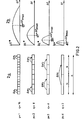
- FIG. 2 represents diagrams intended to illustrate the process of the invention when it takes place for example in 4 steps.
- E the error which we take the average
- the phase difference ⁇ 1 the frequency difference ⁇ f 1 by the relation
- the frequency deviation ⁇ f 3 can be estimated by calculating 3 errors E whose average value is taken.
- the measured frequency difference ⁇ f 3 is taken into account to correct the phase of the demodulated signal to be correlated with fractions of the synchronization word in the next step 4.
- the maximum measurable frequency difference is ⁇ f 4max -
- the frequency difference ⁇ f 4 is measured by calculating the error E from the two halves of the synchronization word.
- the measured frequency difference can be taken into account to correct the phase of the demodulated signal which, in a subsequent step which is not part of the frequency correction process proper, can be correlated with the whole.
- synchronization word in order to acquire frame synchronization and possibly sampling clock, as will be explained below.
- the frequency correction of the local carrier to be used is the sum of the 4 frequency deviations measured, ie ⁇ f 1 + ⁇ f 2 + Lf 3 + ⁇ f 4 .
- This frequency correction is actually used for the demodulation of the received signal, when the frame synchronization is acquired.
- the frequency correction device comprises a memory 12 which can be connected to the output of circuits 8 and 9 via the gate circuits 13 and 14 shown in the form of contacts. These gate circuits are controlled by a signal H 'supplied by 1 & sequencing circuit 29 to store in memory 12 each pair of samples S r and S i supplied by circuits 8 and 9.
- the sequencing circuit 29 receives pulses from the time base 11 and provides all the other control signals necessary for the operation of the device.
- the memory 12 is dimensioned to store pairs of samples S and S i in a number equal to the number n of bits of the synchronization word. These stored samples S, Si can be analog or digital depending on the technology used in the device.
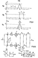
- the diagram 3a in FIG. 3 represents two consecutive pulses of the signal H 'which are separated by the period T from the sampling carried out in the circuits 8 and 9. Dn supposes for the moment that this period is the same as the period T modulation.
- the memory 12 receives a fast read clock signal h and having a sufficient frequency so that, during the period T, there appear at the two outputs of the memory as many sequences of n samples S and of n samples S i that it is necessary for the complete progress of the process.
- the signals x and y appearing at the two outputs of the memory 12 are the real and imaginary components of a complex signal z. They are applied to a phase rotation device 15 whose role is to rotate the phase of each sample in each sequence of n samples of the complex signal z, by a phase angle ⁇ VCD , corresponding to the frequency correction f VCD formed by the frequency correction device at the end of each step.
- the device 15 supplies the real and imaginary components X and Y of a complex signal Z, by performing the calculation:
- the quantities sin ⁇ VCD and cos ⁇ VCD used in the circuit 15 come from a read only memory 16 which is addressed by the phase ⁇ VCD supplied by the phase generator 17 at the rate of the fast clock h.
- the generator 17 prepares the phase ⁇ VCD from the frequency correction f VCD supplied by the frequency correction generator 18.
- the samples of the signals X and Y are applied to the correlation calculation circuits 19 and 20 to which are also applied samples of the real and imaginary components X 'and Y' of the local synchronization word.
- the n samples of each sequence of X 'and Y' are stored in the read-only memory 21 and read at fast clock rhythm h, each sequence being reproduced as many times as necessary for the complete progress of the process.
- the n samples X 'and Y' reproduce the phase states 6 K and the amplitude states corresponding to the n bits of the synchronization word transmitted; for phase modulation only (PSK type), the n samples X 'and Y' are simply cos ⁇ K and sin ⁇ K.
- the sampling signal H 1 shown in diagram 3b controls the reading, in circuits 19 and 20, of the results of the partial correlations, while the reset signal RESET 1 shown in diagram 3c resets the results of the correlations to zero. partial immediately after their reading by the signal H 1 .
- the period of the signals H 1 and RESET 1 defines the length of the synchronization word fractions used for the calculation of the partial correlations. As shown in Figure 3, this period is different depending on whether the process is in steps 1, 2, 3 or 4.
- the calculation circuits 19 and 20 respectively provide the partial correlation results C r (k) and C i (k), k defining the order of each partial correlation in each step.
- Diagram 3d shows that during step 1 are provided 16 results C (k), C i (k) numbered from 0 to 15, during step 2 are provided 8 results numbered from 0 to 7, during step 3 4 results are given numbered from 0 to 3 and during step 4 are provided 2 results C r (k) and C i (k) numbered 0 and 1.
- the successive results of the partial correlations are applied to the calculation circuit 22 which, from the pairs of consecutive partial correlations C r (k-1), C r (k) and C i (k-1), C i (k) generated at the rate of H 1 , calculates error terms E, according to expression (5) above.
- Each error term E depends on the phase difference ⁇ between the two consecutive fractions of the synchronization word used to provide the partial correlations C (k), C i (k) and C r (k-1), C i (k-1). As shown in diagram 3e, the calculated error terms correspond to phase differences ⁇ 1 during step 1, ⁇ 2 during step 2, ⁇ 3 during step 3 and finally to a phase difference ⁇ 4 during step 4.
- FIG. 11 intended to supplement FIG. 3, various control signals used in the device of the invention are shown.
- the diagram.lla intended to fix the time scale, represents like diagram 3a two consecutive pulses of the signal H ', which are separated by the sampling period T.
- This diagram lla also shows the periods of time during which take place steps 1, 2, 3 and 4.
- Diagrams llb and llc respectively represent the pulses of the sampling signal H 2 and of the reset signal RESET 2, these signals applied to circuit 23 exercising the functions described here above by means of pulses occurring at the end of steps 1, 2, 3 and 4.
- the average error terms generated in circuit 23 are applied to circuit 24 to be level corrected, so as to obtain corrected error terms E * ,, E * 2 , E * 3 , E * 4 practically equal to sin ⁇ 1 , sin ⁇ 2 , sin ⁇ 3 , sin ⁇ 4 .
- Diagram 3g shows that these quantities appear successively at the end of steps 1, 2, 3 and 4. '
- level corrected error terms are obtained by dividing the average error terms calculated in circuit 23 by the accumulation results formed as we have just explained in circuit 24. Corrected errors appear at the output of circuit 24 under the control of the sampling signal H 2 .
- the corrected errors E * are applied to circuit 25 whose role is to determine the frequency difference measured at the end of each step.
- this circuit first comprises means for determining the phase differences af as a function of the corrected errors E * .
- the circuit 25 determines the corresponding frequency deviations ⁇ f 1 , ⁇ f 2 , ⁇ f 3 , ⁇ f 4 using the relation (8) above. .
- the number of bits b to be taken into account for steps 1, 2, 3 and 4 is respectively , n being the total number of bits of the synchronization word.
- Diagram 3h shows the time intervals according to steps 1, 2, 3 and 4, during which the frequency deviations ⁇ f 1 , ⁇ f 2 , ⁇ f 3 , ⁇ f 4 are acquired.
- the frequency f VCD supplied by the circuit 18 is applied to the circuit 17 which supplies, at the rate of the fast clock h (used for reading the samples. X and y ions in the memory 12), the phase rotation ⁇ VCD to be applied to complex samples of components x and y.
- this phase rotation is zero during step 1, then after each of steps 1, 2, 3 and 4 increases from zero in proportion to ⁇ f 1 , ⁇ f 1 + ⁇ f 2 , ⁇ f 1 + ⁇ f 2 + ⁇ f 3 , ⁇ f 1 + ⁇ f 2 + ⁇ f 3 + ⁇ f 4 .
- the reset signal 4 applied to circuit 17 allows the proper resetting of ⁇ VCD , at the end of each step 1, 2, 3, 4. This reset signal 4 is shown in diagram llf.
- FIGs 4 to 7 show possible embodiments for the main circuits shown in Figure 1.
- the circuits and signals having the same functions have the same references in these figures.
- FIG. 4 shows an embodiment of the phase rotation device 15 and of the correlation calculation circuits 19 and 20.
- the device 15 comprises the multiplier circuits 30 to 33 and the combination circuits 34 and 35 arranged together to calculate the signals X and Y from the signals x and y and t quan- ities cos ⁇ and sin ⁇ VCD VCD, according to the formulas (9) given above.
- the correlation calculation circuits 19 and 20 are identical and operate in the same way.
- the circuit 19, for example, includes a multiplier circuit 36 which forms the product of the samples X supplied by the circuit 15 and of the samples X 'coming from the read-only memory 21.
- FIG. 5 shows an embodiment of the calculation circuit 22 of the error E and of the calculation circuit 23 of the average error E m .
- the circuit 22 receives the results of the partial correlations C (k) and C i (k). It includes memories 40 and 41 which store the previous results C r (k-1) and C i (k-1) and which, under the control of the sampling signal H 1 , restore the results of correlations C (k- 1) and C i (k-1) at the same time as the results of correlations C r (k) and C i (k) appear. All these correlation results are processed using the multiplier circuits 42, 43 and the combination circuit 44, arranged so as to calculate the error signal E according to the formula (5) indicated above.
- the averaging circuit 23 first comprises an accumulator which is formed of the adder circuit 45 and of the memory 46, which accumulates the error terms E applied to its input under the control of the sampling signal H 1 .
- the accumulator is reset to zero by the signal RESET 2 at the end of each step.
- the result of the accumulation, just before the reset of the accumulator is multiplied in the multiplier circuit 47 by the quantity , N m being the number of error terms accumulated in each stage.
- the result of the multiplication is supplied to the memory 48 which is read by the sampling signal of the mean error H2, so that the mean error terms of each step appear just after the end of each step.
- the circuit 24 which functions to correct the average error E m from the results of partial correlations C r (k) and C. (k) comprises the square elevation circuits 50 and 51 and the adder circuit 52 arranged to supply the quantity Quantities are accumulated in the accumulator formed by the adder circuit 53 and the memory 54. The accumulation is carried out at the rate of the sampling signal of the partial correlations H l ; at the end of each step, the memory 54 is reset to zero by the control signal RESET 2 .
- the output of the accumulator is connected to circuit 55 which forms the inverse value of the contents of the accumulator; this inverse value constitutes the correction factor C m to be applied to the mean error term E m .
- the factor C is supplied to the buffer memory 56, from which it is extracted therefrom by the control signal H 2 to be applied to the multiplier circuit 57 which also receives the average error E m read in the memory 48 by the same signal H 2 .
- the circuit 57 thus supplies the corrected error term E * .
- the circuit 25 which has the role of providing the frequency difference calculated at the end of each step, comprises for example a read only memory 58 in which the phase differences ⁇ are read at addresses formed by the corrected errors E * .
- FIG. 7 shows embodiments of circuits 18 and 17.
- Circuit 18 comprises an accumulator which is constituted by the adder circuit 60 and memory 61 and which accumulates under the control of the sampling signal H 3 the quantities ⁇ T formed at the outcome of the process steps.
- the memory 61 is reset to zero by the signal RESET 3 at the end of each period T so that its content is zero at the start of the following period.
- the output of the accumulator of circuit 18 thus produces the quantity ⁇ VCD T proportional to the frequency correction f VCD .
- the circuit 17 includes an accumulator which is constituted by the adder circuit 62 and the memory 63 and which accumulates the quantities ⁇ VCD T at the rate of the fast clock h.
- the memory 63 is reset to zero by the signal RESET 4 at the end of each step.
- the output of the accumulator simulates the phase rotation VCD to be applied to the complex samples of components x and y to compensate for the frequency difference of the local carrier with respect to the received carrier.
- the partial correlations for steps 2, 3, 4 are determined from the partial correlations calculated during the first step, which remain formed from the n pairs. of samples x and y read in memory 12 and of the n pairs of samples X 'and Y' read in memory 21. In these steps 2, 3, 4, these n pairs of samples are therefore reread memories 12 and 21.
- the method used to obtain the partial correlations for steps 2, 3, 4 consists in adding two by two the partial correlations calculated respectively during the preceding steps 1, 2, 3. But before making this addition, it is necessary to carry out beforehand phase correction of the partial correlations calculated during the previous phases, using the frequency deviation which has just been estimated.
- FIG. 8 shows how this variant of the process of the invention can be implemented, while for its operation one can use the diagrams already described in FIGS. 3 and 11, as supplemented by diagrams llg, llh and lli of figure 11.
- the elements having the same functions as in Figure 1 are provided with the same references.
- the memory 12 which, as explained, receives at each period T a pair of samples S, S. via the gates 13 and 14, and which has a capacity of n pairs of samples.
- the samples x, y read in the memory 12 at the rate of the fast clock h are applied directly to the correlation calculation circuits 19 and 20, at the same time as the n pairs of samples X ', Y' of the synchronization word local, which are also read at the rate of the clock h.
- the control signals H l and RESET 1 identical to those used in the diagram of FIG.
- circuits 19 and 20 are connected to the circuit 22 for calculating the error E, only during step 1, thanks to the switching circuits 70 and 71 established in the appropriate position by the control signal H 4 shown in the diagram llg.
- the output of circuits 19 and 20 is also connected to the inputs of memory 72, via the switch circuit 73 also controlled by the control signal H 4 , so that memory 72 stores the partial correlations developed during step 1.
- the partial correlations developed during step 1 are used to calculate, as explained for the variant of FIG. 1, the errors E 1 in circuit 22, then the average error E 1m in circuit 23.
- the 16 partial correlations calculated during step 1 and stored in memory 72, are read there during step 2 by the control signal H 5 represented in the diagram 11h. They are used in the correction circuit 24 having the same function as that of FIG. 1, to correct the average error E 1m which also appears during step 2.
- the 16 pairs of partial correlations of step 1, read in memory 72 are also applied to the circuit of phase rotation 74 to be corrected by phase ⁇ VCD
- the latter provides trains of partial correlations corrected in phase C and C by performing the calculations:
- the quantities sin ⁇ VCD and cos ⁇ VCD are read from the read-only memory 16 by means of the phase ⁇ ' VCD developed by the phase generator 75.
- the latter consists of an accumulator which is formed by the adder circuit 76 and the memory 77 , which accumulates, at the rate of the control signal H 5 , the phase differences ⁇ supplied by the circuit 58 and which is reset to zero by the signal RESET 4 at the end of each step.
- the 16 pairs of partial correlations applied during step 2 to the phase rotation circuit 74 there are corrected in phase by the phase ⁇ ' VCO1 constituted by the accumulation of the phase difference ⁇ 1 .
- Each pair of the 16 partial correlations corrected by the phase ⁇ VCD1 is applied to the adder circuits 78, 79 to be added to the previous pair of partial correlations extracted from the memories 80 and 81 using the control signal H 5 .
- the sums supplied 'at the output of circuits 78 and 79 are written into memory 82 by the control signal H 6 which is represented on the diagram lli and which has a rhythm half of the control signal H 5 , so that this memory 82 stores the 8 pairs of partial correlations developed during step 2, from the 16 pairs of partial correlations of step 1.
- step 2 These 8 pairs of partial correlations of step 2 are read from memory 82 at the rate of the control signal H 6 and are applied on the one hand, via the switching circuits 70 and 71, to circuit 22 which calculates the 8 errors E 2 of step 2 and on the other hand, via the switch circuit 73, to the memory 72 to be stored there until their next reading by the control signal H 5 during step 3.
- step 3 the process already described for step 2 is reproduced: calculation of the average error E2m, of the corrected error E * 2 , of the phase difference ⁇ 2 , of the phase ⁇ VCD2 which is used to correct in phase the 8 partial correlations read from memory 72, and finally calculation of the sums two by two of the corrected partial correlations; four of these sums are written to memory 82 and are used in the same way.
- step 4 the phase difference ⁇ 3 and the phase ⁇ VCD3 also used to correct in phase the 4 partial correlations read from memory 72. Finally, during this step 4 are written to memory 82 two pairs of partial correlations corrected in phase.
- phase difference ⁇ 4 can be used to calculate the phase ⁇ ' VCD4 used to correct in phase the two partial correlations read from memory 72 and form in memory 82 a complete correlation, corrected in phase, between the local synchronization word and the received signal demodulated. As already indicated, this full correlation can be used for sampling clock synchronization and frame synchronization.
- the phases ⁇ ' VCD1 , ⁇ ' VCD2 ⁇ 'VCD 3 ⁇ 'VCD 4 used to correct in phase the partial correlations of each step 1, 2, 3 and 4 are obtained directly from the calculated phase differences ⁇ 1 , ⁇ 2 ⁇ 3 , ⁇ 4
- the phases used to correct the samples read in the memory 12 are obtained from the cumulative frequency differences, let ⁇ f 1 , ⁇ f 1 + ⁇ f 2 , ⁇ f 1 + ⁇ f 2 + ⁇ f 3 , ⁇ f 1 + ⁇ f 2 + ⁇ f 3 + ⁇ f 4 .
- the device of FIG. 8 must be provided with means for developing this frequency f VCD .
- the phase differences ⁇ supplied by the circuit 58 are treated as explained using FIGS. 6 and 7.
- the quantities ⁇ T proportional to the frequency deviations ⁇ f, are accumulated in the circuit 18 which provides at the end of step 4 the quantity ⁇ VCD T proportional to the frequency correction f VCD .
- diagram 9a the complete correlation function C, determined from continuously, assuming clock synchronization is acquired.
- the correlation function C presents a peak, at one of the instants of the sampling clock of period T, indicated by the graduations of the time axis.
- the function C has the value 1 at time t of this peak and the value - , if for example the synchronization word is a so-called maximum length sequence.
- the instant t of the peak indicates the instant when the n previous samples of the received signal constitute the synchronization word transmitted.
- Diagram 9b represents the complete correlation C determined from the sampled signals with the period T of the sampling clock, as actually occurs in the device of the invention. As it is assumed in diagram 9b that the synchronization of the clock is acquired, the time t 0 of the correlation peak is rigorously obtained by comparing the correlation Ce obtained from sampled signals with a threshold S e .
- the frequency correction device can be identical, but work in time distribution on j signals sampled with period T and interleaved to reach the end of the frequency correction process to j frequency correction values f VCD and finally to j complete correlations corresponding respectively to said j interlaced signals.
- Diagram 9c shows the correlation Ces which is the image of the correlation function C of diagram 9a and which is obtained with a sampling frequency .
- the sampling clock and frame synchronization search processes that have just been explained can be implemented using the correlation calculation means of the devices in FIGS. 1 and 8.
- the real and imaginary components Ci and C complete correlations which can be obtained after the frequency search process are for example applied to circuits squaring them, the quantities squared obtained are applied to an adder circuit which forms a sum which is compared to a threshold, the instant when this threshold is exceeded, providing frame synchronization and sampling clock synchronization.
- phase rotation device 15 the samples tillons of components S r , S i are corrected in phase, using components sin ⁇ VCD and cos ⁇ VCD read from memory 16 using the phase ⁇ VCD and developed in phase generator 85.
- the device 15 of phase rotation provides samples e, e i resulting from a calculation analogous to that indicated by the formulas (9).
- This phase ⁇ VCD is obtained using an accumulator, constituted by the adder circuit 86 and the memory 87.
- the frequency f VCD (or a proportional quantity) stored in memory 88, is accumulated with the accumulation frequency , from the initial instant t o determined by the signal RESET O.
- the corrected samples e r , e i supplied by the phase rotation circuit 15 are applied to the decision circuit 89 which restores the data D.
- the frequency f VCD could moreover be controlled using 'A control loop allowing the synchronization of the carrier to be maintained and having no link with the device of the invention which is only used for the acquisition of this synchronization.
Landscapes
- Engineering & Computer Science (AREA)
- Computer Networks & Wireless Communication (AREA)
- Signal Processing (AREA)
- Synchronisation In Digital Transmission Systems (AREA)
- Digital Transmission Methods That Use Modulated Carrier Waves (AREA)
Applications Claiming Priority (2)
| Application Number | Priority Date | Filing Date | Title |
|---|---|---|---|
| FR8206289A FR2525055A1 (fr) | 1982-04-09 | 1982-04-09 | Procede de correction de frequence de la porteuse locale dans le recepteur d'un systeme de transmission de donnees et recepteur utilisant ce procede |
| FR8206289 | 1982-04-09 |
Publications (2)
| Publication Number | Publication Date |
|---|---|
| EP0091167A1 true EP0091167A1 (de) | 1983-10-12 |
| EP0091167B1 EP0091167B1 (de) | 1986-01-02 |
Family
ID=9272965
Family Applications (1)
| Application Number | Title | Priority Date | Filing Date |
|---|---|---|---|
| EP83200461A Expired EP0091167B1 (de) | 1982-04-09 | 1983-03-31 | Verfahren zur Frequenzkorrektur des lokalen Trägers im Empfänger eines Datenübertragungssystems und Empfänger unter Verwendung dieses Verfahrens |
Country Status (8)
| Country | Link |
|---|---|
| US (1) | US4527278A (de) |
| EP (1) | EP0091167B1 (de) |
| JP (1) | JPH0638611B2 (de) |
| AU (1) | AU556701B2 (de) |
| CA (1) | CA1211794A (de) |
| DE (1) | DE3361666D1 (de) |
| FR (1) | FR2525055A1 (de) |
| NO (1) | NO831221L (de) |
Cited By (15)
| Publication number | Priority date | Publication date | Assignee | Title |
|---|---|---|---|---|
| EP0155776A1 (de) * | 1984-03-01 | 1985-09-25 | Stc Plc | Digitaler NAVSTAR-Empfänger |
| EP0186691A4 (de) * | 1984-04-17 | 1986-07-24 | Harris Corp | Technik zur erreichung von takt- und frequenzsynchronisation für modem, das bekannte (nichtdaten) symbole als teil ihrer normalerweise übertragenen daten verwendet. |
| EP0149546A3 (de) * | 1984-01-13 | 1987-10-14 | Asea Brown Boveri Inc. | Empfänger für Netzleitungsübertragungssysteme |
| EP0257584A1 (de) * | 1986-08-21 | 1988-03-02 | Nec Corporation | Trägerrückgewinnungsschaltung, die gegen Interburst-Frequenzveränderungen unempfindlich ist |
| GB2203303A (en) * | 1987-03-31 | 1988-10-12 | Stc Plc | Radio frequency tracking loop |
| GB2207582A (en) * | 1987-07-30 | 1989-02-01 | Stc Plc | Phase error correction and carrier recovery |
| FR2633471A1 (fr) * | 1988-06-28 | 1989-12-29 | Trt Telecom Radio Electr | Procede de demodulation coherente d'un signal module numeriquement en phase continue et a enveloppe constante |
| EP0389974A1 (de) * | 1989-03-31 | 1990-10-03 | Motorola, Inc. | Vorrichtung und Verfahren zur Frequenzsteuerung für einen digitalen Funkempfänger |
| EP0410532A1 (de) * | 1989-07-28 | 1991-01-30 | Telecommunications Radioelectriques Et Telephoniques T.R.T. | Verfahren zum Synchronisieren durch Korrelation |
| EP0455140A1 (de) * | 1990-05-04 | 1991-11-06 | Alcatel Mobile Communication France | Einrichtung zur Schätzung der Frequenzverschiebung |
| EP0427283A3 (en) * | 1989-11-10 | 1992-03-25 | Nec Corporation | Fast psk carrier recovery in a mobile satellite communication network |
| EP0454266A3 (en) * | 1990-04-26 | 1992-09-30 | Philips Patentverwaltung | Receiver comprising a circuit for estimating frequency offset |
| EP0535591A3 (en) * | 1991-09-30 | 1993-05-12 | Nec Corporation | Phase-locked circuit capable of being quickly put in a phase locked state |
| EP0551081A3 (en) * | 1992-01-10 | 1994-05-11 | Mitsubishi Electric Corp | Adaptive equalizer and receiver |
| EP0757462A3 (de) * | 1995-08-04 | 2000-09-06 | Matsushita Electric Industrial Co., Ltd. | Korrektur eine Frequenzverschiebung für ein Datenempfangssystem |
Families Citing this family (41)
| Publication number | Priority date | Publication date | Assignee | Title |
|---|---|---|---|---|
| GB2153177B (en) * | 1984-01-19 | 1987-06-03 | Standard Telephones Cables Ltd | Digital navstar receiver |
| JPH0821962B2 (ja) * | 1984-03-02 | 1996-03-04 | 日本電信電話株式会社 | キヤリアトラツキング回路 |
| GB2181907B (en) * | 1985-10-18 | 1989-10-11 | Stc Plc | Phase rotation of signals |
| JP2632707B2 (ja) * | 1988-07-30 | 1997-07-23 | 三菱プレシジョン株式会社 | デモジュレーション装置 |
| US5027352A (en) * | 1989-01-05 | 1991-06-25 | Motorola, Inc. | Receiver frequency offset bias circuit for TDM radios |
| SE462943B (sv) * | 1989-01-26 | 1990-09-17 | Ericsson Telefon Ab L M | Saett och anordning foer frekvensstyrning av en koherent radiomottagare |
| US5001727A (en) * | 1989-02-15 | 1991-03-19 | Terra Marine Engineering, Inc. | Carrier and data recovery and demodulation system |
| US4943982A (en) * | 1989-05-01 | 1990-07-24 | Motorola, Inc. | Baseband carrier phase corrector |
| US5241702A (en) * | 1990-09-06 | 1993-08-31 | Telefonaktiebolaget L M Ericsson | D.c. offset compensation in a radio receiver |
| US5123033A (en) * | 1990-09-27 | 1992-06-16 | At&T Bell Laboratories | Extraction of an exact symbol rate as applied to bandwidth compression of modem signals through demodulation and remodulation |
| US5297172A (en) * | 1991-04-11 | 1994-03-22 | Comsat Corporation | Method and apparatus for clock recovery for digitally implemented modem |
| IT1259013B (it) * | 1992-07-27 | 1996-03-11 | Alcatel Italia | Sistema demodulatore completamente digitale per segnalazioni qam in collegamenti di piccola capacita' |
| US5376894A (en) * | 1992-12-31 | 1994-12-27 | Pacific Communication Sciences, Inc. | Phase estimation and synchronization using a PSK demodulator |
| JPH07212421A (ja) * | 1994-01-19 | 1995-08-11 | Toshiba Corp | Afc回路 |
| EP0674412B1 (de) * | 1994-03-25 | 2004-07-14 | Samsung Electronics Co., Ltd. | Verfahren und Vorrichtung für automatische Frequenzregelung |
| DE4423763C1 (de) * | 1994-06-28 | 1996-02-01 | Siemens Ag | Verfahren zum digitalen Bestimmen des Effektivwertes eines periodischen elektrischen Meßsignals |
| US5909471A (en) * | 1997-08-08 | 1999-06-01 | Arraycomm, Inc. | Method and system for rapid initial control signal detection in a wireless communications system |
| GB2344493A (en) * | 1998-09-12 | 2000-06-07 | Roke Manor Research | Automatic frequency correction |
| JP3252820B2 (ja) | 1999-02-24 | 2002-02-04 | 日本電気株式会社 | 復調及び変調回路並びに復調及び変調方法 |
| GB2358116B (en) * | 1999-02-24 | 2002-11-06 | Nec Corp | Demodulation circuit and demodulation method with compensation for sampling offset |
| US9020756B2 (en) * | 1999-04-23 | 2015-04-28 | Global Locate, Inc. | Method and apparatus for processing satellite positioning system signals |
| US6704348B2 (en) | 2001-05-18 | 2004-03-09 | Global Locate, Inc. | Method and apparatus for computing signal correlation at multiple resolutions |
| US6606346B2 (en) * | 2001-05-18 | 2003-08-12 | Global Locate, Inc. | Method and apparatus for computing signal correlation |
| JP3486576B2 (ja) | 1999-05-18 | 2004-01-13 | シャープ株式会社 | Ofdm受信装置及びその周波数オフセット補償方法 |
| US6426982B1 (en) | 1999-09-17 | 2002-07-30 | Cadonca Design Systems, Inc. | Low complexity multiple bits matched filter |
| US6532271B1 (en) | 1999-10-29 | 2003-03-11 | Cadence Design Systems, Inc. | Carrier recovery and doppler frequency estimation |
| US6606363B1 (en) * | 1999-12-28 | 2003-08-12 | Telefonaktiebolaget Lm Ericsson (Publ) | Method and apparatus for estimating a frequency offset by combining pilot symbols and data symbols |
| US7567636B2 (en) * | 2001-05-18 | 2009-07-28 | Global Locate, Inc. | Method and apparatus for performing signal correlation using historical correlation data |
| US7190712B2 (en) * | 2001-05-18 | 2007-03-13 | Global Locate, Inc | Method and apparatus for performing signal correlation |
| US6891880B2 (en) * | 2001-05-18 | 2005-05-10 | Global Locate, Inc. | Method and apparatus for performing signal correlation |
| US6819707B2 (en) | 2001-05-18 | 2004-11-16 | Global Locate, Inc. | Method and apparatus for performing signal correlation using historical correlation data |
| US7995682B2 (en) * | 2001-05-18 | 2011-08-09 | Broadcom Corporation | Method and apparatus for performing signal processing using historical correlation data |
| US7006556B2 (en) * | 2001-05-18 | 2006-02-28 | Global Locate, Inc. | Method and apparatus for performing signal correlation at multiple resolutions to mitigate multipath interference |
| US7769076B2 (en) * | 2001-05-18 | 2010-08-03 | Broadcom Corporation | Method and apparatus for performing frequency synchronization |
| US8098716B2 (en) * | 2001-05-18 | 2012-01-17 | Broadcom Corporation | Method and apparatus for providing an energy-based signal tracking loop |
| AU2002349638A1 (en) * | 2001-11-20 | 2003-06-10 | Sanyo Electric Co., Ltd. | Radio reception apparatus, symbol timing control method, and symbol timing control program |
| US7443935B2 (en) * | 2002-11-02 | 2008-10-28 | Texas Instruments Incorporated | Apparatus and method for dynamically adjusting receiver bandwidth |
| JP2005303928A (ja) * | 2004-04-15 | 2005-10-27 | Fujitsu Ltd | 分割加算式マッチトフィルタシステム |
| DE102005019177B4 (de) * | 2005-04-25 | 2010-02-11 | Infineon Technologies Ag | Verfahren und Vorrichtung zur Frequenzschätzung bei der Akquistition eines Spreizcode-Signals |
| US7630428B2 (en) * | 2005-07-28 | 2009-12-08 | Itt Manufacturing Enterprises, Inc. | Fast digital carrier frequency error estimation algorithm using synchronization sequence |
| TW200803389A (en) * | 2006-06-20 | 2008-01-01 | Nxp Bv | Method and apparatus for estimating carrier frequency offset |
Citations (3)
| Publication number | Priority date | Publication date | Assignee | Title |
|---|---|---|---|---|
| US3962637A (en) * | 1974-11-11 | 1976-06-08 | Hycom Incorporated | Ultrafast adaptive digital modem |
| US3971996A (en) * | 1973-01-18 | 1976-07-27 | Hycom Incorporated | Phase tracking network |
| FR2342595A1 (fr) * | 1976-02-28 | 1977-09-23 | Licentia Gmbh | Procede de transmission d'information pour voies presentant une distorsion lineaire avec des decalages de frequence |
Family Cites Families (5)
| Publication number | Priority date | Publication date | Assignee | Title |
|---|---|---|---|---|
| US3447085A (en) * | 1965-01-04 | 1969-05-27 | Gen Dynamics Corp | Synchronization of receiver time base in plural frequency differential phase shift system |
| DE2358288A1 (de) * | 1973-11-22 | 1975-06-05 | Standard Elektrik Lorenz Ag | Empfaenger fuer frequenzmodulierte hf-signale |
| DE2657914C2 (de) * | 1976-12-21 | 1978-11-30 | Siemens Ag, 1000 Berlin Und 8000 Muenchen | Schaltungsanordnung zum Grobsynchronisieren von Trägersignalen und Taktsignalen mit Datensignalen in einem Datenempfänger |
| US4328587A (en) * | 1979-02-19 | 1982-05-04 | Kokusai Denshin Denwa Kabushiki Kaisha | Phase slip detector and systems employing the detector |
| DE2913172B2 (de) * | 1979-04-02 | 1981-06-11 | Siemens AG, 1000 Berlin und 8000 München | Empfänger für hochfrequente elektromagneitsche Schwingungen mit einer Frequenznachregelung |
-
1982
- 1982-04-09 FR FR8206289A patent/FR2525055A1/fr active Granted
-
1983
- 1983-03-31 DE DE8383200461T patent/DE3361666D1/de not_active Expired
- 1983-03-31 EP EP83200461A patent/EP0091167B1/de not_active Expired
- 1983-04-06 CA CA000425288A patent/CA1211794A/en not_active Expired
- 1983-04-06 NO NO831221A patent/NO831221L/no unknown
- 1983-04-06 AU AU13173/83A patent/AU556701B2/en not_active Ceased
- 1983-04-07 US US06/483,085 patent/US4527278A/en not_active Expired - Lifetime
- 1983-04-09 JP JP58061574A patent/JPH0638611B2/ja not_active Expired - Lifetime
Patent Citations (3)
| Publication number | Priority date | Publication date | Assignee | Title |
|---|---|---|---|---|
| US3971996A (en) * | 1973-01-18 | 1976-07-27 | Hycom Incorporated | Phase tracking network |
| US3962637A (en) * | 1974-11-11 | 1976-06-08 | Hycom Incorporated | Ultrafast adaptive digital modem |
| FR2342595A1 (fr) * | 1976-02-28 | 1977-09-23 | Licentia Gmbh | Procede de transmission d'information pour voies presentant une distorsion lineaire avec des decalages de frequence |
Non-Patent Citations (1)
| Title |
|---|
| IBM TECHNICAL DISCLOSURE BULLETIN, vol. 15, no. 1, juin 1972, pages 81-83, New York, USA * |
Cited By (22)
| Publication number | Priority date | Publication date | Assignee | Title |
|---|---|---|---|---|
| EP0149546A3 (de) * | 1984-01-13 | 1987-10-14 | Asea Brown Boveri Inc. | Empfänger für Netzleitungsübertragungssysteme |
| EP0155776A1 (de) * | 1984-03-01 | 1985-09-25 | Stc Plc | Digitaler NAVSTAR-Empfänger |
| EP0186691A4 (de) * | 1984-04-17 | 1986-07-24 | Harris Corp | Technik zur erreichung von takt- und frequenzsynchronisation für modem, das bekannte (nichtdaten) symbole als teil ihrer normalerweise übertragenen daten verwendet. |
| EP0257584A1 (de) * | 1986-08-21 | 1988-03-02 | Nec Corporation | Trägerrückgewinnungsschaltung, die gegen Interburst-Frequenzveränderungen unempfindlich ist |
| GB2203303B (en) * | 1987-03-31 | 1991-02-13 | Stc Plc | Radio frequency tracking loop |
| GB2203303A (en) * | 1987-03-31 | 1988-10-12 | Stc Plc | Radio frequency tracking loop |
| GB2207582A (en) * | 1987-07-30 | 1989-02-01 | Stc Plc | Phase error correction and carrier recovery |
| GB2207582B (en) * | 1987-07-30 | 1991-04-24 | Stc Plc | Phase error correction and carrier recovery |
| FR2633471A1 (fr) * | 1988-06-28 | 1989-12-29 | Trt Telecom Radio Electr | Procede de demodulation coherente d'un signal module numeriquement en phase continue et a enveloppe constante |
| EP0349064A1 (de) * | 1988-06-28 | 1990-01-03 | Telecommunications Radioelectriques Et Telephoniques T.R.T. | Verfahren zur Demodulation eines mit kontinuierlicher Phase und konstanter Umhüllung digital-modulierten Signals |
| EP0389974A1 (de) * | 1989-03-31 | 1990-10-03 | Motorola, Inc. | Vorrichtung und Verfahren zur Frequenzsteuerung für einen digitalen Funkempfänger |
| FR2650456A1 (fr) * | 1989-07-28 | 1991-02-01 | Trt Telecom Radio Electr | Procede de synchronisation par correlation |
| EP0410532A1 (de) * | 1989-07-28 | 1991-01-30 | Telecommunications Radioelectriques Et Telephoniques T.R.T. | Verfahren zum Synchronisieren durch Korrelation |
| EP0427283A3 (en) * | 1989-11-10 | 1992-03-25 | Nec Corporation | Fast psk carrier recovery in a mobile satellite communication network |
| AU627380B2 (en) * | 1989-11-10 | 1992-08-20 | Nec Corporation | Carrier regenerating device correctly operable in mobile satellite communication |
| EP0454266A3 (en) * | 1990-04-26 | 1992-09-30 | Philips Patentverwaltung | Receiver comprising a circuit for estimating frequency offset |
| EP0455140A1 (de) * | 1990-05-04 | 1991-11-06 | Alcatel Mobile Communication France | Einrichtung zur Schätzung der Frequenzverschiebung |
| FR2661792A1 (fr) * | 1990-05-04 | 1991-11-08 | Alcatel Radiotelephone | Dispositif d'evaluation d'ecart de frequence. |
| AU642240B2 (en) * | 1990-05-04 | 1993-10-14 | Alcatel N.V. | Circuit for evaluating frequency difference |
| EP0535591A3 (en) * | 1991-09-30 | 1993-05-12 | Nec Corporation | Phase-locked circuit capable of being quickly put in a phase locked state |
| EP0551081A3 (en) * | 1992-01-10 | 1994-05-11 | Mitsubishi Electric Corp | Adaptive equalizer and receiver |
| EP0757462A3 (de) * | 1995-08-04 | 2000-09-06 | Matsushita Electric Industrial Co., Ltd. | Korrektur eine Frequenzverschiebung für ein Datenempfangssystem |
Also Published As
| Publication number | Publication date |
|---|---|
| FR2525055B1 (de) | 1984-05-04 |
| JPH0638611B2 (ja) | 1994-05-18 |
| EP0091167B1 (de) | 1986-01-02 |
| JPS58187046A (ja) | 1983-11-01 |
| FR2525055A1 (fr) | 1983-10-14 |
| US4527278A (en) | 1985-07-02 |
| AU1317383A (en) | 1983-10-13 |
| CA1211794A (en) | 1986-09-23 |
| AU556701B2 (en) | 1986-11-13 |
| NO831221L (no) | 1983-10-10 |
| DE3361666D1 (en) | 1986-02-13 |
Similar Documents
| Publication | Publication Date | Title |
|---|---|---|
| EP0091167B1 (de) | Verfahren zur Frequenzkorrektur des lokalen Trägers im Empfänger eines Datenübertragungssystems und Empfänger unter Verwendung dieses Verfahrens | |
| US5590158A (en) | Method and apparatus for estimating PSK modulated signals | |
| EP0513313B1 (de) | Verfahren zur neusynchronisierung der lokalen oszillatoren eines empfängers und vorrichtung zur durchführung des verfahrens | |
| EP0877487B1 (de) | Kohärenter, Fraktional-N-Frequenzsynthetisierer mit einer Phasenregelschleife | |
| CH668675A5 (fr) | Modulateur de phases multiples, demodulateur, modem les comprenant et installation de transmission. | |
| EP0410532B1 (de) | Verfahren zum Synchronisieren durch Korrelation | |
| EP0116387B1 (de) | Verfahren zur Anfangseinstellung der Filterkoeffizienten in einer Anordnung zur Kompensation naher und ferner Echos, sowie Vorrichtung zur Durchführung dieses Verfahrens | |
| FR2770700A1 (fr) | Dispositif et procede pour synchroniser des oscillateurs dans un systeme de communication de donnees | |
| EP0018242B1 (de) | Im Zeitmultiplex auf mehreren Kanälen arbeitendes Verfahren und Vorrichtung zur stochastischen Demodulation phasensprungmodulierter Signale | |
| EP1041729A1 (de) | Verfahren zur Taktsynchronisierung eines digitalen Signals | |
| EP0003943B1 (de) | Verfahren und Einrichtung zur Bestimmung der Taktanfangsphase in einem synchronen Datenempfänger | |
| EP0352159B1 (de) | Frequenzabweichungstolerierendes Verfahren und Vorrichtung zur Demodulation von, durch eine Binärsymbolreihe, winkelmodulierten Signalen mit konstanter Umhüllung und kontinuierlicher Phase | |
| JP2002335294A (ja) | 曲線当てはめによる位相同期ループ初期化 | |
| FR2623352A1 (de) | ||
| CA2206946A1 (fr) | Systeme de detection de la presence d'une onde porteuse d'un signal numerique et recepteur comprenant un tel systeme | |
| EP0035295B1 (de) | Verfahren zur Regelung der Phase des Taktgenerators eines Empfangssystems für digitale Daten, Phasenrückgewinnungsschaltung zur Durchführung dieses Verfahrens und Empfangssystem für digitale Daten mit dieser Schaltung | |
| EP0094040B1 (de) | System zur synchronen Datenübertragung mit Hilfe eines amplitudenmodulierten Trägers konstanter Hüllkurve | |
| EP0498704B1 (de) | Verfahren zur kohärenten PSK-Demodulation und Einrichtung zu dessen Ausführung | |
| FR2786965A1 (fr) | Procede de recuperation de porteuse de signal | |
| EP0723354A1 (de) | Erzeugung von Quadraturträgern für Demodulierung | |
| EP1142147B1 (de) | Verfahren zum empfangen von spreizspektrumsignalen mit korrektur des frequenzversatzes | |
| EP0607063A1 (de) | Einrichtung zur Korrektur von Phasenfehlern, für PSK-Signale, die in Paketen übertragen werden | |
| EP0648037A1 (de) | Phasenabgleich im Basisband | |
| EP0137553B1 (de) | Digitales Demodulationsverfahren und Schaltung für ein amplitudenmoduliertes Signal und eine solche Schaltung enthaltender Fernsehempfänger | |
| EP0045260A1 (de) | Demodulator für mittels stetiger Phasen-Modulation modulierte Signale und einen solchen Demodulator enthaltendes Übertragungssystem |
Legal Events
| Date | Code | Title | Description |
|---|---|---|---|
| PUAI | Public reference made under article 153(3) epc to a published international application that has entered the european phase |
Free format text: ORIGINAL CODE: 0009012 |
|
| AK | Designated contracting states |
Designated state(s): DE FR GB IT SE |
|
| 17P | Request for examination filed |
Effective date: 19831104 |
|
| GRAA | (expected) grant |
Free format text: ORIGINAL CODE: 0009210 |
|
| AK | Designated contracting states |
Designated state(s): DE FR GB IT SE |
|
| REF | Corresponds to: |
Ref document number: 3361666 Country of ref document: DE Date of ref document: 19860213 |
|
| ITF | It: translation for a ep patent filed | ||
| PLBE | No opposition filed within time limit |
Free format text: ORIGINAL CODE: 0009261 |
|
| STAA | Information on the status of an ep patent application or granted ep patent |
Free format text: STATUS: NO OPPOSITION FILED WITHIN TIME LIMIT |
|
| 26N | No opposition filed | ||
| PGFP | Annual fee paid to national office [announced via postgrant information from national office to epo] |
Ref country code: FR Payment date: 19930326 Year of fee payment: 11 |
|
| ITTA | It: last paid annual fee | ||
| PG25 | Lapsed in a contracting state [announced via postgrant information from national office to epo] |
Ref country code: FR Effective date: 19941130 |
|
| REG | Reference to a national code |
Ref country code: FR Ref legal event code: ST |
|
| EAL | Se: european patent in force in sweden |
Ref document number: 83200461.8 |
|
| ITPR | It: changes in ownership of a european patent |
Owner name: CAMBIO RAGIONE SOCIALE;PHILIPS ELECTRONICS N.V. |
|
| PGFP | Annual fee paid to national office [announced via postgrant information from national office to epo] |
Ref country code: SE Payment date: 19970425 Year of fee payment: 15 |
|
| PGFP | Annual fee paid to national office [announced via postgrant information from national office to epo] |
Ref country code: DE Payment date: 19970523 Year of fee payment: 15 |
|
| PGFP | Annual fee paid to national office [announced via postgrant information from national office to epo] |
Ref country code: GB Payment date: 19980302 Year of fee payment: 16 |
|
| PG25 | Lapsed in a contracting state [announced via postgrant information from national office to epo] |
Ref country code: SE Free format text: LAPSE BECAUSE OF NON-PAYMENT OF DUE FEES Effective date: 19980401 |
|
| PG25 | Lapsed in a contracting state [announced via postgrant information from national office to epo] |
Ref country code: DE Free format text: LAPSE BECAUSE OF NON-PAYMENT OF DUE FEES Effective date: 19981201 |
|
| EUG | Se: european patent has lapsed |
Ref document number: 83200461.8 |
|
| PG25 | Lapsed in a contracting state [announced via postgrant information from national office to epo] |
Ref country code: GB Free format text: LAPSE BECAUSE OF NON-PAYMENT OF DUE FEES Effective date: 19990331 |
|
| GBPC | Gb: european patent ceased through non-payment of renewal fee |
Effective date: 19990331 |