EP0111201B1 - Tube à mémoire à balayage à cible à collecteur multiple et méthode de fonctionnement - Google Patents
Tube à mémoire à balayage à cible à collecteur multiple et méthode de fonctionnement Download PDFInfo
- Publication number
- EP0111201B1 EP0111201B1 EP83111624A EP83111624A EP0111201B1 EP 0111201 B1 EP0111201 B1 EP 0111201B1 EP 83111624 A EP83111624 A EP 83111624A EP 83111624 A EP83111624 A EP 83111624A EP 0111201 B1 EP0111201 B1 EP 0111201B1
- Authority
- EP
- European Patent Office
- Prior art keywords
- storage
- collector
- collector electrodes
- group
- surface portions
- Prior art date
- Legal status (The legal status is an assumption and is not a legal conclusion. Google has not performed a legal analysis and makes no representation as to the accuracy of the status listed.)
- Expired
Links
- 238000003860 storage Methods 0.000 title claims description 431
- 238000000034 method Methods 0.000 title claims description 31
- 239000000758 substrate Substances 0.000 claims description 50
- 238000010894 electron beam technology Methods 0.000 claims description 48
- 230000037452 priming Effects 0.000 claims description 9
- 229910052594 sapphire Inorganic materials 0.000 claims description 8
- 239000010980 sapphire Substances 0.000 claims description 8
- VYPSYNLAJGMNEJ-UHFFFAOYSA-N Silicium dioxide Chemical compound O=[Si]=O VYPSYNLAJGMNEJ-UHFFFAOYSA-N 0.000 claims description 6
- 239000011810 insulating material Substances 0.000 claims description 6
- 239000013078 crystal Substances 0.000 claims description 4
- 239000000377 silicon dioxide Substances 0.000 claims description 4
- 235000012239 silicon dioxide Nutrition 0.000 claims description 4
- 230000003252 repetitive effect Effects 0.000 claims description 3
- 229910021421 monocrystalline silicon Inorganic materials 0.000 claims description 2
- 229910021420 polycrystalline silicon Inorganic materials 0.000 claims description 2
- 230000009977 dual effect Effects 0.000 description 12
- 230000004048 modification Effects 0.000 description 7
- 238000012986 modification Methods 0.000 description 7
- 230000008901 benefit Effects 0.000 description 6
- 238000010276 construction Methods 0.000 description 5
- 239000003990 capacitor Substances 0.000 description 4
- 238000010586 diagram Methods 0.000 description 4
- 239000012212 insulator Substances 0.000 description 4
- 238000004519 manufacturing process Methods 0.000 description 4
- 238000005520 cutting process Methods 0.000 description 3
- 239000012634 fragment Substances 0.000 description 3
- 239000011521 glass Substances 0.000 description 3
- 238000011017 operating method Methods 0.000 description 3
- VYZAMTAEIAYCRO-UHFFFAOYSA-N Chromium Chemical compound [Cr] VYZAMTAEIAYCRO-UHFFFAOYSA-N 0.000 description 2
- PXHVJJICTQNCMI-UHFFFAOYSA-N Nickel Chemical compound [Ni] PXHVJJICTQNCMI-UHFFFAOYSA-N 0.000 description 2
- 229910052804 chromium Inorganic materials 0.000 description 2
- 239000011651 chromium Substances 0.000 description 2
- 238000000605 extraction Methods 0.000 description 2
- 229910052751 metal Inorganic materials 0.000 description 2
- 239000002184 metal Substances 0.000 description 2
- 230000003472 neutralizing effect Effects 0.000 description 2
- 238000005215 recombination Methods 0.000 description 2
- 230000006798 recombination Effects 0.000 description 2
- XOLBLPGZBRYERU-UHFFFAOYSA-N tin dioxide Chemical compound O=[Sn]=O XOLBLPGZBRYERU-UHFFFAOYSA-N 0.000 description 2
- ZOKXTWBITQBERF-UHFFFAOYSA-N Molybdenum Chemical compound [Mo] ZOKXTWBITQBERF-UHFFFAOYSA-N 0.000 description 1
- 230000001133 acceleration Effects 0.000 description 1
- 230000009471 action Effects 0.000 description 1
- 229910052782 aluminium Inorganic materials 0.000 description 1
- XAGFODPZIPBFFR-UHFFFAOYSA-N aluminium Chemical compound [Al] XAGFODPZIPBFFR-UHFFFAOYSA-N 0.000 description 1
- PNEYBMLMFCGWSK-UHFFFAOYSA-N aluminium oxide Inorganic materials [O-2].[O-2].[O-2].[Al+3].[Al+3] PNEYBMLMFCGWSK-UHFFFAOYSA-N 0.000 description 1
- 238000013459 approach Methods 0.000 description 1
- WUKWITHWXAAZEY-UHFFFAOYSA-L calcium difluoride Chemical compound [F-].[F-].[Ca+2] WUKWITHWXAAZEY-UHFFFAOYSA-L 0.000 description 1
- 229910001634 calcium fluoride Inorganic materials 0.000 description 1
- 230000008859 change Effects 0.000 description 1
- 238000006243 chemical reaction Methods 0.000 description 1
- 230000001427 coherent effect Effects 0.000 description 1
- 239000004020 conductor Substances 0.000 description 1
- 238000007796 conventional method Methods 0.000 description 1
- 238000000151 deposition Methods 0.000 description 1
- 230000001066 destructive effect Effects 0.000 description 1
- 230000005684 electric field Effects 0.000 description 1
- 230000008030 elimination Effects 0.000 description 1
- 238000003379 elimination reaction Methods 0.000 description 1
- 238000005530 etching Methods 0.000 description 1
- 238000002474 experimental method Methods 0.000 description 1
- PCHJSUWPFVWCPO-UHFFFAOYSA-N gold Chemical compound [Au] PCHJSUWPFVWCPO-UHFFFAOYSA-N 0.000 description 1
- 229910052737 gold Inorganic materials 0.000 description 1
- 239000010931 gold Substances 0.000 description 1
- 230000004941 influx Effects 0.000 description 1
- ORUIBWPALBXDOA-UHFFFAOYSA-L magnesium fluoride Chemical compound [F-].[F-].[Mg+2] ORUIBWPALBXDOA-UHFFFAOYSA-L 0.000 description 1
- 229910001635 magnesium fluoride Inorganic materials 0.000 description 1
- 239000000395 magnesium oxide Substances 0.000 description 1
- CPLXHLVBOLITMK-UHFFFAOYSA-N magnesium oxide Inorganic materials [Mg]=O CPLXHLVBOLITMK-UHFFFAOYSA-N 0.000 description 1
- AXZKOIWUVFPNLO-UHFFFAOYSA-N magnesium;oxygen(2-) Chemical compound [O-2].[Mg+2] AXZKOIWUVFPNLO-UHFFFAOYSA-N 0.000 description 1
- 229910052750 molybdenum Inorganic materials 0.000 description 1
- 239000011733 molybdenum Substances 0.000 description 1
- 238000006386 neutralization reaction Methods 0.000 description 1
- 229910052759 nickel Inorganic materials 0.000 description 1
- 230000008520 organization Effects 0.000 description 1
- 229920002120 photoresistant polymer Polymers 0.000 description 1
- 230000009467 reduction Effects 0.000 description 1
- 230000000717 retained effect Effects 0.000 description 1
- 239000007787 solid Substances 0.000 description 1
- 230000007704 transition Effects 0.000 description 1
Images


Classifications
-
- H—ELECTRICITY
- H01—ELECTRIC ELEMENTS
- H01J—ELECTRIC DISCHARGE TUBES OR DISCHARGE LAMPS
- H01J29/00—Details of cathode-ray tubes or of electron-beam tubes of the types covered by group H01J31/00
- H01J29/02—Electrodes; Screens; Mounting, supporting, spacing or insulating thereof
- H01J29/10—Screens on or from which an image or pattern is formed, picked up, converted or stored
- H01J29/36—Photoelectric screens; Charge-storage screens
- H01J29/39—Charge-storage screens
- H01J29/41—Charge-storage screens using secondary emission, e.g. for supericonoscope
-
- H—ELECTRICITY
- H01—ELECTRIC ELEMENTS
- H01J—ELECTRIC DISCHARGE TUBES OR DISCHARGE LAMPS
- H01J31/00—Cathode ray tubes; Electron beam tubes
- H01J31/08—Cathode ray tubes; Electron beam tubes having a screen on or from which an image or pattern is formed, picked up, converted, or stored
- H01J31/58—Tubes for storage of image or information pattern or for conversion of definition of television or like images, i.e. having electrical input and electrical output
- H01J31/60—Tubes for storage of image or information pattern or for conversion of definition of television or like images, i.e. having electrical input and electrical output having means for deflecting, either selectively or sequentially, an electron ray on to separate surface elements of the screen
Definitions
- This invention is directed to a scan converter storage tube comprising an evacuated envelope, an electron gun within the envelope for generating a beam of electrons, means for deflecting the electron beam, a storage target having an effective region adapted to be bombarded by the electron beam, a storage substrate of insulating material having a storage surface, and at least one collector electrode on the storage surface, the collector electrode having a group of strips extending in parallel spaced relation with each other. Furthermore the invention is directed to a method of operation for a scan converter storage tube.
- Such a scan converter storage tube for use in oscilloscopes with a waveform storage capability, analog to digital converters, etc. is known from the US-A-4 215 288.
- the electron beam bombardment of the target of this known scan converter storage tube results in the production of whole-electron couples, which make possible the writing of information at an improved rate.
- the method of arising information from this converter storage tube is known from the US-A-4 288 720.
- the erase potential difference Ve a prescribed potential difference, hereinafter referred to as the erase potential difference Ve, is established between the collector electrode and the complete storage surface of the storage substrate.
- the input waveform is written on the storage target by bombarding the same with the modulated electron beam.
- the storage tube disclosed in the above referenced two U.S. patents offers a higher writing speed through an increase in the erase potential difference Ve.
- the collector electrode becomes capable of more efficiently capturing the secondary electrons excited from the storage surface by the writing electron beam, as well as the electrons liberated from the hole-electron couples produced within the storage substrate.
- the increased erase potential difference Ve gives rise to greater fluctuations in cutoff voltage at the time of subsequent readout.
- the cutoff voltage is the collector voltage necessary to distinguish between the written and unwritten regions of the storage target. Its fluctuations occur almost unavoidably because of minute dimensional errors of the collector voltage, particularly the widths and spacings of its stripes. It is therefore impractical to indefinitely increase the erase potential difference Ve for a higher writing speed.
- the storage substrate is of glass, silicon dioxide, etc., instead of a single crystal of sapphire or like insulator.
- the present invention aims, therefore, at a remarkable increase in writing speed in scan converter storage tubes of the class defined, without the difficulties encountered with the prior art.
- the invention also seeks to curtail the period of time required for each cycle of the writing and reading of information in such scan converter storage tubes.
- the invention further seeks to make possible the selective, or essentially concurrent, writing, reading, and erasing of two or more different input signals on and from a single storage target in such scan converter storage tubes.
- the invention provides a novel scan converter storage tube featuring a multiple collector storage target which is to be bombarded by a beam of electrons for the writing of desired information thereon.
- the multiple collector storage target has two or more collector electrodes formed on the storage surface of the storage substrate and being electrically insulated from each other, the first collector electrode having a first group of strips electrically connected to one another and arranged parallel to one another with constant spacings therebetween, and the second collector electrode having a second group of strips electrically connected to one another and arranged parallel to one another with constant spacings therebetween, whereby the first and second groups of strips are arranged alternately in the effective region of the storage target with spacings therebetween to expose parts of the storage surface of the storage substrate.
- One of these methods dictates, for the writing of information on the multiple collector storage target, the creation of a potential difference between its at least two collector electrodes.
- the effective region of the storage target is bombarded with an electron beam modulated in accordance with the input signal to be written. It is possible in this manner to write the input signal at as high a rate as approximately 5000 divisions per microsecond, one division being 1.2 millimeters long.
- writing is possible even if the erase potential difference is zero. This makes the conventional erase mode unnecessary, resulting in substantial reduction of the period required for each cycle of operation.
- the invention provides not only dual, but also triple and even quadruple, collector storage targets.
- triple collector storage target for instance, the three groups of collector electrode strips leave exposed two groups of storage surface portions in the effective region of the storage target.
- This storage target allows two different input waveforms to be selectively written on the respective groups of storage surface portions and to be selectively read out and erased therefrom.
- the storage tube has a hermetically sealed, tubular vacuum envelope 22.
- a modulatable electron beam gun 24 Housed in this vacuum envelope are a modulatable electron beam gun 24, a deflection system 26, a collimation system 28, and a dual collector storage target 30, which are arranged in that order from the left hand toward the right hand end, as viewed in this figure, of the vacuum envelope.
- the electron gun 24 conventionally comprises a cathode 32, a control electrode 34, an accelerating electrode 36, a focusing electrode 38, and an astigmatic electrode 40. All these gun components coact in the known manner to generate and emit a coherent beam of electrons directed toward the storage target 30.
- the deflection system 26 comprises a pair of vertical deflector plates 42 and a pair of horizontal deflector plates 44 for deflecting the electron beam in the two orthogonal directions.
- the collimation system 28 comprises a wall electrode 46 and a field mesh electrode 48. These electrodes 46 and 48 coact to collimate the low energy beam of electrons, as that in the read mode, for making the paths of the electrons more nearly parallel as they approach the storage target 30.
- FIGS. 2 and 3 illustrate the dual collector storage target 30 on an enlarged scale. It has a storage substrate 50 in the shape of a disk fabricated from a single crystal of sapphire. On one surface of the storage substrate there are first 52 and second 52' collector electrodes which are electrically disconnected from each other.
- the monocrystalline sapphire substrate 50 is of course electrically insulating, so that the two collector electrodes 52 and 52' can be electrically disconnected by being physically separated from each other on the substrate.
- the two collector electrodes 52 and 52' are both comblike in shape, having groups of parallel spaced strips 54 and 54' extending toward each other in staggered arrangement.
- the phantom rectangular outline designated 56 in FIG. 2 indicates the effective storage region of the target 30. It will be observed that the collector electrodes 52 and 52' have only their parallel strips 54 and 54' arranged alternately in the effective target region 56.
- the parallel collector strips 54 and 54' are spaced to expose parts of the storage surface 58 of the substrate 50. These parallel strips may each have a width ranging from 0.5 to 50.0 microns, a thickness ranging from 0.05 micron to the order of several microns, and may be spaced from several microns to several hundred microns.
- the spacings between the collector stripes 54 and 54' should each be less than the diameter of the electron beam to be emitted by the gun 24, FIG. 1, of the storage tube 20.
- the effective area 56 of the storage target 30 may be sized, for instance, 10.0 by 12.5 millimeters. Naturally, therefore, the collector strips 54 and 54' are drawn greatly exaggerated in FIGS. 1 and 2.
- the collector electrodes 52 and 52 may be produced by depositing chromium or like metal on the storage surface 58 of the substrate 50 to the required thickness and then by selectively etching the metal deposit with use of a photoresist.
- the first 52 and second 52' collector electrodes of the storage target 30 are coupled to respective leads 60 and 62, extending out of the vacuum envelope 22, for the application of different voltages to the two collector electrodes.
- the lead 60 connects the first collector electrode 52 to a multicontact switch 64 via a resistor 66.
- the switch 64 has a movable contact 68 for selective engagement with four fixed contacts 70, 72, 74 and 76. These fixed contacts are coupled respectively to a first power supply 78 for the preerase mode, a second power supply 80 for the erase mode, a third power supply 82 for the write mode, and a fourth power supply 84 for the read mode.
- the other lead 62 connects the second collector electrode 52' to a switch 86 having a movable contact 88 and two fixed contacts 90 and 92.
- the fixed contact 90 is coupled to a second write mode power supply 94, and the fixed contact 92 to the lead 60.
- the switch 86 connects the second collector electrode 52' to the second write power supply 94 only during operation in the write mode, and to the lead 60 during operation in the preerase, erase, and read modes. Thus, in each of the preerase, erase, and read modes, the same voltage is applied to the two collector electrodes 52 and 52' from the corresponding one of the preerase mode 78, erase mode 80, and read mode 84 power supplies.
- the cathode 32 may be set at -1000 V; the control electrode 34 at -75 to 0 V with respect to the cathode potential; the acceleration electrode 36 at 0 V (+1000 V with respect to the cathode potential); the focusing electrode 38 and astigmatic electrode 40 at optimum potentials depending upon the electron beam intensity; the wall electrode 46 at 0 V (+1000 V with respect to the cathode potential); and the field mesh electrode 48 at +1300 V (2300 V with respect to the cathode potential).
- the scan converter storage tube 20 operates as follows in accordance with the first example of the inventive method.
- the four operating modes (preerase, erase, write, and read) of the storage tube will be discussed under the respective headings.
- the movable contact 68 of the switch 64 is engaged with the fixed contact 70, and the movable contact 88 of the switch 86 with the fixed contact 92.
- the result is the connection of both first 52 and second 52' collector electrodes of the storage target 30 to the preerase mode power supply 78.
- the potential of the two collector electrodes may thus be set at, say, 1350 V (2350 V with respect to the cathode potential). This collector potential must be such that the resulting potential Vs of the storage surface 58 with respect to the cathode potential becomes higher than the first crossover potential V1 (e.g.
- the complete effective region 56 of the storage target 30 is bombarded with an unmodulated electron beam from the gun 24. Consequently the entire storage surface 58 of the substrate 50 acquires the same potential of 1350 V (2350 V with respect to the cathode potential) as the collector electrodes 52 and 52'.
- the storage substrate As the unmodulated electron beam strikes the target 30 as above, the storage substrate generates both secondary electrons and hole-electron couples. Being set at the highest potential in the storage tube 20, the collector electrodes 52 and 52' effectively capture the liberated secondary electrons and so prevent a rise in the potential of the storage surface 58. Further the hole-electron couples also act to render the storage surface potential equal to the collector potential. It will therefore be understood that practically no erase potential difference Ve, set forth in conjunction with the prior art, develops between storage surface 58 and collector electrodes 52 and 52'.
- the movable contact 68 of the switch 64 is turned into engagement with the fixed contact 72 whereas the movable contact 88 of the other switch 86 is held engaged with the fixed contact 92.
- the erase mode power supply 80 applies a voltage of, say, -990 V (+10 V with respect to the cathode potential) to both first 52 and second 52' collector electrodes of the storage target 30. This collector voltage is determined so that the potential Vs of the storage surface 58 may become less than the first crossover potential V1 (15 V).
- the storage surface 58 of the target gains a potential of -1000 V, which is the same as the cathode potential.
- the required erase potential difference Ve of 10 V thus develops between the storage surface 58 and the two collector electrodes 52 and 52' thereon.
- control electrode 34 of the electron gun 24 may be controlled to determine the intensity of the electron beam to be emitted.
- the input waveform to be written is applied to the pair of vertical deflector plates 42 whereas a sawtooth sweep signal is delivered to the pair of horizontal deflector plates 44.
- different voltages are impressed to the two collector electrodes 52 and 52' of the storage target 30 for the creation of a potential difference therebetween which may range from several volts to several hundred volts.
- the movable contact 68 of the switch 64 is engaged with the fixed contact 74 to connect the first write mode power supply 82 with the first collector electrode 52.
- the movable contact 88 of the other switch 86 is engaged with the fixed contact 90 to connect the second write mode power supply 94 with the second collector electrode 52'.
- the first write mode power supply 82 applies to the first collector electrode 52 a voltage of, say, 9000 V (10,000 V with respect to the cathode potential), which is sufficient to render the potential of the storage surface 58 higher than the noted first crossover potential.
- the second write mode power supply 94 appliesto the second collector electrode 52' a voltage of, say, 9100 V (10,100 V with respect to the cathode potential).
- the input waveform is written on the target by the deflected electron beam.
- the electron bombardment of the storage surface 58 creates not only secondary electrons but also hole-electron couples therein.
- the secondary electrons are efficiently collected and captured by the collector electrode 52'.
- the hole-electron couples are quickly separated into holes and electrons, the latter drifting at high velocity toward the collector electrode 52'. The result is a decrease in the rate of recombination of the holes and electrons, affording a substantial increase in writing speed.
- the rate of recombination of the holes and electrons in the monocrystalline storage substrate 50 is largely in inverse proportion with the strength of the drift field, that is, the magnitude of the erase potential difference Ve or the intercollector potential difference Vw.
- the potential difference Vw between the two collector electrodes serves to increase the writing speed of the scan converter storage tube, as more fully explained in the following paragraph.
- the hole-electron couples generated within the substrate quickly separate into holes and electrons.
- the electrons drift to the collector electrode 52, to be arrested thereby, at high velocity owing to the intense electric field due to the erase potential difference Ve and intercollector potential difference Vw.
- the holes are caught in the surface portion of the storage substrate, thereby neutralizing the negative charges and increasing the potential of the storage surface 58 at the region struck with the primary electrons. The writing speed is thus increased.
- the storage substrate is of a non- crystalline insulator such as glass, or of a polycrystalline insulator such as silicon dioxide
- information is written by virtue of the emission of secondary electrons, rather than by the action of hole-electron couples within the substrate.
- the provision of the intercollector potential difference Vwserves to improve the efficiency with which the secondary electrons are captured and so to enable writing at a higher rate.
- the movable contact 68 of the switch 64 is engaged with the fixed contact 76, and the movable contact 88 of the switch 86 with the fixed contact 92.
- the read mode power supply 84 applies a voltage of, say -995 V (+5 V with respect to the cathode potential) to both first 52 and second 52' collector electrodes.
- the unwritten areas of the storage surface 58 gains a potential of -1005 V (-5 V with respect to the cathode potential), which is lower than the potential (-995 V) of the collector electrodes 52 and 52' by the erase potential difference Ve (10 V).
- the written areas of the storage surface 58 has of course a higher potential than that of the unwritten areas.
- the potential of the written areas may, for instance, be -1004 V (-4 V with respect to the cathode potential and -9 V with respect to the collector potential).
- the potential of the storage surface 58 for cutting off the impingement of the primary electrons on the collector electrodes 52 and 52' is -5 V with respect to the cathode potential. Then the electrons do fall upon those portions of the collector electrodes 52 and 52' which adjoin the -4 V written areas of the storage surface 58, but not on the other collector electrode portions adjoining the -5 V unwritten areas of the storage surface.
- the complete target surface may be scanned with the unmodulated read beam as in an ordinary television set. There will be obtained the collector current that has been modulated in accordance with the stored charge pattern.
- the two collector electrodes 52 and 52' of the storage target 30 may not necessarily be impressed with the same voltage as in the above described read mode. Reading is possible if different voltages are applied to the collector electrodes.
- the first operating method of the scan converter storage tube 20, set forth in detail hereinbefore, offers a significant increase in writing speed by virtue of the potential difference Vw created between the two collector electrodes 52 and 52' during writing.
- a writing speed of as high as 5000 divisions per microsecond is readily attainable, one division being 1.2 millimeters.
- the erase potential difference Ve can be held at a minimum despite such a high writing speed.
- the low erase potential difference is effective to correspondingly reduce fluctuations in the cutoff voltage Vc of the storage target 30 due to the manufacturing errors in the dimensions and arrangements of the striped collector electrodes 52 and 52'.
- the smaller the fluctuations in cutoff voltage the higher the signal to noise ratio with which the stored information is read out.
- FIG. 4 shows the scan converter storage tube 20 in combination with modified power supply circuitry for the collector electrodes 52 and 52' of the storage target 30.
- the storage tube of FIG. 4 is itself identical in construction with that shown in FIG. 1.
- the power supply circuitry differs from that of FIG. 1 in having no erase mode power supply.
- it includes a correspondingly modified switch 64a having three fixed contacts 70, 74 and 76 connected to the preerase mode power supply 78, write mode power supply 82, and read mode power supply 84, respectively.
- the other parts of the power supply circuits, as well as the pertinent parts of the storage tube 20, will be identified by the same reference numerals as used to denote the corresponding parts in FIG. 1.
- the scan converter storage tube with the dual collector storage target 30 allows writing even if the erase potential difference Ve is zero. If reading can be destructive, moreover, the preerasing and erasing operations become essentially unnecessary.
- the storage target 30 is first primed by connecting the movable contact 68 of the switch 64a to the fixed contact 70, and the movable contact 88 of the switch 86 to the fixed contact 92.
- the preerase (more aptly, prime) mode power supply 78 is now connected to both collector electrodes 52 and 52' of the storage target 30.
- the target is primed by the same way as in the preerasing operation of the first operating method, with the result that the potential of the collector electrodes 52 and 52' becomes equal to that of the storage surface 58.
- This second method of operation features a zero erase potential difference Ve.
- the erase mode is unnecessary. Writing immediately follows priming.
- the movable contact 68 of the switch 64a is engaged with the fixed contact 74, and the movable contact 88 of the switch 86 with the fixed contact 90.
- the first collector electrode 52 of the storage target 30 is connected to the first write mode power supply 82 whereas the second collector electrode 52' is connected to the second write mode power supply 94.
- the input waveform is subsequently written and stored on the storage target 30 by the same manner as in the first described method of operation.
- FIGS. 5A through 5E will make it clear that writing is possible if the erase potential difference Ve is zero.
- FIG. 5A depicts the state where the storage surface 58 and the two collector electrodes 52 and 52' have gained the same potential by the erasure of the information.
- FIG. 5B different voltages are applied to the collector electrodes 52 and 52' for writing, with the consequent production, at the storage region between the collector electrodes, of the drift field corresponding to the intercollector potential difference Vw (100 V).
- the collector electrode 52' is assumed to have a higher potential than the other collector electrode 52.
- the writing beam is applied to the target, resulting in the emission of secondary electrons from the storage surface and the production of hole-electron couples within the substrate, as in FIG. 5C.
- the emitted secondary electrons and the electrons within the substrate are collected by the collector electrode 52' whereas the holes are caught by the substrate, in the neighborhood of its storage surface, to increase its potential.
- FIG. 5D represents the results.
- the two collector electrodes 52 and 52' may both be connected to the read mode power supply 84, FIG. 4, by actuating the switches 64a and 86.
- the application of the same voltage to both collector electrodes causes the curving of the band, as in FIG. 5E, at the written areas of the target, with the result that the midportions of the storage surface 58 acquire a higher potential than that of the collector electrodes.
- the unwritten areas of the target return to the state of FIG. 5A. There is thus obtained on the target the charge pattern representative of the written information.
- the voltage applied to the collector electrodes 52 and 52' in the read mode should be such that the potential of the storage surface 58 becomes higher than the first crossover potential. For the better results the difference between this collector voltage in the read mode and that in the write mode should be of the order of several hundred volts. Further the collector voltage should be the highest of all voltages applied to the various parts of the storage tube.
- the storage target 30 is scanned with the unmodulated electron beam, just like television scanning, with the same voltage, which has been determined as above, applied to both collector electrodes 52 and 52'.
- the storage surface potential becomes equal to the collector electrode potential, resulting in the priming of the target.
- FIG. 6 shows another preferable form of the scan converter storage tube in accordance with the invention.
- the alternative storage tube 20a is analogous in construction with the storage tube 20 of FIG. 1 and that of FIG. 4 except for a storage target 30a of triple collector configuration.
- the circuitry for the application of voltages to the storage target 30a is also modified correspondingly.
- FIGS. 7 and 8 are enlarged representations of the triple collector storage target 30a.
- This target differs from the target 30 in having a third collector electrode 100 disposed meanderingly between the first 52 and second 52' collector electrodes on the storage surface 58 of the substrate 50.
- the third collector electrode 100 has parallel strips 102, electrically interconnected, extending rectilinearly between the staggered strips 54 and 54' of the collector electrodes 52 and 52'.
- the strips 54, 54' and 102 of the three collector electrodes extend in parallel spaced relation to each other, alternating in the order of a first collector strip 54, third collector strip 102, second collector strip 54', third collector strip 102, and back to first collector strip 54. All these collector strips have each a width in the range from 0.5 to 50.0 microns.
- the three groups of collector strips 54, 54' and 102 are spaced from one another to exposed parts of the storage surface 58 of the substrate 50 in striped pattern.
- the exposed storage surface portions between each first collector strip 54 and the two third collector strips 102 on its opposite sides are designated 104, and the exposed storage surface portions between each second collector strip 54' and the two third collector strips 102 on its opposite sides are designated 106. All these exposed storage surface portions 104 and 106 have a width less than the diameter of the electron beam to fall thereon, the width being normally from several microns to several hundred microns.
- the triple collector storage target 30a has three leads 60, 62 and 108 extending from the first 52, second 52' and third 100 collector electrodes respectively. These leads connect the three collector electrodes 52, 52' and 100 to first 110, second 112 and third 114 power supply circuits via resistors 116, 118 and 120, respectively.
- Each power supply circuit is capable of delivering different voltages required in different modes of storage tube operation. It is to be understood that the power supply circuits 110, 112 and 114 are shown as potentiometers purely for the ease of illustration; in practice, separate switches may be provided for the provision of the different voltages required by each collector electrode.
- the noted three leads 60, 62 and 108 are coupled to a readout line 122 via respective switches 124, 126 and 128 and a common capacitor 130.
- the scan converter storage tube 20a of FIG. 6 with the triple collector storage target 30a of FIGS. 7 and 8 admits of the writing, reading, and erasing of two different input waveforms onto and from the two groups of storage surface portions 104 and 106 of the target.
- a description of a typical method follows.
- a voltage of, say, 1350 V (2350 V with respect to the cathode potential) is applied to its three collector electrodes 52, 52' and 100 from the respective power supply circuits 110, 112 and 114.
- the voltage thus applied to the collector electrodes should be enough to make the potential of the storage surface 58 higher than the first crossover potential.
- the complete effective region 56 of the target 30a is scanned with the unmodified electron beam, with the result that the two groups of storage surface portions 104 and 106 of the target both acquire the same potential (1350 V in this case, or 2350 V with respect to the cathode potential) as the collector electrodes 52, 52' and 100.
- the erase potential difference Ve must then be established between storage surface 58 and collector electrodes 52, 52' and 100.
- a voltage of, say, -990 V (+10 V with respect to the cathode potential) is applied to the collector electrodes from the respective power supply circuits 110, 112 and 114, and the target is canned with the unmodulated electron beam.
- the application of the same voltage to the three collector electrodes makes it possible to provide the erase potential difference Ve of 10 V as in the erase mode of the first described method of operation.
- the 10 V erase potential difference must then be increased to 15 V according to the present. method.
- a voltage of -985 V (+15 V with respect to the cathode potential) applied to the three collector electrodes 52, 52' and 100 the target 30a is rescanned with the unmodulated electron beam.
- This rescanning makes the potential of the storage surface 58 equal to that of the cathode, thereby providing the desired 15 V erase potential difference Ve between storage surface 58 (comprising the two groups of its portions 104 and 106) and collector electrodes 52, 52' and 100.
- two different waveforms A and B can be written on the storage target 30a having the 15 V erase potential difference Ve. These waveforms are stored on the different groups of storage surface portions 104 and 106 in the following manner.
- a voltage of 9.1 kV (10.1 kV with respect to the cathode potential) is applied to the first collector electrode 52, and a voltage of 9.0 kV (10.0 kV with respect to the cathode potential) is applied to the second 52' and third 100 collector electrodes. Then the target is struck with the electron beam deflected in accordance with the first input waveform A. This waveform is written on the storage surface 58 since its potential has been held above the first crossover potential.
- the hole-electron couples generated within the substrate are disintegrated into holes and electrons, with the latter drifting toward the first collector electrode 52 at high velocity.
- the holes are caught in the neighborhood of the storage surface, thus neutralizing the negative charges and so contributing to the potential increase of the first storage surface portion 104. Consequently the first input waveform A is stored at a high level on the first group of storage surface portions 104 between the first 52 and third 100 collector electrodes.
- the writing beam strikes the second group of storage surface portions 106 between the second 52' and third 100 collector electrodes. Since there is no potential difference therebetween, however, the first input waveform A is written at a significantly lower level on this second group of storage surface portions.
- a voltage of 9.1 kV (10.1 kV with respect to the cathode potential) is impressed to the second collector electrode 52', and that of 9.0 kV (10.0 kV with respect to the cathode potential) to the first 52 and third 100 collector electrodes.
- the target 30a is scanned with the writing electron beam that has been deflected with the second input waveform.
- the storage surface 58 has been held at a potential above the first crossover potential, so that the second input waveform is written thereon.
- a potential difference Vw of 100 V exists between second 52' and third 100 collector electrodes, and no potential difference between first 52 and third 100 collector electrodes. Accordingly, as has been set forth in conjunction with the writing of the first input waveform A, there is obtained between second collector electrode 52' and a second group of storage surface portions 106 a potential difference of approximately 65 V, which is the sum of the 15 V erase potential difference Ve and approximately half the 100 V intercollector potential difference Vw.
- the second collector electrode 52' efficiently collects the secondary electrons as well as the electrons from the hole-electron couples generated within the storage substrate.
- the second input waveform is written at a high level on the second group of storage surface portions 106 and at a lower level on the first group of storage surface portions 104.
- FIG. 9 schematically indicates, by the alternating solid and dashed lines, the two waveforms A and B thus written on the two groups of storage surface portions 104 and 106 of the target 30a.
- the second 52' and third 100 collector electrodes may not necessarily be held at the same potential for the writing of the first input waveform A, as in the above described write mode.
- the second and third collector electrodes may be held at arbitrary potentials lower than the potential difference Vw (100 V) between the first 52 and third 100 collector electrodes. All that is required for writing at different levels is that the potential difference between the first 52 and third 100 collector electrodes differ from the potential difference between the second 52' and third 100 collector electrodes.
- the two waveforms A and B written on the storage target 30a as above can be read out selectively.
- a voltage of -990.5 V (+9.5 V with respect to the cathode potential) is applied to each of the first 52 and third 100 collector electrodes, and a voltage of -1005.0 V (-5.0 V with respect to the cathode potential) to the second collector electrode 52'.
- the erase potential difference Ve is 15 V
- the potential of the unwritten areas of the first storage surface portions 108 becomes -1005.5 V, which is lower than the -990.5 V potential of the first 52 and third 100 collector electrodes by the 15 V erase potential difference.
- the potential of those parts of the first storage surface portions 104 where the first waveform A has been stored at the high level becomes, for instance, -1004.5 V (-4.5 V with respect to the cathode potential).
- the potential of those parts of the first storage surface portions 108 where the second waveform B has been stored at the low level becomes, for instance, -1005.0 V (-5.0 V with respect to the cathode potential).
- the second collector electrode 52' has now the potential of -1005.0 V as above. Accordingly the potentials of both written (at high and low levels) and unwritten areas of the second group of storage surface portions 106 become less than -1005.0 V (-5.0 V with respect to the cathode potential).
- the second waveform B can be read out in a like manner.
- a voltage of -990.5 V (+9.5 V with respect to the cathode potential) is applied to each of the second 52' and third 100 collector electrodes, and that of -1005.0 V (-5.0 V with respect to the cathode potential) to the first collector electrode 52. Consequently the potential of those parts of the second group of storage surface portions 106 where the second waveform B has been stored at the high level becomes, for instance, -4.5 V with respect to the cathode potential.
- the potential of those parts of the second group of storage surface portions 106 where the first waveform A has been stored at the low level becomes, for instance, -5.0 V with respect to the cathode potential.
- the potential of the other, unwritten areas of the second group of storage surface portions 106 becomes, for instance, -5.5 V with respect to the cathode potential.
- -5.0 V is being impressed to the first collector electrode 52
- the potential of the first group of storage surface portions 104, inclusive of both written and unwritten areas thereof becomes less than the cutoff voltage (-5.0 V).
- the waveforms A and B written only on the first group of storage surface portions 104 may be read out.
- a voltage of -990.0 V +10.0 V with respect to the cathode potential
- -1005.0 V -5.0 V with respect to the cathode potential
- the potential of those parts of the first group of storage surface portions 104 where the first waveform A has been written becomes -1004.0 V (-4.0 V with respect to the cathode potential).
- the potential of those parts of the first group of storage surface portions 104 where the second waveform B has been written becomes -1004.5 V (-4.5 V with respect to the cathode potential).
- the potential of the other, unwritten areas of the first group of storage surface portions 104 becomes -1005.0 V (-5.0 V with respect to the cathode potential).
- the potential of the second group of storage surface portions 106 is held below the cutoff voltage (-5.0 V) under the influence of the voltage applied to the second collector electrode (-5.0 V with respect to the cathode potential).
- a readout of the waveforms A and B from only the second group of storage surface portions 106 is possible through a like procedure.
- a voltage of -990.0 V (+10.0 V with respect to the cathode potential) may be applied to each of the second 52' and third 100 collector electrodes, and that of -1005.0 V (-5.0 V with respect to the cathode potential) to the first collector electrode 52.
- the waveforms A and B will be extracted from the second group of storage surface portions 106 upon subsequent scanning of the target with the read beam.
- a voltage of, say, -850.0 V (+150.0 V with respect to the cathode potential) is impressed to the first collector electrode 52 for making the potential of the first group of storage surface portions 104 higher than the first crossover potential.
- a voltage of, say, -1030.0 V (-30.0 V with respect to the cathode potential) is impressed to the second collector electrode 52' for preventing the impingement of the electron beam on the second group of storage surface portions 106.
- a voltage close to the first crossover potential say, -985.0 V (+15.0 V with respect to the cathode potential) is applied to the third collector electrode 100.
- the entire effective region 56 of the storage target 30a is scanned with the unmodulated electron beam.
- the first group of storage surface portions 104 gains a potential approximately equal to that of the first collector electrode 52 and so becomes primed.
- the second group of storage surface portions 106 is shielded from the electrons by the second collector electrode 52', thereby retaining the information that has been written thereon. The selective priming of only the first group of storage surface portions 104 is thus accomplished.
- a voltage of, say, -990.0 V (+10.0 V with respect to the cathode potential) may be applied to the first collector electrode for making the potential of the first group of storage surface portions less than the first crossover potential. Then, with the potentials of the other collector electrodes 52' and 100 held the same as in the preerase mode, the target is scanned with the unmodulated electron beam. Since then the potential of the first group of storage surface portions 104 becomes the same as the cathode potential, the 10.0 V erase potential difference is obtained.
- the potential of the first collector electrode 52 may be set at -985 V.
- the potential of the first group of storage surface portions 104 will again become the same as the cathode potential, resulting in the provision of the desired 15 V erase potential difference.
- the scan converter storage tube 20a with the triple collector storage target 30a allows still another write mode whereby information can be written on a selected one of the two groups of storage surface portions 104 and 106.
- This selective write mode presupposes the presence of a 15 V erase potential difference.
- a voltage of -800 V (+200 V with respect to the cathode potential) is applied to the first collector electrode 52, a voltage of -1015 V (-15 V) to the second collector electrode 52', and a voltage of -985 V (+15 V) to the third collector electrode 100.
- the first group of storage surface portions 104 generally gains a potential above the 15 V first crossover potential.
- the second group of storage surface portions 106 is shielded against electron bombardment by virtue of the negative potential of the second collector electrode 52'.
- the target may then be bombarded with the write beam.
- the beam will fall on only the first group of storage surface portions 104, creating thereon the charge pattern representative of the input waveform.
- the second group of storage surface portions 106 being not struck with the write beam, will have no information written thereon.
- a voltage of -1015 V (-15 V with respect to the cathode potential) is applied to the first collector electrode 52, a voltage of -800 V (+200 V) to the second collector electrode 52', and a voltage of -985 V (+15 V) to the third collector electrode 100.
- the target may then be struck with the write beam modulated in accordance with the input waveform.
- two different erase potential differences Vel and Ve2 can be provided respectively between first collector electrode 52 and first group of storage surface portions 104 and between second collector electrode 52' and second group of storage surface portions 106.
- the two different erase potential differences may be created either concurrently or successively.
- the first collector electrode 52 may be applied with a voltage (e.g. -992 V, or +8 V with respect to the cathode potential) capable of making the potential of the first group of storage surface portions 104 less than the first crossover potential.
- the second collector electrode 52' may be applied with a voltage (e.g. -988 V, or +12 V with respect to the cathode potential) capable of making the potential of the second group of storage surface portions 106 less than the first crossover potential.
- the third collector electrode 100 may be applied with a voltage (e.g. -990 V, or +10 V with respect to the cathode potential) capable of making the potentials of the first and second groups of storage surface portions 104 and 106 less than the first crossover potential.
- the target 30a is thoroughly scanned with the unmodulated beam.
- the first 104 and second 106 groups of storage surface portions both gain the cathode potential.
- the first erase potential difference Ve 1 of approximately 8 V on the average between first collector electrode 52 and first group of storage surface portions 104
- the second erase potential difference Ve2 of approximately 12 V on the average between second collector electrode and second group of storage surface portions 106.
- a voltage of, say, -992 V (+8 V with respect to the cathode potential) may first be applied to each of the first 52 and third 100 collector electrodes.
- the second collector electrode 52' may be applied with a voltage of, say, -1015 V (-15 V with respect to the cathode potential) which is capable of cutting off the electron beam.
- the target is scanned with the unmodulated beam.
- An 8 V first erase potential difference is thus created.
- a voltage of, say, -988 V (+12 V with respect to the cathode potential) may be impressed to each of the second 52' and third 100 collector electrodes.
- the first collector electrode 52 may be applied with a voltage of, say, -1015 V (-15 V with respect to the cathode potential) which is capable of cutting off the electron beam. Then the target may be rescanned with the unmodulated beam, resulting in the establishment of a 12 V second erase potential difference.
- the provision of the two different erase potential differences Ve and Ve2 makes it possible to write input waveforms with the three collector electrodes 52, 52' and 100 held at the same potential.
- the information will then be stored, for instance, at a low level on the first group of storage surface portions 104 and at a high level on the second group of storage surface portions 106.
- the third preferred form of the scan converter storage tube in accordance with the invention comprises a modified triple collector storage target 30b shown in FIG. 10. This modified target is intended for use in place of the storage target 30a in the storage tube 20a of FIG. 6.
- the modified triple collector storage target 30b features a third collector electrode 100a of ladderlike configuration, substituted for the meandering third collector electrode 100 in the target 30a of FIGS. 7 and 8.
- the first 52 and second 52' collector electrodes are shaped and arranged substantially like those of the FIGS. 7 and 8 target, so that any repeated description of these electrodes 52 and 52' is considered unnecessary.
- the ladderlike third collector electrode 100a is formed on the storage substrate 50 in generally underlying relation to the two other collector electrodes 52 and 52'. It comprises a plurality or multiplicity of strips 102a extending in parallel spaced relation to each other and to the strips 54 and 54' of the first 52 and second 52' collector electrodes, and a pair of connector strips 140 extending across the first and second collector strips 54 and 54' and electrically interconnecting the third collector strips 102a.
- a pair of insulating layers 142 are interposed between the connector strips 140 and the first and second collector strips 54 and 54' for electrically insulating them.
- the strips 54, 54' and 102a of the three collector electrodes 52, 52' and 100a extend in parallel spaced relation to each other as in the FIGS. 7 and 8 target 30a.
- the collector strips are arranged in the order of a first collector strip 54, a third collector strip 102a, a second collector strip 54', and back to another first collector strip 54.
- the storage surface 58 of the substrate 50 is exposed at 104a between each neighboring pair of first 54 and third 102a collector strips, at 106a between each neighboring pair of second 54' and third 102a collector strips, and at 144 between each neighboring pair of first 54 and second 54' collector strips.
- the exposed storage surface portions 144 between the first 54 and second 54 collector strips are wider than the other exposed storage surface portions 104a and 106a.
- the three collector electrodes 52, 52' and 100a are coupled to the respective power supply circuits via the leads 60, 62 and 108.
- the operation of the scan converter storage tube with the modified triple collector storage target 30b is believed to be apparent from the description of the preceding embodiments.
- One functional feature characterizing the storage target 30b is that the capacitances between the collector strips bounding the storage surface portions 104a and 106a are higher than those between the collector strips bounding the storage surface portions 144.
- the storage surface portions 104a and 106a are therefore suitable for low sweep speed writing, and the storage surface portions 144 for high sweep speed writing.
- the invention further provides, then, a quadruple collector storage target depicted fragmentarily in FIG. 11.
- the quadruple collector storage target is shown as a slight modification of the FIGS. 7 and 8 storage target 30a, additionally comprising a fourth collector electrode 150 of meandering shape interposed, together with the third collector electrode 100, between the first 52 and second 52' collector electrodes.
- the four collector electrodes 52, 52', 100 and 150 are coupled to respective power supplies via leads 60, 62, 108 and 152.
- the four collector electrodes 52, 52', 100 and 150 define the three groups of storage surface portions 104, 106 and 154 in the effective region of the target. These groups of storage surface portions allow the selective writing, reading, and erasing of input waveforms much the same way as set forth in connection with the preceding embodiments.
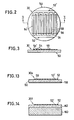
- FIG. 12 is shown a slight modification of the dual collector storage target 30 of FIGS. 2 and 3.
- the modified storage target 30d has two collector electrodes 52a and 52'a which are both of ladderlike shape.
- the first collector electrode 52a underlies the second 52'a.
- a pair of insulating bands 156 electrically insulate the two collector electrodes from each other.
- the strips 54 and 54' of the collector electrodes are arranged alternately in parallel spaced relation to one another, so that this storage target 30d is essentially equivalent to the FIGS. 2 and 3 storage target 30.
- FIG. 12 it is apparent that the principles of FIG. 12 are applicable to the triple collector storage targets in accordance with the invention.
- the collector electrodes could be of ladderlike shape.
- FIG. 13 also shows a slight modification of the FIGS. 2 and 3 dual collector storage target 30.
- the modified storage target 30e features a backing electrode 158, itself conventional, on the surface of the monocrystalline sapphire substrate 50 opposite to its storage surface 58 bearing the two collector electrodes 52 and 52'.
- a required voltage is to be applied to the backing electrode 158 in the operation of the storage tube incorporating this target.
- a similar electrode may of course be provided in cases where the substrate has three or more collector electrodes on its storage surface.
- the monocrystalline sapphire substrate 50 is not an essential feature of this invention.
- the monocrystalline sapphire substrate is replaced by a combination of a monocrystalline silicon layer 160 and a polycrystalline silicon dioxide storage layer 162.
- Collector electrodes, such as those designated 52 and 52', are formed on the storage layer 162.
- FIG. 15 is an illustration of a modified storage tube 20b, differing from the storage tubes 20 and 20a only in having no field mesh electrode.
- the storage target 30 is shown incorporated in this modified storage tube 20b by way of example.
- the omission of the field mesh electrode not only presents no impediment to the writing and reading of information in accordance with the teachings of the instant invention but also offers some positive advantages.
- One of these is that since the beam of primary electrons is not to be caught by the field mesh electrode, the electron beam more efficiently impinges on the target to assure a higher writing speed.
- Another is an increase in resolution through the elimination of "writing" by secondary electrons from the field mesh electrode.
- the wall electrode 46 may affect the storage target 30 the same way as would the field mesh electrode. Desirably, therefore, the potentials of the collector electrodes 52 and 52' of the target 30 may be set higher than that of the wall electrode 46.
- FIG. 16 represents modified means for the application of voltages to the collector electrodes 52 and 52' of the storage target 30 in the storage tube 20 of FIG. 4, in the practice of the second described method of its operation.
- the first collector electrode 52 is coupled to a single power supply 164 via the resistor 66 whereas the second collector electrode 52' can be selectively coupled, via the switch 86, to the power supply 94 and to the first recited power supply 164.
- the power supplies 94 and 164 are voltage sources capable of delivering voltages with a difference of, say, 100 V. In the prime (preerase) and read modes the same voltage may be applied from the power supply 164 to both collector electrodes 52 and 52'. In the write mode, different voltages may be applied to the collector electrodes from the respective power supplies 94 and 164.
Landscapes
- Image-Pickup Tubes, Image-Amplification Tubes, And Storage Tubes (AREA)
Claims (25)
Applications Claiming Priority (6)
| Application Number | Priority Date | Filing Date | Title |
|---|---|---|---|
| JP21237782A JPS59103254A (ja) | 1982-12-03 | 1982-12-03 | 走査変換型蓄積管の動作方法 |
| JP212377/82 | 1982-12-03 | ||
| JP212376/82 | 1982-12-03 | ||
| JP21237682A JPS59103253A (ja) | 1982-12-03 | 1982-12-03 | 走査変換型蓄積管の動作方法 |
| JP21237582A JPS59103249A (ja) | 1982-12-03 | 1982-12-03 | 走査変換型蓄積管 |
| JP212375/82 | 1982-12-03 |
Publications (2)
| Publication Number | Publication Date |
|---|---|
| EP0111201A1 EP0111201A1 (fr) | 1984-06-20 |
| EP0111201B1 true EP0111201B1 (fr) | 1987-03-04 |
Family
ID=27329356
Family Applications (1)
| Application Number | Title | Priority Date | Filing Date |
|---|---|---|---|
| EP83111624A Expired EP0111201B1 (fr) | 1982-12-03 | 1983-11-21 | Tube à mémoire à balayage à cible à collecteur multiple et méthode de fonctionnement |
Country Status (3)
| Country | Link |
|---|---|
| US (1) | US4599541A (fr) |
| EP (1) | EP0111201B1 (fr) |
| DE (1) | DE3370097D1 (fr) |
Families Citing this family (1)
| Publication number | Priority date | Publication date | Assignee | Title |
|---|---|---|---|---|
| FR2595162B1 (fr) * | 1986-02-28 | 1988-05-06 | Labo Electronique Physique | Dispositif d'enregistrement et de restitution de signaux electriques muni d'un predeclenchement, comprenant un dispositif a transfert de charges et oscilloscope utilisant un tel dispositif |
Family Cites Families (9)
| Publication number | Priority date | Publication date | Assignee | Title |
|---|---|---|---|---|
| US2618762A (en) * | 1945-04-12 | 1952-11-18 | Rca Corp | Target and circuit for storage tubes |
| DE1114948B (de) * | 1956-09-04 | 1961-10-12 | Albiswerke Zuerich A G | Speicherelektrode fuer Kathodenstrahl-speicherroehren |
| US3626388A (en) * | 1968-04-24 | 1971-12-07 | Matsushita Electric Industrial Co Ltd | Storage device having an alkali-halide storage surface |
| US3719778A (en) * | 1971-03-02 | 1973-03-06 | Westinghouse Electric Corp | Multielectrode signal plate storage tube for standards conversion of electrical signals |
| JPS5141536B2 (fr) * | 1972-01-31 | 1976-11-10 | ||
| US3873873A (en) * | 1973-05-29 | 1975-03-25 | Rca Corp | Digital storage tube target structure |
| JPS5418160U (fr) * | 1977-04-14 | 1979-02-06 | ||
| JPS5939857B2 (ja) * | 1978-10-09 | 1984-09-26 | 岩崎通信機株式会社 | 走査変換型蓄積管の動作方法 |
| JPS59103248A (ja) * | 1982-12-03 | 1984-06-14 | Iwatsu Electric Co Ltd | 蓄積タ−ゲツトの製造方法 |
-
1983
- 1983-11-18 US US06/553,301 patent/US4599541A/en not_active Expired - Fee Related
- 1983-11-21 DE DE8383111624T patent/DE3370097D1/de not_active Expired
- 1983-11-21 EP EP83111624A patent/EP0111201B1/fr not_active Expired
Also Published As
| Publication number | Publication date |
|---|---|
| DE3370097D1 (en) | 1987-04-09 |
| US4599541A (en) | 1986-07-08 |
| EP0111201A1 (fr) | 1984-06-20 |
Similar Documents
| Publication | Publication Date | Title |
|---|---|---|
| US3710173A (en) | Direct viewing storage tube having mesh halftone target and nonmesh bistable target | |
| US3531675A (en) | Cathode ray storage tube having a target dielectric with collector electrodes extending therethrough | |
| US2877376A (en) | Phosphor screen device | |
| US2259506A (en) | Cathode ray tube oscillograph | |
| US3447043A (en) | Tunnel cathode in matrix form with integral storage feature | |
| EP0111201B1 (fr) | Tube à mémoire à balayage à cible à collecteur multiple et méthode de fonctionnement | |
| US2788466A (en) | Direct-viewing storage tube | |
| US2726328A (en) | Binary storage system | |
| US3356878A (en) | Signal converting cathode ray tube with controllable erasure | |
| US4005408A (en) | Multiple electron beam analog to digital converter | |
| CA1126866A (fr) | Convertisseur de balayage d'ecran cathodique a plaque multiplicatrice de canal et methode de conversion de balayage | |
| US3675134A (en) | Method of operating an information storage tube | |
| US4139800A (en) | Bistable storage target having interdigitated target electrode for selective erasure | |
| US3687665A (en) | Method of manufacturing cathode ray storage tube target | |
| US3611000A (en) | Selective erasure of a bistable storage tube | |
| US3541384A (en) | Image storage apparatus | |
| US3278780A (en) | Storage display tube with a shield separator between the writing gun and the flood gun | |
| US3493803A (en) | Dielectric coated mesh storage target having conductive regions co-terminous with the mesh for use in scan converter tubes | |
| US4288720A (en) | Method of erasing information in a scan converter storage tube | |
| US3940651A (en) | Target structure for electronic storage tubes of the coplanar grid type having a grid structure of at least one pedestal mounted layer | |
| EP0110283B1 (fr) | Cible accumulatrice pour tubes à mémoire et procédé de fabrication de ladite cible | |
| US3982191A (en) | Charge storage tube and method for operating the same | |
| US3175114A (en) | Storage cathode ray tubes | |
| US2704328A (en) | Electron-beam tube oscillator | |
| US3579013A (en) | Cathode ray tube having radially directed commutator elements |
Legal Events
| Date | Code | Title | Description |
|---|---|---|---|
| PUAI | Public reference made under article 153(3) epc to a published international application that has entered the european phase |
Free format text: ORIGINAL CODE: 0009012 |
|
| AK | Designated contracting states |
Designated state(s): DE FR NL |
|
| 17P | Request for examination filed |
Effective date: 19840913 |
|
| GRAA | (expected) grant |
Free format text: ORIGINAL CODE: 0009210 |
|
| AK | Designated contracting states |
Kind code of ref document: B1 Designated state(s): DE FR NL |
|
| REF | Corresponds to: |
Ref document number: 3370097 Country of ref document: DE Date of ref document: 19870409 |
|
| R20 | Corrections of a patent specification |
Effective date: 19870302 |
|
| ET | Fr: translation filed | ||
| PLBE | No opposition filed within time limit |
Free format text: ORIGINAL CODE: 0009261 |
|
| STAA | Information on the status of an ep patent application or granted ep patent |
Free format text: STATUS: NO OPPOSITION FILED WITHIN TIME LIMIT |
|
| 26N | No opposition filed | ||
| PGFP | Annual fee paid to national office [announced via postgrant information from national office to epo] |
Ref country code: FR Payment date: 19911018 Year of fee payment: 9 |
|
| PGFP | Annual fee paid to national office [announced via postgrant information from national office to epo] |
Ref country code: NL Payment date: 19911130 Year of fee payment: 9 |
|
| PGFP | Annual fee paid to national office [announced via postgrant information from national office to epo] |
Ref country code: DE Payment date: 19920131 Year of fee payment: 9 |
|
| PG25 | Lapsed in a contracting state [announced via postgrant information from national office to epo] |
Ref country code: NL Effective date: 19930601 |
|
| NLV4 | Nl: lapsed or anulled due to non-payment of the annual fee | ||
| PG25 | Lapsed in a contracting state [announced via postgrant information from national office to epo] |
Ref country code: FR Effective date: 19930730 |
|
| PG25 | Lapsed in a contracting state [announced via postgrant information from national office to epo] |
Ref country code: DE Effective date: 19930803 |
|
| REG | Reference to a national code |
Ref country code: FR Ref legal event code: ST |