EP0111741A2 - Circuit semi-conducteur intégré avec une mémoire dynamique lecture-écriture - Google Patents
Circuit semi-conducteur intégré avec une mémoire dynamique lecture-écriture Download PDFInfo
- Publication number
- EP0111741A2 EP0111741A2 EP83111294A EP83111294A EP0111741A2 EP 0111741 A2 EP0111741 A2 EP 0111741A2 EP 83111294 A EP83111294 A EP 83111294A EP 83111294 A EP83111294 A EP 83111294A EP 0111741 A2 EP0111741 A2 EP 0111741A2
- Authority
- EP
- European Patent Office
- Prior art keywords
- output
- clock
- gate
- cas
- address clock
- Prior art date
- Legal status (The legal status is an assumption and is not a legal conclusion. Google has not performed a legal analysis and makes no representation as to the accuracy of the status listed.)
- Granted
Links
- 230000015654 memory Effects 0.000 title claims abstract description 60
- 239000004065 semiconductor Substances 0.000 title claims description 24
- 239000011159 matrix material Substances 0.000 claims abstract description 17
- 230000005540 biological transmission Effects 0.000 claims abstract description 3
- 238000000034 method Methods 0.000 claims abstract description 3
- 238000013500 data storage Methods 0.000 claims abstract 3
- 230000005669 field effect Effects 0.000 claims description 25
- 238000012546 transfer Methods 0.000 claims description 14
- 230000000694 effects Effects 0.000 claims description 6
- 230000000717 retained effect Effects 0.000 claims description 3
- 239000012071 phase Substances 0.000 claims 2
- 239000012072 active phase Substances 0.000 claims 1
- 230000003750 conditioning effect Effects 0.000 claims 1
- 230000001404 mediated effect Effects 0.000 claims 1
- 238000010586 diagram Methods 0.000 description 7
- 238000013461 design Methods 0.000 description 6
- 230000006399 behavior Effects 0.000 description 3
- 239000003990 capacitor Substances 0.000 description 3
- 230000006870 function Effects 0.000 description 2
- 230000004913 activation Effects 0.000 description 1
- 238000011157 data evaluation Methods 0.000 description 1
- 230000003111 delayed effect Effects 0.000 description 1
- 230000009977 dual effect Effects 0.000 description 1
- 238000011835 investigation Methods 0.000 description 1
- 239000013589 supplement Substances 0.000 description 1
- 230000001360 synchronised effect Effects 0.000 description 1
- 230000001550 time effect Effects 0.000 description 1
- 230000007704 transition Effects 0.000 description 1
Images


Classifications
-
- G—PHYSICS
- G11—INFORMATION STORAGE
- G11C—STATIC STORES
- G11C7/00—Arrangements for writing information into, or reading information out from, a digital store
- G11C7/10—Input/output [I/O] data interface arrangements, e.g. I/O data control circuits, I/O data buffers
- G11C7/1015—Read-write modes for single port memories, i.e. having either a random port or a serial port
- G11C7/1018—Serial bit line access mode, e.g. using bit line address shift registers, bit line address counters, bit line burst counters
- G11C7/1021—Page serial bit line access mode, i.e. using an enabled row address stroke pulse with its associated word line address and a sequence of enabled column address stroke pulses each with its associated bit line address
- G11C7/1024—Extended data output [EDO] mode, i.e. keeping output buffer enabled during an extended period of time
-
- G—PHYSICS
- G11—INFORMATION STORAGE
- G11C—STATIC STORES
- G11C11/00—Digital stores characterised by the use of particular electric or magnetic storage elements; Storage elements therefor
- G11C11/21—Digital stores characterised by the use of particular electric or magnetic storage elements; Storage elements therefor using electric elements
- G11C11/34—Digital stores characterised by the use of particular electric or magnetic storage elements; Storage elements therefor using electric elements using semiconductor devices
- G11C11/40—Digital stores characterised by the use of particular electric or magnetic storage elements; Storage elements therefor using electric elements using semiconductor devices using transistors
- G11C11/401—Digital stores characterised by the use of particular electric or magnetic storage elements; Storage elements therefor using electric elements using semiconductor devices using transistors forming cells needing refreshing or charge regeneration, i.e. dynamic cells
- G11C11/4063—Auxiliary circuits, e.g. for addressing, decoding, driving, writing, sensing or timing
- G11C11/407—Auxiliary circuits, e.g. for addressing, decoding, driving, writing, sensing or timing for memory cells of the field-effect type
- G11C11/409—Read-write [R-W] circuits
- G11C11/4093—Input/output [I/O] data interface arrangements, e.g. data buffers
-
- G—PHYSICS
- G11—INFORMATION STORAGE
- G11C—STATIC STORES
- G11C11/00—Digital stores characterised by the use of particular electric or magnetic storage elements; Storage elements therefor
- G11C11/21—Digital stores characterised by the use of particular electric or magnetic storage elements; Storage elements therefor using electric elements
- G11C11/34—Digital stores characterised by the use of particular electric or magnetic storage elements; Storage elements therefor using electric elements using semiconductor devices
- G11C11/40—Digital stores characterised by the use of particular electric or magnetic storage elements; Storage elements therefor using electric elements using semiconductor devices using transistors
- G11C11/401—Digital stores characterised by the use of particular electric or magnetic storage elements; Storage elements therefor using electric elements using semiconductor devices using transistors forming cells needing refreshing or charge regeneration, i.e. dynamic cells
- G11C11/4063—Auxiliary circuits, e.g. for addressing, decoding, driving, writing, sensing or timing
- G11C11/407—Auxiliary circuits, e.g. for addressing, decoding, driving, writing, sensing or timing for memory cells of the field-effect type
- G11C11/409—Read-write [R-W] circuits
- G11C11/4096—Input/output [I/O] data management or control circuits, e.g. reading or writing circuits, I/O drivers or bit-line switches
-
- G—PHYSICS
- G11—INFORMATION STORAGE
- G11C—STATIC STORES
- G11C7/00—Arrangements for writing information into, or reading information out from, a digital store
- G11C7/10—Input/output [I/O] data interface arrangements, e.g. I/O data control circuits, I/O data buffers
- G11C7/1015—Read-write modes for single port memories, i.e. having either a random port or a serial port
- G11C7/103—Read-write modes for single port memories, i.e. having either a random port or a serial port using serially addressed read-write data registers
- G11C7/1033—Read-write modes for single port memories, i.e. having either a random port or a serial port using serially addressed read-write data registers using data registers of which only one stage is addressed for sequentially outputting data from a predetermined number of stages, e.g. nibble read-write mode
-
- G—PHYSICS
- G11—INFORMATION STORAGE
- G11C—STATIC STORES
- G11C8/00—Arrangements for selecting an address in a digital store
- G11C8/04—Arrangements for selecting an address in a digital store using a sequential addressing device, e.g. shift register, counter
Definitions
- the present invention relates to an integrated semiconductor circuit with a dynamic read / write memory, in which the memory matrix constructed from the same memory cells, in particular one-transistor memory cells, can be addressed with respect to the individual memory cells via row and column decoders, and the addressing according to single matrix row address strobe-initiated column is connected by a line address strobe and the addressing according to the individual matrix columns by one, and in which, finally, the addressing is designed such that during read-out operation at the same time the information of at least two of the data records p egg insurance
- the memory cells provided are processed and temporarily stored in an intermediate register, and also a shift register operated exclusively by the column address clock for the serial transmission of the information obtained simultaneously from the memory matrix to the data output of the memory rs is provided.
- RAS row address strobe
- RAS decoding is also controlled by the column address clock CAS. It activates the sense amplifier associated with the addressed column line, which - as already indicated - acts as a buffer, and switches the connection of the buffer connected to the addressed memory cell to an intermediate register, which at the same time serves to amplify the data again.
- BYTE mode in which an eight-bit data word is made available for each addressing.
- it is the “dual mode”, in which two bits are supplied with each addressing.
- the data stored in the intermediate register are made available in series using the shift register mentioned at the data output of the memory.
- the nibble mode is activated in the DRAM memories designed in this regard in that the row address clock RAS is low and the column address clock CAS is switched to high, whereby the data output is blocked and the column address clock CAS is then set to low again. This will then request the next data bit.
- this operation can be repeated every 55 nsec or 65 nsec, so that a maximum data rate of 14 ... 16 MHz can be expected with a suitably designed control circuit.
- By clocking the voltage on CAS - Connection allows access to four consecutive bits in nibble mode operation. Then the row address clock RAS can be switched to high to start a new access cycle. Four cells are read out again by creating the row and column addresses. This means that random data access remains possible.
- One of the main advantages of operating in nibble mode is faster readout compared to the usual serial operation, ie page mode operation.
- the invention is based on the knowledge that a targeted extension of the storage time of the data output only for nibble mode or byte mode operation, that is, the time period t NOFF ' and by specifying a minimum value t NOFF min for this period of time offers the user the possibility of evaluating the output data, although the period of time t NAS is minimal. However, this also allows the effective minimum cycle time t NC to be further reduced with the nibble mode.
- the control of the data output via the column address clock CAS is designed such that the data output which is pending at the data output and is shifted by the shift register Information provided after the column address clock signal causing its readout has decayed CAS a defined period of time at the data output of the memory, which may extend to the onset of the next column address clock signal CAS, is retained.
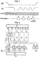
- FIGS. 1 and 2 relate to the prior art, while the other figures refer to ver deal with various embodiments of the invention. First of all, reference is made to the prior art shown in FIGS. 1 and 2.
- FIG. 1 shows the time diagram customary in nibble mode and FIG. 2 shows the simplified block diagram for the DRAM memory customary for this.
- Two associated data outputs O x , O x of the memory matrix SP serve to apply one each of four circuit parts I, II, III and IV, which are identical to one another, so that in the drawing only one of these circuit parts, namely circuit part I, indicates the essential components for nibble mode are.
- These consist of an intermediate register Rg with two signal inputs, each of which contains two outputs O x , O x are controlled.
- the application of one current-carrying connection to one n-channel MOS field-effect transistor t is given second current-carrying connection to one of the two inputs D and D of the common output driver stage OLB.
- one input D with the data obtained on the basis of the addressing and actually stored in the addressed cells, and the other input D charged with the inverted data.
- the data D correspond to the data supplied by the outputs O o , 0 1 , 0 2 and 0 3 of the memory matrix SP, while the data D of the inverted outputs O o , O 1 , U 2 and O 3 of the memory matrix SP.
- the data-carrying output of the individual register stages S1-S4 is used to control the gates of the transistor pair t provided in each of the aforementioned circuit parts I-IV and thus to control the data flow to the output driver OLB.
- the latter also contains the function of level adjustment, e.g. for the operation of a TTL logic.
- the data output DA is given by the output of the circuit part OLB.
- a first embodiment in this regard is described with reference to FIGS. 3, 3a, 3b and 3c.
- one first has one through the two data inputs D and D controlled output register OL ( output latch), which is controlled by a clock ⁇ o .
- D and D controlled output register OL output latch
- a flip-flop clocked by the clock ⁇ o in particular a D-latch, can be used for this purpose.
- the data signal Do to be evaluated and the output of the output register OL carrying the inverted signal Do each serve to control the gate of the two MOS field effect transistors T1 and T2, which are connected in series with one another.
- the one current-carrying connection of this series circuit is connected to the supply potential V CC and is given by the drain of the MOS field-effect transistor T1 controlled by the output Do of the output register OL which carries the data signal to be evaluated.
- the second current-carrying connection of this series circuit is provided by the source connection of the MOS field-effect transistor T2 controlled by the output Do of the output register OL which carries the inverted data signal and is connected to the reference potential V SS .
- the data output DA of the memory is located between the two transistors T1 and T2 of the series circuit mentioned.
- Two further MOS field effect transistors T3 and T4 are used to discharge one of the two data outputs Do and do of the output register OL and thus the gate of the data output Do or do controlled output transistor T1 or T2.
- the output is Do. via the source-drain path of the discharge transistor T3 and the output do connected to the reference potential V SS via the source-drain path of the discharge transistor T4.
- Their gates are ⁇ by a common clock controlled by that of one in turn through the column address clock CAS controlled circuit arrangement is supplied.
- This consists of a circuit part EG, which is acted upon by the column address clock CAS and in turn emits a clock pulse ⁇ k to a delay element VG.
- the clock pulse ⁇ required for controlling the two discharge transistors T3 and T4 then appears at the output of this delay element VG . It has now been shown that the effect sought by the invention comes about precisely through the use of the delay element VG, while in the absence of this delay element VG the pulses ⁇ k supplied by the circuit part EG, the so-called discharge generator, if they are immediate for the Control of the two discharge transistors T3 and T4 would be used, only to those with the previously. applied nibble mode control would result in time effects. However, the invention can also be applied to another. Realize as by a delay element VG.
- the two output transistors T1 and T2 and the two discharge transistors T3 and T4 are normally-off transistors of the same channel type, in particular of the n-channel type, which is generally also the case for the other parts of the memory and that provided in FIG Circuit parts apply.
- the two output transistors T1 and T2 together with the circuit node between them and forming the output DA, form an output buffer operating in tri-state operation.
- the clock pulse ⁇ o controlling the output register OL
- the data coming from the memory matrix SP reach the output buffer T1, T2.
- the clock ⁇ By the clock ⁇ . the outputs Do and do of the exit Registers OL and thus the gate of the output transistors T1 and T2 are pulled to low, that is to say to the reference potential V SS , as a result of which the data output DA enters the tri-state state.
- the associated time diagram can be seen in FIG. 3 a.
- the delay element VG is preferably set to a delay time of 15 nsec and consists, for example, of an even number of inverters connected in series, which are constructed, for example, using n-channel MOS-FETs with normally-off driver transistors. They each consist, for example, of a driver transistor with its source at the reference potential V SS and with its gate forming the inverter input, the drain connection of which forms the signal output of the inverter and which is connected to the supply potential V DD or V CC via a load transistor. If the load transistor is of the same type as the driver transistor, its gate is connected to its drain. If, however, the load transistor is of the self-conducting type, its gate is preferably at the output of the relevant inverter.
- FIG. 3b With regard to a possible configuration of the output register OL and that of the column address clock CAS directly controlled circuit part EG for generating the clock ⁇ k to be applied to the delay element VG can be referred to FIG. 3b. which is otherwise configured with regard to the generation of the pulses ⁇ ' k , which together control the discharge transistors T3 and R4, compared to the system shown in FIG.
- the output register OL consists of a flip-flop which is formed from the cross-coupled MOS field-effect transistors 3 and 4 and the two load transistors 1 and 2.
- the source connections of the two are cross-headed pelten MOS-FET's 3 and 4 at the reference potential V SS and the drain of transistor 3 and the gate of transistor 4 at the source of load transistor 1, while the drain of transistor 4 and the gate of transistor 3 are directly connected to the source of load transistor 2 is.
- the drain connections of the two load transistors are from the mentioned clock signal ⁇ o and the gate of the first load transistor 1 through the data input D and the gate of the second load transistor 2 through the inverted data input D acted upon.
- the circuit node between the transistor 3 and the first load transistor 1 forms the output Do for the non-inverted data signal and the node between the transistor 4 and the second load transistor 2 forms the output Do for the inverted data signal.
- the configuration for the output register OL shown in FIG. 3b can be used both in the configuration in accordance with FIG. 3 and in the configuration in accordance with FIG.
- the transistors in the output register OL are also normally-off transistors of the same channel conductivity type as the transistors T1-T4.
- the generation of the circuit part EG provided for the control of the delay element VG is provided, for example, by a MOS amplifier of a known type, the input of which is provided by the column address clock signal CAS is applied and the output of which supplies the clock signal ⁇ k , which is provided to act on the delay element VG.
- the delay element VG consists in the drawn case Game case from two series-connected MOS inverters of conventional design ..
- the output of the second inverter is connected directly to the one input of an AND gate U1, while the second input of this AND gate U1 is directly connected to the output of the circuit part EG, that is the pulses ⁇ k is controlled.
- the pulses ⁇ ' k appear , which are used to control the discharge of the two data outputs Do and Do and the gate of the two output transistors T1 and T2 by means of transistors T3 and T4.
- FIG. 3c With regard to a possibility of generating the clock pulses ⁇ o required for controlling the output register OL, reference is made to FIG. 3c.
- the output of this NOR gateps N1 controls the set input of a flip-flop FF, for example an RS flip-flop, whose reset input is from the row address clock signals RAS is acted upon.
- the output Q of the flip-flop FF which supplies the non-inverted signal, is connected to the one input of an AND gate U2 via a delay element T1I2.
- the second input of this AND gate U2 is controlled by the output of an inverter 13, the input of which is controlled by the column Address clock signal CAS is immediately applied.
- the signal output of the AND gate U2 supplies the desired clock pulses ⁇ o , which are used for the clock control of the output register OL, for example in the manner shown in FIG. 3b. However, they are also used in the same way as in FIG. 3b to control the configuration for the output register OL used in the configuration according to FIGS. 5, 5a, 5b, as can be seen from FIG. 5b.
- the circuit shown in Figure 3c for generating the clock pulses ⁇ o causes - after the row address clock CAS has gone LOW - the first ⁇ o pulse with a time delay compared to the column address clock CAS goes to HIGH. During this time, the data are read from the memory cells in the matrix SP and stored in the intermediate register Rg (see FIG. 2). The following ⁇ o pulses have only a slight delay compared to CAS.
- a specific extension of the storage time of the data output DA (that is to say of the two output transistors T1 and T2) is to be achieved, specifically restricted to the case that the memory circuit is operated in nibble mode or in byte mode.
- This means that such an extension of the storage time is only given if the column address is switched off when the data output DA is switched off CAS the row address bar RAS is at the LOW level, as can be seen in detail from the time diagram according to FIG. 4b.
- the previously short storage time for normal operation with the line address clock should be RAS be maintained at the HIGH level.
- t NOFF is the period of time that elapses until the data output DA is switched off and begins with the transition of the column address clock signal from LOW to HIGH, the row address clock RAS likewise having the LOW state. If, on the other hand, the row address clock RAS is HIGH when the data output DA is switched off, the delay specified above does not take effect. The time period corresponding to it is designated in FIG. 4b by "t OFF ".
- the circuit for the output driver OLB shown in FIG. 4 differs from the circuit according to FIGS. 3 and 3b only by a different structure of the part of the output circuit OLB which serves to generate the clock ⁇ ' k which controls the gates of the two discharge transistors T3 and T4.
- the output of the pulses ⁇ k which is effective as a discharge generator and in turn controlled by the column address clock CAS, is connected to a circuit node K via the series connection of the delay element VG and the source-drain path of a transfer transistor.
- the same output of the discharge generator EG is also applied to said node K via a second transfer transistor T6.
- Controlled circuit TG which two inverted clock signals ⁇ R and O R delivers.
- the one clock signal ⁇ R serves to control the transistor T5 and thus the connection between the output of the delay element VG and said node K.
- the other - inverted to the first clock signal ⁇ R - clock signal O R is used to control the transfer transistor T6 and thus to control the direct connection between the output of the discharge generator EG and said node K.
- This superimposition creates the pulses used to control the gate of the two discharge transistors T3, T4.
- the timing of the impulses ⁇ R and O R in relation to the other impulses, especially the impulses RAS and CAS can be seen from the time diagram according to FIG. 4b.
- FIG. 4a A simple method for generating the pulses ⁇ R and required for clocking the two transfer transistors T5 and T6 O R is shown in Figure 4a. This is used to generate the pulses required for controlling the transfer transistor T6 forming the connection between the node K and the output of the discharge generator EG O R the line address clock RAS via a non-inverting MOS amplifier V to the gate of transistor T6.
- a clock ⁇ R is used to control the gate of the transfer transistor forming the connection between the output of the delay element VG and the node K, which is caused by the application of an inverter 13 by the row address clock RAS arises.
- the amplifier V can be given, for example (corresponding to the delay element VG according to FIG.
- FIG. 4c the circuit for the inverter 13 provided in the embodiment according to FIG. 4a and FIG. 4d represents the circuit for the amplifier V.
- D a it is in the illustrated in Figure 4c and 4d circuits to a per se conventional ways to implement an inverting amplifier and a non-inverting amplifier in MOS technology with the same delay time and also the desired effect will be readily apparent, can range from a detailed description of of Figures 4c and 4d.
- the transistors b, d, f, h, k, m with their drain at the supply potential are of the depletion type and the other transistors a, c, e, g, i, 1 are of the enhancement type.
- the first two stages a, b, c, d and g, h, i, k each form an amplifier, while the output stages f, e and m, 1 of the first two stages are shown in FIGS. 4c and 4d Controlled way.
- the design shown in FIG. 5 for the output OLB of a DRAM memory according to the invention is designed in such a way that the following behavior is ensured:
- both the row address clock RAS and the column address clock are used in the data output circuit shown in FIG. 5 according to the invention CAS used both for the common control of an AND gate U3 and for the common control of a NOR gate N2.
- FIG. 5e The decisive time diagram for the circuit according to FIG. 5 is shown in FIG. 5e.
- the circuit already presented with reference to FIG. 3c can be used to generate the clock pulses 0, while one can generate ⁇ c and O c can proceed according to FIG. 5c.
- one has an inverter I4 for generating the clock ⁇ c the input of which is acted upon by the column address clock CAS.
- To generate the inverted clock you have one on its input side with the column address clock CAS acted upon amplifier V *.
- the MOS circuit shown in FIG. 4c and the amplifier V * in FIG. 4d can be used for the inverter I4.
- the circuit shown in FIG. 5 can now be further developed with regard to the system used to generate the discharge clock ⁇ M by using the row address clock RAS via a delay element VZ to the AND gate U3, while - as shown in FIG. 5a - the circuit used in FIG. 5 to apply the RS flip-flop FFL is otherwise unchanged.
- This delay element VZ can in turn be provided by two inverters connected in series. The delay element VZ leads, as can be readily seen, to the fact that the data address pending at the data output DA is switched off by the row address RAS experiences a further delay.
- FIG. 5'b shows the circuit for the output register OL *, as is required in connection with FIG. 5.
- the core here is also the flip-flop oL consisting of transistors 1-4 according to FIG. 3b for the output register OIL.
- MOS field effect transistors 5-10 of the same type as the transistors 1-4 and T1-T4 (ie of the enhancement type with matching channel doping) are provided.
- the data input D is connected to the gate of the transistor 1 of the flip-flop via a transfer transistor 5 controlled by the clock ⁇ C and also to the reference potential V SS via two MOS-FETs 7 and 9 connected in parallel .
- the data input D to which the inverted data signal is applied is connected to the gate of the transistor 2 of the flip-flop via a transfer transistor 6, which is also controlled by the clock ⁇ C , and is also connected to the reference potential by the parallel connection of the two MOS-FETs 8 and 10 V SS connected.
- one transistor in the example the transistor 7 and 10) is by the inverted clock signal O C controlled.
- the gate of the respective other MOS field-effect transistor of the said parallel circuit is with that data output do or Do of the output register OL connected to that of the two data inputs D or D ge3aört, which is connected to the reference potential via the series circuit of its input transistor 5 or 2 with the relevant transistor parallel circuit 7,9 or 8, 10 respectively.
- FIG. 5d a one-channel MOS circuit is shown for generating the Entladetakts ⁇ M corresponding to ⁇ in principle indicated in Figure 5 circuit for generating the clock M.
- the circuit shown in FIG. 5d for generating the clock ⁇ M consists of the transistors 11-29 and 5 capacitors C1-C5.
- the transistors are of the same channel type as the other transistors used in the circuit and are preferably self-blocking.
- the row address clock controls RAS the first transistor 13 of this circuit, which is connected to the supply potential V CC with its source at the reference potential V SS and with its drain via a bootstrap load formed by the two MOS field-effect transistors 11 and 12 and the capacitor C1. This creates an inverter effect, but the output signal has a high output level which is equal to the supply voltage.
- a second boat zap inverter stage is constructed in the same way as the first bootstrap stage. controlled at the gate of its driver transistor 16 by the output A of the first inverter stage.
- the bootstrap load constructed from the two transistors 14 and 15 and the capacitor C2 corresponds to the first bootstrap converter stage, just like the rest of the circuit.
- a third bootstrap converter has a drive transistor 19 which is driven by the column address clock CAS is controlled.
- the bootstraplast of this inverter is precharged via the MOS field-effect transistor 17 forming part of this load via its drain from the output A of the first bootstrap converter stage in the manner shown in FIG. 5d. Otherwise, the structure of the load element of the third inverter stage corresponds to the structure of the load for the other inverter stages of this circuit.
- a fourth bootstrap printer is controlled at its driver transistor 22 by the output of the third inverter stage 19, 17, 18.
- the first, the second and the fourth bootstrap converter circuit are identical, while the third inverter stage deviates slightly with regard to the control of the load by the output A of the first inverter, as can be seen from FIG. 5d.
- An inverter stage constructed from the driver transistor 29 and the bootstraplast 27, 28 and C5 forms the signal output of the circuit.
- the desired signal ⁇ M can be taken off at the drain of the driver transistor 29 of this fifth inverter stage.
- the fifth inverter stage is controlled on its driver transistor by a pre-stage formed by transistors 23-26, which in turn is controlled on the one hand by the output of the second inverter stage, i.e. output B, on the other hand by the output of the third and fourth inverter stage and finally by the signal output the fifth inverter stage is fed back.
- the transistor having its D rain to the supply potential V CC lying 23 of this intermediate by the output of the third inverter stage, so the drain of the by CAS controlled driver transistor 19, controlled by its gate connected to this output.
- the source of the transistor 23 of the intermediate stage is the drain of a transistor 26, the source of which is at the reference potential V SS and the gate of which is at the drain of the driver transistor 29 of the last inverter stage.
- the source of the transistor 23 of the intermediate stage is connected to the reference potential via the series connection of two further transistors 24 and 25, the transistor 25 lying directly at the reference potential being connected to the output of the fourth inverter stage, that is to say the drain of the driver transistor 22, and the one directly at the Source of transistor 23, transistor 24 is controlled at its gate by the output of the second inverter stage, that is to say the drain of transistor 16.
- the described exemplary embodiments of the invention have the property of being able to be represented with little effort with regard to the timing.
Landscapes
- Engineering & Computer Science (AREA)
- Microelectronics & Electronic Packaging (AREA)
- Computer Hardware Design (AREA)
- Databases & Information Systems (AREA)
- Dram (AREA)
- Semiconductor Memories (AREA)
- Static Random-Access Memory (AREA)
Priority Applications (1)
| Application Number | Priority Date | Filing Date | Title |
|---|---|---|---|
| AT83111294T ATE35477T1 (de) | 1982-11-24 | 1983-11-11 | Integrierte halbleiterschaltung mit einem dynamischen schreib-lese-speicher. |
Applications Claiming Priority (2)
| Application Number | Priority Date | Filing Date | Title |
|---|---|---|---|
| DE3243496 | 1982-11-24 | ||
| DE19823243496 DE3243496A1 (de) | 1982-11-24 | 1982-11-24 | Integrierte halbleiterschaltung mit einem dynamischen schreib-lese-speicher |
Publications (3)
| Publication Number | Publication Date |
|---|---|
| EP0111741A2 true EP0111741A2 (fr) | 1984-06-27 |
| EP0111741A3 EP0111741A3 (en) | 1985-05-22 |
| EP0111741B1 EP0111741B1 (fr) | 1988-06-29 |
Family
ID=6178931
Family Applications (1)
| Application Number | Title | Priority Date | Filing Date |
|---|---|---|---|
| EP83111294A Expired EP0111741B1 (fr) | 1982-11-24 | 1983-11-11 | Circuit semi-conducteur intégré avec une mémoire dynamique lecture-écriture |
Country Status (6)
| Country | Link |
|---|---|
| US (1) | US4602353A (fr) |
| EP (1) | EP0111741B1 (fr) |
| JP (1) | JPS59110094A (fr) |
| AT (1) | ATE35477T1 (fr) |
| DE (2) | DE3243496A1 (fr) |
| HK (1) | HK84692A (fr) |
Cited By (3)
| Publication number | Priority date | Publication date | Assignee | Title |
|---|---|---|---|---|
| EP0125699A3 (fr) * | 1983-05-17 | 1986-10-08 | Kabushiki Kaisha Toshiba | Circuit de sortie de données pour un dispositif de mémoire dynamique |
| EP0182194A3 (en) * | 1984-11-05 | 1987-10-07 | Kabushiki Kaisha Toshiba | Data output circuit for a dynamic memory |
| EP0607668B1 (fr) * | 1993-01-21 | 1999-03-03 | Advanced Micro Devices, Inc. | Système et procédé de mémoire électronique |
Families Citing this family (15)
| Publication number | Priority date | Publication date | Assignee | Title |
|---|---|---|---|---|
| JPS60117492A (ja) * | 1983-11-29 | 1985-06-24 | Fujitsu Ltd | 半導体記憶装置 |
| JPS60136086A (ja) * | 1983-12-23 | 1985-07-19 | Hitachi Ltd | 半導体記憶装置 |
| GB8401804D0 (en) * | 1984-01-24 | 1984-02-29 | Int Computers Ltd | Data storage apparatus |
| JPS6363200A (ja) * | 1986-09-03 | 1988-03-19 | Mitsubishi Electric Corp | 半導体記憶装置 |
| US4792929A (en) * | 1987-03-23 | 1988-12-20 | Zenith Electronics Corporation | Data processing system with extended memory access |
| JPH0752583B2 (ja) * | 1987-11-30 | 1995-06-05 | 株式会社東芝 | 半導体メモリ |
| KR920000962B1 (ko) * | 1989-05-26 | 1992-01-31 | 삼성전자 주식회사 | 반도체 메모리 장치의 데이터 출력단 전압레벨 조절회로 |
| JPH0828820B2 (ja) * | 1990-05-28 | 1996-03-21 | 村田機械株式会社 | 画像データ符号化回路 |
| US5488581A (en) * | 1993-10-28 | 1996-01-30 | Fujitsu Limited | Semiconductor memory device |
| JPH08315567A (ja) * | 1995-05-22 | 1996-11-29 | Mitsubishi Electric Corp | 半導体記憶装置 |
| US6022094A (en) * | 1995-09-27 | 2000-02-08 | Lexmark International, Inc. | Memory expansion circuit for ink jet print head identification circuit |
| US5699530A (en) * | 1995-10-03 | 1997-12-16 | Intel Corporation | Circular RAM-based first-in/first-out buffer employing interleaved storage locations and cross pointers |
| DE10330825A1 (de) * | 2003-07-08 | 2005-06-23 | Infineon Technologies Ag | Integrierter Schaltkreis |
| KR101796116B1 (ko) | 2010-10-20 | 2017-11-10 | 삼성전자 주식회사 | 반도체 장치, 이를 포함하는 메모리 모듈, 메모리 시스템 및 그 동작방법 |
| US9159383B2 (en) | 2012-04-11 | 2015-10-13 | Micron Technology, Inc. | Signal management in a memory device |
Family Cites Families (8)
| Publication number | Priority date | Publication date | Assignee | Title |
|---|---|---|---|---|
| US3969706A (en) * | 1974-10-08 | 1976-07-13 | Mostek Corporation | Dynamic random access memory misfet integrated circuit |
| JPS5521309A (en) * | 1978-07-26 | 1980-02-15 | Unic Corp | Remoteecontrolling apparatus for hydraulic crane |
| JPS55132595A (en) * | 1979-04-04 | 1980-10-15 | Nec Corp | Semiconductor circuit |
| JPS5625290A (en) * | 1979-08-07 | 1981-03-11 | Nec Corp | Semiconductor circuit |
| JPS56101694A (en) * | 1980-01-18 | 1981-08-14 | Nec Corp | Semiconductor circuit |
| JPS5951073B2 (ja) * | 1980-03-27 | 1984-12-12 | 富士通株式会社 | 半導体記憶装置 |
| DE3134065A1 (de) * | 1981-08-28 | 1983-03-10 | Mannesmann Rexroth GmbH, 8770 Lohr | Druckregelventil |
| JPS58222479A (ja) * | 1982-06-18 | 1983-12-24 | Hitachi Ltd | 半導体メモリのデ−タ読み出し方式 |
-
1982
- 1982-11-24 DE DE19823243496 patent/DE3243496A1/de not_active Withdrawn
-
1983
- 1983-11-11 DE DE8383111294T patent/DE3377244D1/de not_active Expired
- 1983-11-11 AT AT83111294T patent/ATE35477T1/de not_active IP Right Cessation
- 1983-11-11 EP EP83111294A patent/EP0111741B1/fr not_active Expired
- 1983-11-21 US US06/554,432 patent/US4602353A/en not_active Expired - Lifetime
- 1983-11-22 JP JP58220479A patent/JPS59110094A/ja active Granted
-
1992
- 1992-10-29 HK HK846/92A patent/HK84692A/xx not_active IP Right Cessation
Cited By (3)
| Publication number | Priority date | Publication date | Assignee | Title |
|---|---|---|---|---|
| EP0125699A3 (fr) * | 1983-05-17 | 1986-10-08 | Kabushiki Kaisha Toshiba | Circuit de sortie de données pour un dispositif de mémoire dynamique |
| EP0182194A3 (en) * | 1984-11-05 | 1987-10-07 | Kabushiki Kaisha Toshiba | Data output circuit for a dynamic memory |
| EP0607668B1 (fr) * | 1993-01-21 | 1999-03-03 | Advanced Micro Devices, Inc. | Système et procédé de mémoire électronique |
Also Published As
| Publication number | Publication date |
|---|---|
| JPH0450679B2 (fr) | 1992-08-14 |
| ATE35477T1 (de) | 1988-07-15 |
| DE3377244D1 (en) | 1988-08-04 |
| US4602353A (en) | 1986-07-22 |
| DE3243496A1 (de) | 1984-05-24 |
| EP0111741A3 (en) | 1985-05-22 |
| HK84692A (en) | 1992-11-06 |
| JPS59110094A (ja) | 1984-06-25 |
| EP0111741B1 (fr) | 1988-06-29 |
Similar Documents
| Publication | Publication Date | Title |
|---|---|---|
| DE3687533T2 (de) | Statische halbleiterspeicheranordnung. | |
| EP0111741B1 (fr) | Circuit semi-conducteur intégré avec une mémoire dynamique lecture-écriture | |
| DE3588247T2 (de) | Dynamischer Halbleiterspeicher mit einer statischen Datenspeicherzelle | |
| DE3685615T2 (de) | Leseverstaerkerschaltung. | |
| DE3884022T2 (de) | Halbleiterspeicheranordnung. | |
| DE2548564A1 (de) | Halbleiterspeicher mit wahlfreiem zugriff | |
| DE2545313A1 (de) | Dynamischer misfet randomspeicher in integrierter schaltung | |
| DE3203825A1 (de) | Signalverarbeitungsschaltung | |
| DE69120447T2 (de) | Halbleiterspeicheranordnung von dynamischem Typus | |
| DE2300186A1 (de) | Mos-pufferschaltung, insbesondere fuer ein mos-speichersystem | |
| DE69221827T2 (de) | Verfahren zum Programmieren einer anwenderprogrammierbaren Gattermatrix | |
| DE3789726T2 (de) | Register mit Einrichtungen zum gleichzeitigen Auslesen und Einschreiben über vielfache Anschlüsse. | |
| DE4004771C2 (fr) | ||
| EP0120458B1 (fr) | Mémoire intégrée de lecture-écriture dynamique | |
| EP0056433A2 (fr) | Circuit de lecture pour une mémoire monolithique intégrée semiconductrice | |
| DE3740314C2 (fr) | ||
| DE4003690C2 (de) | Schaltkreis zum Einstellen eines Spannungspegels entsprechend den Ausgangsdaten eines Halbleiterspeichers | |
| DE3334560A1 (de) | Halbleiterspeicher | |
| DE3786382T2 (de) | Halbleiterspeicheranordnung mit Datenbusrücksetzungsschaltungen. | |
| DE69432455T2 (de) | Ausgangpuffer mit variabler Latenz und Synchronisiereinrichtung für synchronen Speicher | |
| DE69127918T2 (de) | Signalverstärkerschaltung und Halbleiterspeicher diese verwendend | |
| DE3855792T2 (de) | Halbleiterspeicheranordnung mit verbesserter Ausgabeschaltung | |
| DE69321993T2 (de) | Bitleitungsabtastung in Halbleiterspeicheranordnungen | |
| DE69125982T2 (de) | Halbleiterspeicheranordnung | |
| DE3738345C2 (fr) |
Legal Events
| Date | Code | Title | Description |
|---|---|---|---|
| PUAI | Public reference made under article 153(3) epc to a published international application that has entered the european phase |
Free format text: ORIGINAL CODE: 0009012 |
|
| AK | Designated contracting states |
Designated state(s): AT DE FR GB IT |
|
| PUAL | Search report despatched |
Free format text: ORIGINAL CODE: 0009013 |
|
| AK | Designated contracting states |
Designated state(s): AT DE FR GB IT |
|
| 17P | Request for examination filed |
Effective date: 19850627 |
|
| 17Q | First examination report despatched |
Effective date: 19860512 |
|
| GRAA | (expected) grant |
Free format text: ORIGINAL CODE: 0009210 |
|
| AK | Designated contracting states |
Kind code of ref document: B1 Designated state(s): AT DE FR GB IT |
|
| REF | Corresponds to: |
Ref document number: 35477 Country of ref document: AT Date of ref document: 19880715 Kind code of ref document: T |
|
| GBT | Gb: translation of ep patent filed (gb section 77(6)(a)/1977) | ||
| REF | Corresponds to: |
Ref document number: 3377244 Country of ref document: DE Date of ref document: 19880804 |
|
| ET | Fr: translation filed | ||
| ITF | It: translation for a ep patent filed | ||
| PLBE | No opposition filed within time limit |
Free format text: ORIGINAL CODE: 0009261 |
|
| STAA | Information on the status of an ep patent application or granted ep patent |
Free format text: STATUS: NO OPPOSITION FILED WITHIN TIME LIMIT |
|
| 26N | No opposition filed | ||
| ITTA | It: last paid annual fee | ||
| PGFP | Annual fee paid to national office [announced via postgrant information from national office to epo] |
Ref country code: AT Payment date: 20011025 Year of fee payment: 19 |
|
| PGFP | Annual fee paid to national office [announced via postgrant information from national office to epo] |
Ref country code: GB Payment date: 20011112 Year of fee payment: 19 |
|
| PGFP | Annual fee paid to national office [announced via postgrant information from national office to epo] |
Ref country code: FR Payment date: 20011123 Year of fee payment: 19 |
|
| REG | Reference to a national code |
Ref country code: GB Ref legal event code: IF02 |
|
| PGFP | Annual fee paid to national office [announced via postgrant information from national office to epo] |
Ref country code: DE Payment date: 20020121 Year of fee payment: 19 |
|
| PG25 | Lapsed in a contracting state [announced via postgrant information from national office to epo] |
Ref country code: GB Free format text: LAPSE BECAUSE OF NON-PAYMENT OF DUE FEES Effective date: 20021111 Ref country code: AT Free format text: LAPSE BECAUSE OF NON-PAYMENT OF DUE FEES Effective date: 20021111 |
|
| PG25 | Lapsed in a contracting state [announced via postgrant information from national office to epo] |
Ref country code: DE Free format text: LAPSE BECAUSE OF NON-PAYMENT OF DUE FEES Effective date: 20030603 |
|
| GBPC | Gb: european patent ceased through non-payment of renewal fee | ||
| PG25 | Lapsed in a contracting state [announced via postgrant information from national office to epo] |
Ref country code: FR Free format text: LAPSE BECAUSE OF NON-PAYMENT OF DUE FEES Effective date: 20030731 |
|
| REG | Reference to a national code |
Ref country code: FR Ref legal event code: ST |