EP0123936B1 - Halbleiterbauelement - Google Patents
Halbleiterbauelement Download PDFInfo
- Publication number
- EP0123936B1 EP0123936B1 EP84103566A EP84103566A EP0123936B1 EP 0123936 B1 EP0123936 B1 EP 0123936B1 EP 84103566 A EP84103566 A EP 84103566A EP 84103566 A EP84103566 A EP 84103566A EP 0123936 B1 EP0123936 B1 EP 0123936B1
- Authority
- EP
- European Patent Office
- Prior art keywords
- drain
- misfet
- source
- layer
- impurity concentration
- Prior art date
- Legal status (The legal status is an assumption and is not a legal conclusion. Google has not performed a legal analysis and makes no representation as to the accuracy of the status listed.)
- Expired
Links
Images


Classifications
-
- H—ELECTRICITY
- H10—SEMICONDUCTOR DEVICES; ELECTRIC SOLID-STATE DEVICES NOT OTHERWISE PROVIDED FOR
- H10D—INORGANIC ELECTRIC SEMICONDUCTOR DEVICES
- H10D30/00—Field-effect transistors [FET]
- H10D30/60—Insulated-gate field-effect transistors [IGFET]
-
- H—ELECTRICITY
- H10—SEMICONDUCTOR DEVICES; ELECTRIC SOLID-STATE DEVICES NOT OTHERWISE PROVIDED FOR
- H10D—INORGANIC ELECTRIC SEMICONDUCTOR DEVICES
- H10D62/00—Semiconductor bodies, or regions thereof, of devices having potential barriers
- H10D62/10—Shapes, relative sizes or dispositions of the regions of the semiconductor bodies; Shapes of the semiconductor bodies
- H10D62/13—Semiconductor regions connected to electrodes carrying current to be rectified, amplified or switched, e.g. source or drain regions
- H10D62/149—Source or drain regions of field-effect devices
- H10D62/151—Source or drain regions of field-effect devices of IGFETs
-
- H—ELECTRICITY
- H10—SEMICONDUCTOR DEVICES; ELECTRIC SOLID-STATE DEVICES NOT OTHERWISE PROVIDED FOR
- H10D—INORGANIC ELECTRIC SEMICONDUCTOR DEVICES
- H10D30/00—Field-effect transistors [FET]
- H10D30/01—Manufacture or treatment
- H10D30/021—Manufacture or treatment of FETs having insulated gates [IGFET]
- H10D30/0223—Manufacture or treatment of FETs having insulated gates [IGFET] having source and drain regions or source and drain extensions self-aligned to sides of the gate
-
- H—ELECTRICITY
- H10—SEMICONDUCTOR DEVICES; ELECTRIC SOLID-STATE DEVICES NOT OTHERWISE PROVIDED FOR
- H10D—INORGANIC ELECTRIC SEMICONDUCTOR DEVICES
- H10D30/00—Field-effect transistors [FET]
- H10D30/01—Manufacture or treatment
- H10D30/021—Manufacture or treatment of FETs having insulated gates [IGFET]
- H10D30/027—Manufacture or treatment of FETs having insulated gates [IGFET] of lateral single-gate IGFETs
- H10D30/0275—Manufacture or treatment of FETs having insulated gates [IGFET] of lateral single-gate IGFETs forming single crystalline semiconductor source or drain regions resulting in recessed gates, e.g. forming raised source or drain regions
-
- H—ELECTRICITY
- H10—SEMICONDUCTOR DEVICES; ELECTRIC SOLID-STATE DEVICES NOT OTHERWISE PROVIDED FOR
- H10D—INORGANIC ELECTRIC SEMICONDUCTOR DEVICES
- H10D62/00—Semiconductor bodies, or regions thereof, of devices having potential barriers
- H10D62/80—Semiconductor bodies, or regions thereof, of devices having potential barriers characterised by the materials
- H10D62/83—Semiconductor bodies, or regions thereof, of devices having potential barriers characterised by the materials being Group IV materials, e.g. B-doped Si or undoped Ge
-
- H—ELECTRICITY
- H10—SEMICONDUCTOR DEVICES; ELECTRIC SOLID-STATE DEVICES NOT OTHERWISE PROVIDED FOR
- H10D—INORGANIC ELECTRIC SEMICONDUCTOR DEVICES
- H10D64/00—Electrodes of devices having potential barriers
- H10D64/20—Electrodes characterised by their shapes, relative sizes or dispositions
- H10D64/23—Electrodes carrying the current to be rectified, amplified, oscillated or switched, e.g. sources, drains, anodes or cathodes
- H10D64/251—Source or drain electrodes for field-effect devices
- H10D64/258—Source or drain electrodes for field-effect devices characterised by the relative positions of the source or drain electrodes with respect to the gate electrode
- H10D64/259—Source or drain electrodes being self-aligned with the gate electrode and having bottom surfaces higher than the interface between the channel and the gate dielectric
-
- H—ELECTRICITY
- H10—SEMICONDUCTOR DEVICES; ELECTRIC SOLID-STATE DEVICES NOT OTHERWISE PROVIDED FOR
- H10D—INORGANIC ELECTRIC SEMICONDUCTOR DEVICES
- H10D64/00—Electrodes of devices having potential barriers
- H10D64/60—Electrodes characterised by their materials
- H10D64/62—Electrodes ohmically coupled to a semiconductor
-
- H—ELECTRICITY
- H10—SEMICONDUCTOR DEVICES; ELECTRIC SOLID-STATE DEVICES NOT OTHERWISE PROVIDED FOR
- H10D—INORGANIC ELECTRIC SEMICONDUCTOR DEVICES
- H10D84/00—Integrated devices formed in or on semiconductor substrates that comprise only semiconducting layers, e.g. on Si wafers or on GaAs-on-Si wafers
- H10D84/01—Manufacture or treatment
- H10D84/0123—Integrating together multiple components covered by H10D12/00 or H10D30/00, e.g. integrating multiple IGBTs
- H10D84/0126—Integrating together multiple components covered by H10D12/00 or H10D30/00, e.g. integrating multiple IGBTs the components including insulated gates, e.g. IGFETs
- H10D84/0165—Integrating together multiple components covered by H10D12/00 or H10D30/00, e.g. integrating multiple IGBTs the components including insulated gates, e.g. IGFETs the components including complementary IGFETs, e.g. CMOS devices
- H10D84/0172—Manufacturing their gate conductors
- H10D84/0174—Manufacturing their gate conductors the gate conductors being silicided
-
- H—ELECTRICITY
- H10—SEMICONDUCTOR DEVICES; ELECTRIC SOLID-STATE DEVICES NOT OTHERWISE PROVIDED FOR
- H10D—INORGANIC ELECTRIC SEMICONDUCTOR DEVICES
- H10D84/00—Integrated devices formed in or on semiconductor substrates that comprise only semiconducting layers, e.g. on Si wafers or on GaAs-on-Si wafers
- H10D84/01—Manufacture or treatment
- H10D84/02—Manufacture or treatment characterised by using material-based technologies
- H10D84/03—Manufacture or treatment characterised by using material-based technologies using Group IV technology, e.g. silicon technology or silicon-carbide [SiC] technology
- H10D84/038—Manufacture or treatment characterised by using material-based technologies using Group IV technology, e.g. silicon technology or silicon-carbide [SiC] technology using silicon technology, e.g. SiGe
-
- H—ELECTRICITY
- H10—SEMICONDUCTOR DEVICES; ELECTRIC SOLID-STATE DEVICES NOT OTHERWISE PROVIDED FOR
- H10D—INORGANIC ELECTRIC SEMICONDUCTOR DEVICES
- H10D84/00—Integrated devices formed in or on semiconductor substrates that comprise only semiconducting layers, e.g. on Si wafers or on GaAs-on-Si wafers
- H10D84/80—Integrated devices formed in or on semiconductor substrates that comprise only semiconducting layers, e.g. on Si wafers or on GaAs-on-Si wafers characterised by the integration of at least one component covered by groups H10D12/00 or H10D30/00, e.g. integration of IGFETs
- H10D84/82—Integrated devices formed in or on semiconductor substrates that comprise only semiconducting layers, e.g. on Si wafers or on GaAs-on-Si wafers characterised by the integration of at least one component covered by groups H10D12/00 or H10D30/00, e.g. integration of IGFETs of only field-effect components
- H10D84/83—Integrated devices formed in or on semiconductor substrates that comprise only semiconducting layers, e.g. on Si wafers or on GaAs-on-Si wafers characterised by the integration of at least one component covered by groups H10D12/00 or H10D30/00, e.g. integration of IGFETs of only field-effect components of only insulated-gate FETs [IGFET]
- H10D84/85—Complementary IGFETs, e.g. CMOS
- H10D84/858—Complementary IGFETs, e.g. CMOS comprising a P-type well but not an N-type well
-
- H—ELECTRICITY
- H10—SEMICONDUCTOR DEVICES; ELECTRIC SOLID-STATE DEVICES NOT OTHERWISE PROVIDED FOR
- H10P—GENERIC PROCESSES OR APPARATUS FOR THE MANUFACTURE OR TREATMENT OF DEVICES COVERED BY CLASS H10
- H10P32/00—Diffusion of dopants within, into or out of wafers, substrates or parts of devices
- H10P32/10—Diffusion of dopants within, into or out of semiconductor bodies or layers
- H10P32/14—Diffusion of dopants within, into or out of semiconductor bodies or layers within a single semiconductor body or layer in a solid phase; between different semiconductor bodies or layers, both in a solid phase
- H10P32/1408—Diffusion of dopants within, into or out of semiconductor bodies or layers within a single semiconductor body or layer in a solid phase; between different semiconductor bodies or layers, both in a solid phase from or through or into an external applied layer, e.g. photoresist or nitride layers
- H10P32/1414—Diffusion of dopants within, into or out of semiconductor bodies or layers within a single semiconductor body or layer in a solid phase; between different semiconductor bodies or layers, both in a solid phase from or through or into an external applied layer, e.g. photoresist or nitride layers the applied layer being silicon, silicide or SIPOS, e.g. polysilicon or porous silicon
-
- H—ELECTRICITY
- H10—SEMICONDUCTOR DEVICES; ELECTRIC SOLID-STATE DEVICES NOT OTHERWISE PROVIDED FOR
- H10P—GENERIC PROCESSES OR APPARATUS FOR THE MANUFACTURE OR TREATMENT OF DEVICES COVERED BY CLASS H10
- H10P32/00—Diffusion of dopants within, into or out of wafers, substrates or parts of devices
- H10P32/10—Diffusion of dopants within, into or out of semiconductor bodies or layers
- H10P32/17—Diffusion of dopants within, into or out of semiconductor bodies or layers characterised by the semiconductor material
- H10P32/171—Diffusion of dopants within, into or out of semiconductor bodies or layers characterised by the semiconductor material being group IV material
Definitions
- the present invention relates to a short-channel n-type metal-insulator-semiconductor field effect transistor (which will be referred to as a "MISFET”) and, more particularly, to a MISFET which is suitable for raising the breakdown voltage of a sub-micron-channel-length MISFET and which is excellently free from any degradation even with hot carrier injection.
- the present invention relates to a complementary metal-oxide-semiconductor-field effect transistor (which will be referred to as a "CMOSFET”) and, more particularly, to a sub-micron-channel-length CMOSFET of high breakdown voltage, which can operate with a power supply of 5 V even in a gate length equal to or less than 0.5 ⁇ m.
- CMOSFET complementary metal-oxide-semiconductor-field effect transistor
- the maximum problem of the MISFET at present is a drop of a source-drain breakdown voltage.
- the drop of the so-called "punch-through voltage”, which is caused as a result that a depletion layer extending from the drain side reaches the source region can be obviated by increasing the substrate doping concentration.-This in turn decreases the avalanche breakdown voltage.
- the avalanche breakdown voltage (which will be referred to as "BV DS ”) for the zero bias of the gate, the source and the substrate drops far more than a breakdown voltage of intrinsic p-n junction because increase in the surface potential is suppressed by the gate voltage.
- the source-drain breakdown voltage of the MISFET of short channel length which has a channel length of 1 pm, a gate oxide thickness of 20 nm and a source-drain junction depth of 0.35 pm, is dropped to about 6 V, which is generally equal of an ordinary power supply voltage of 5 V.
- the transistor of short channel length described in the above is easily broken by the fluctuations in the power supply voltage.
- the conventional MISFET of short channel length in order to eliminate the above defect, there has been adopted the so-called "double diffused drain structure" in which are combined a highly concentrated diffusion layer having a shallow junction depth of about 0.2 pm and a low concentrated diffusion layer having a larger junction depth of about 0.35 um. Thanks to the above structure, the BV DS value can be improved by about 1.5 to 2 V. As a result, the improved MISFET of short channel length according to the prior art can be usually obviated from being broken by the fluctuations in the power supply voltage. However, the above improved MISFET of small channel length has not been satisfactory yet from the standpoint of reliability.
- hot carriers are injected into a gate insulator by the high field crowding near the drain thereby to invite degradations such as fluctuations in the threshold voltage, increase in the surface state density, or reduction in the transconductance.
- the description thus far made is directed to the MISFET element but can be substantially similarly applied to the structure of the CMOS which is constructed by combining two or more transistors.
- the CMOS has the following problems.
- CMOS is a structure, in which a p-channel MOS (which will be referred to as a "PMOS") and an n-channel MOS (which will be referred to as a "NMOS”) are coupled and formed on a common chip.
- PMOS p-channel MOS
- NMOS n-channel MOS
- Fig. 1 is a sectional view showing the construction of the conventional CMOS having a gate length equal to or more than 2 ⁇ m.
- reference numeral 21 indicates an n-conductive type semiconductor substrate
- numeral 22 indicates a p-conductive type diffusion region which is formed in the semiconductor substrate 21 and which is called a "well”.
- Numeral 23 indicates a field oxide
- numerals 24 and 25 indicate source and drain diffusion regions of the NMOS, which are formed in the well 22 and which are of n-conductive type having a maximum surface concentration equal to or more than 10 20 cm- 3 .
- Numerals 26 and 27 indicate source and drain diffusion regions of the PMOS, which are of p-conductive type having a maximum surface concentration equal to or more than 10" cm- 3 .
- Numerals 28 and 29 indicate a gate insulator and a gate electrode, respectively.
- Numerals 210 and 211 indicate a passivation film and a source or drain electrode, respectively.
- the punch-through breakdown voltage drops.
- the improvement of the punch-through breakdown voltage can be achieved by increasing the substrate doping concentration, which adversely decreases the avalanche breakdown voltage.
- the remarkably miniaturized NMOS having a channel length equal to or less than 0.3 pm cannot operate at the ordinary power supply voltage of 5 V because the source-drain breakdown voltage remarkably drops to 2 V or less.
- the substrate doping concentration is increased so as to improve the punch-through breakdown voltage, the high speed operation obtained by the small size of the MISFET is obstructed because that increase is followed by the reduction in the channel conductance gm.
- the primary defect of the CMOSFET having the conventional structure is the breakdown of the MISFET on the basis of the thyristor operation which is called a "latch-up". These latch-up phenomena become prominent as the CMOSFET becomes minute.
- a parasitic thyristor having an NPNP structure is formed among the drain 25, the well 22 and the semiconductor substrate 21 of the NMOS, and the source 26 or the drain 27 of the PMOS.
- the parasitic thyristor is triggered by application of an excess power supply, by generation of an internal transient excess power during the normal operation or by induction of minority carriers upon irradiation of optical or radioactive rays, and the thyristor operation cannot be suppressed until the power supply is stopped.
- an excess current flows through the CMOSFET so that the FET is broken.
- the above thyristor operation is caused, as is known in the art, by the fact that the distance between the well 22 and the PMOS becomes the shorter as the CMOSFET becomes the more minute so that the product of the current gains of the parasitic PNP bipolar transistor and the parasitic NPN bipolar transistor exceeds 1.
- the CMOSFET in which the source junction and the drain junction are formed by the Schottky junction in place of the p + n junction, can eliminate the latch-up phenomena but still has the defect which is intrinsic to the Schottky junction. More specifically, the CMOSFET using the Schottky junction cannot ensure a sufficient current, because it has a high drain junction leakage current and a non-linear output and cannot have a good ohmic contact and because it has a low transconductance, so that it has a variety of defects including one that it cannot enjoy a high speed operation.
- the method of constructing the CMOSFET by the structure in which the lightly doped drain diffusion layer and the Schottky junction are combined has the following defects.
- the current gain of the parasitic NPN bipolar transistor in case the source junction and the drain junction of the NMOS are formed by the Schottky junction is increased to ten times at the maximum as high as the current gain of the parasitic NPN bipolar transistor which has the prior art structure formed of the drain junction by the n + p junction.
- the CMOS transistor in which the PMOS and the NMOS are formed of the Schottky junction irrespective of whether or not the lightly doped drain diffusion layer is present, has a defect that it is more liable to experience the latch-up phenomena than the CMOS transistor in which the source junction and the drain junction of the PMOS are made of the Schottky junction and in which the respective junctions of the NMOS are made of the usual n + p junctions.
- the construction of the CMOS transistor by combining the PMOS, in which the Schottky barrier is formed on each surface of the source and drain regions having a low impurity concentration distribution, and the NMOS, in which the highly doped source and drain diffusion layers are formed, as usual, is the most desirable from the standpoint of preventing the latch-up.
- An object of the present invention is to provide a sub-micron-channel-length MISFET which has a sufficiently higher source-drain breakdown voltage than an ordinary supply voltage and which is free from any degradation based upon the hot carrier injection.
- Another object of the present invention is to provide a CMOSFET which is free from any of the defects of the prior art and which is enabled to operate at an ordinary power supply voltage even in a remarkably short channel length and to prevent the latch-up phenomena.
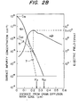
- Fig. 2A is a sectional view showing the MISFET having the double diffused drain structure of the prior art.
- reference numerals 1, 2 and 3 indicate a p-type semiconductor substrate, a field oxide and a gate oxide, respectively.
- numerals 5 to 8 indicating n-type diffused layers formed by using a gate electrode 4 as a diffusion mask
- numerals 5 and 7 indicate drain diffusion layers
- numerals 6 and 8 indicate source diffusion layers.
- the layers 5 and 6 are the low concentrated diffusion layers which have a surface impurity concentration C S2 and a junction depth X j2 .
- the layers 7 and 8 are the highly concentrated layers which have a surface impurity concentration C s1 and a junction depth X j1 .
- Fig. 2B presents the representative results of both the impurity concentration distribution and the electric field which are plotted against the distance from the drain junction edge to the source junction edge on the substrate surface of the MISFET of Fig. 2A.
- FIG. 2B corresponds to the case in which an effective channel length is 1.1 pm, in which the thickness of the gate oxide 3 is-20 nm, in which X j1 and X j2 are 0.25 ⁇ m and 0.35 pm in which C S1 and C S2 are 1 ⁇ 10 21 cm- 3 and 1 ⁇ 10 19 cm- 3 , and in which the voltages applied to the gate electrode 4 and the drain electrode 9 are 0 V and 10 V, respectively.
- the electric field on the substrate surface is caused to take its maximum in the drain diffusion layers near at an impurity concentration of 10 18 cm- 3 by the application of a drain voltage and to become lower in the drain diffusion layer 7 having a higher impurity concentration.
- the present invention is based upon the founding of the abruptly dropping tendency of the electric field in the highly concentrated diffusion layer 7 as a result of the analyses.
- the result makes it possible to consider that the region 7 in the MISFET of the double diffused drain structure of the prior art has little contribution to raise the breakdown voltage.
- it can be considered from the standpoint of the high breakdown voltage of the MISFET of short channel length that the presence of the highly concentrated diffusion layers rather raises an obstruction and that the drain diffusion layers are made of the low concentrated diffusion layers.
- this concept has not been put into practice yet.
- the sheet resistance of 50 ⁇ / ⁇ by the ordinary highly concentrated diffusion layers can be reduced to one tenth, i.e., 3 ⁇ / ⁇ or lower by the prior art of forming a silicide of platinum or the like on the diffusion layers.
- the sheet resistance reducing effect is noted, but no investigation from the standpoint of improving the source-drain breakdown voltage has not been made in the prior art. Therefore, the highly concentrated diffusion layer having a surface concentration equal to or higher than 10 20 cm- 3 is used as the drain diffusion layer on the basis of the fixed concept.
- the present invention is based upon the investigated results made while considering that the above fixed concept is nonsense and that it is made possible by optimizing the drain diffusion layer and the impurity distribution to raise the source-drain breakdown voltage, to ensure the good ohmic contact between the drain electrode and the drain diffusion layer, and to reduce the sheet resistance. More specifically, the present invention is based upon the finding of the fact that, if the surface concentration of the drain diffusion layer to be formed with the silicide layer is equal to or higher than 10 18 cm- 3 but lower than 10 20 cm- 3 , a precipitation layer having a surface concentration of about 10 19 c m- 3 having a thickness of 10 nm can be formed just below the silicide layer to ensure the ohmic contact sufficient for the ordinary operation of the MISFET.
- the present invention is also based upon the finding of the fact that, if the surface concentration of the drain diffusion layer is lower than 10 20 cm- 3 , the source-drain breakdown voltage can be made higher by 5 . V at the maximum even in the MISFET having an effective channel length of 1 ⁇ m or less than that of the MISFET of the prior art.
- Figs. 3 to 6 are sectional views showing the fabricating steps in the consecutive order in accordance with the first embodiment of the MISFET of the present invention.
- Indicated at reference numeral 1 is a silicon substrate of p-conductive type having a specific resistance of 1 ⁇ cm.
- the semiconductor substrate 1 is selectively formed with a thick field oxide 2 having a thickness of 0.8 pm by making use of the conventional isolation technique. After that, the substrate surface has its active region exposed to the outside to form a clean gate oxide 3 having a thickness of 20 nm. After that gate oxide 3, it is formed thereon a silicon film having a thickness of about 0.3 pm, into which phosphorous is diffused in high concentration by the thermal diffusion using POCI 3 as a source.
- a gate electrode 4 is formed by the lithography.
- the channel length after the lithography is 1 pm.
- silicon oxide 11 having a thickness of 0.5 pm is deposited all over the surface by the chemical vapor deposition using tetraethoxysilane (Si(OC 2 H 5 ) 4 ).
- the deposited film 11 is anisotropically etched in the direction normal to the surface of the semiconductor substrate by the reactive sputter etching thereby to remove the silicon oxide deposited on the flat portion.
- the silicon oxide 11 is left only on the side wall of the gate electrodes 4, as shown in Fig. 4.
- arsenic is injected into the semiconductor substrate 1 through the oxide layer 3 by the ion implantation technique under the acceleration energy of 70 KeV.
- This condition is for ensuring the maximum impurity concentration on the substrate surface.
- a number of MISFETs are so fabricated by using the implantation dose as a variable that the surface impurity concentration takes various values within a range of 1x10¹⁷ to 10 20 cm- 3.
- the injected ions are annealed and activated.
- the annealing step thus far described is conducted at 1,000°C, but annealing times are so set for the respective MISFETs having various implantation dose that the junction depth X j may be 0.25 pm.
- the gate oxide 3 lying on the drain diffusion layer 5 and the source diffusion layer 6 is removed and is evaporated all over surface with platinum (Pt) having a thickness of 50 nm by the sputtering process.
- Pt platinum
- an annealing process at 450°C is conducted to form platinum silicide (PtSi) 12 on the surface of the drain and source diffusion layers 5 and 6 and on the surface of the gate electrode 4.
- PtSi platinum silicide
- no reaction with silicon is caused on the oxides 11 and 2 to produce no silicide.
- an etching process is conducted with aqua regia after the annealing step.
- the PtSi is not etched by the aqua regia, only the unreacted Pt is removed to leave the PtSi in self-alignment only on the respective surfaces of the gate electrode 4, the drain diffusion layer 5 and the source diffusion layer 6.
- a segregated layer 13 in a self-alignment with the PtSi layer 12 that it has a thickness of about 10 nm and it has an impurity concentration of one order higher than the surface impurity concentration before the PtSi layer is formed.
- the depthwise impurity distribution in the segregated layer 13 has a downward bulging curve against the depth.
- a passivation film 15 and an interconnect & electrode including a drain electrode 9 and a source electrode 10 are formed by the known technique in accordance with the desired circuit system.
- the electrodes 9 and 10 are made of evaporated films of aluminum (Al).
- a TiW film 14 is formed in advance before the aluminum interconnection step in the contact hole portion on the PtSi film 12 by simultaneously sputtering Ti and W.
- the respective MISFETs used for the measurements of Fig. 9 are under the same conditions as those of the effective channel length of 1 ⁇ m, the gate oxide 3 having the thickness of 20 nm and the drain junction depth of 0.25 pm, but only the surface impurity concentration of the drain diffusion layer 5 is different.
- the thickness of the gate side wall oxide 11 is controlled so that the drain junction edge may align with the edge of the gate electrode 4.
- the BV DS value takes the maximum and reaches 11.5Vwhen the surface impurity concentration of the drain diffusion layer 5 is near at 5 ⁇ 10 18 cm- 3 .
- the above-specified value indicates that the breakdown voltage can be raised by 4.5 V or more than the BV DS value of the prior art MISFET which is constructed of the drain having a surface impurity concentration of 10 20 cm- 3 or higher and which has an equal junction depth. From Fig. 9, moreover, it is also found that the MISFET of the present invention can raise the breakdown voltage to a level higher by 3.5 V or more than the maximum of the BV DS value of the MISFET having the double diffused drain structure of the prior art, as indicated by a broken curve.
- the characteristics of the double-diffused drain structure shown in Fig. 9 are directed to the MISFET having such a drain diffusion layer that the low concentration distribution 5 has a junction depth X J2 of 0.25 ⁇ m and a surface impurity concentration C. 2 of the shown values and that the high concentration distribution 13 has a junction depth X j1 of 0.15 ⁇ m and a surface impurity concentration C s1 of 1 ⁇ 10 21 cm- 3 .
- the gate oxide 3 has a thickness of 20 nm and the effective channel has a length of 1 ⁇ m.
- the surface impurity concentration of the drain diffusion layer 5 be higher than 10 18 cm- 3 and lower than 10 20 cm- 3 , preferably, about 5 ⁇ 10 18 cm- 3 .
- the MISFET of the present invention which is constructed of the drain diffusion layer under the above conditions, it was possible to realize the high breakdown voltage of 3.5 V or higher in terms of the BV DS value than that of the MISFET having the same small channel length of the prior art and to ensure the good ohmic contact.
- Fig. 7 is a sectional view showing another embodiment of the present invention, in which the gate side wall oxide 11 of the foregoing first embodiment is thinned so that the drain junction edge may be present beneath the gate electrode 4, thus fabricating the MISFET.
- most of the low concentrated region of the drain diffusion layer 5 can be controlled by a gate bias. Transconductances measured of the MISFET S , which were constructed according to the foregoing first embodiment and the present embodiment while sharing the structural parameters of the effective channel length of 1 um, the source and drain junction depths of 0.25 ⁇ m and the gate oxide of 20 nm thickness, and of the FET which was constructed of the source and drain having the highly concentrated distribution only.
- the MISFETs constructed according to the first and present embodiments had normalized transconductances of 0.95 and 0.98, respectively, for the transconductance 1 of the MISFET having the construction of the prior art.
- the value of the transconductance of the MISFET based upon the present embodiment is concerned with the MISFET which is constructed such that about one half of the drain junction depth is covered with the gate electrode 4.
- the MISFET constructed to have its drain junction covered with the gate electrode 4 could retain the transconductance similarto that of the MISFET of the conventional structure and could realize the source-drain breakdown voltage about two times as high as that of the MISFET of the conventional structure.
- the ratio of the low concentrated region of the drain covered with the gate electrode 4 is enlarged in the present embodiment. From the standpoint of reducing the gate capacitor, on the other hand, the ratio is desired to be small. Therefore, this ratio may be determined by the synthetic judgement concerned with the design of the integrated circuit.
- Fig. 8 is a sectional view showing still another embodiment of the present invention.
- the arsenic ion implantation step for forming the low concentrated drain diffusion layer was divided into two sub-steps, at which the ions were implanted with the respective energies of 70 keV and 300 keV. The subsequent steps were based upon the foregoing first embodiment until the MISFET was fabricated.
- the drain diffusion layer was constructed such that the maximum surface concentration of 5 ⁇ 10 18 cm- 3 was established in the substrate surface by the above-mentioned first ion implantation and such that the maximum surface concentration of 5x1017 cm- 3 was established in the semiconductor substrate about 0.16 ⁇ m inside of the surface thereof by the second ion implantation.
- the substrate current of both the MISFET having the same structural parameters as those of the MISFET of the present embodiment and based upon the foregoing first embodiment and the MISFET constructed to have the double diffused drain structure of the prior art were measured to take the maximum values of 9.6 ⁇ 10 -7 A and 1.2x10- 5 A, respectively.
- the fact that the substrate current of the MISFET based upon the present embodiment is smaller by about two orders than that of the MISFET of the conventional structure indicates that the MISFET according to the present .
- the invention is remarkably effective for improving the reliability of the MISFET. More specifically, it is known that the reduction in the substrate current causes reduction in the injection of hot carriers into the gate oxide. This known action is coincident with the countermeasures for making the degradations of the transistor characteristics such as variations of the threshold voltage or increases in the surface state density hard to occur.
- the drain diffusion layer 5 is formed by composing the low concentrated distributions made different by the twice ion implanting sub-steps of the different acceleration energies for the ion implantation.
- the drain diffusion layer may be composed of three or more kinds of low concentrated distributions, and the fabricating step should not be limited to the ion implantation but may resort to the known thermal diffusion process, for example.
- the impurity to form the drain diffusion layer should not be identical, but its combination is arbitrary if it is such an atom as has the same conductive type.
- drain high field is crowded near the surface of drain junction.
- the principle of the present invention is to compose an idealized drain profile which can release the highly crowded field and can distribute the high field over the drain region.
- the drain diffusion layer 5 is constructed in its entirety such that the impurity concentration for the bias of the maximum electric field is about 1 ⁇ 10 18 cm- 3 . It is desirable that the drain diffusion layer 5 is constructed by composing the impurity concentration distribution.
- Fig. 10 is a sectional view showing a further embodiment of the present invention, in which the gate electrode 4 constructed of the silicon film of the foregoing first embodiment is replaced by a metal gate electrode 4 of a Mo thin film.
- This Mo electrode is formed on its surface with a passivation film 18 of silicon nitride in a self-alignment with the gate electrode 4. This formation is conducted by the etching process using the same photo resist.
- the gate structure is well known as the metal gate structure, and its detailed described will be omitted here.
- the low concentrated drain diffusion layer 5 and source diffusion layer 6 are formed thereon with the PtSi layer 12.
- the maximum impurity concentration by the ion implantation is 1x10 2 ' cm- 3 and takes its maximum on the substrate surface.
- the As ion implantation is so executed by varying the acceleration energy of the ion implanter that the junction depth becomes equal to or less than 50 nm. After that, only the high concentrated region 16 is activated by the pulsed lamp anneal. After that, the passivation film 15, the drain electrode 9 and the source electrode 10 are formed in accordance with the foregoing first embodiment.
- the Ti-W mixed film 14 for preventing any reaction between the aluminum and the silicide in accordance with the foregoing first embodiment.
- the BV DS values were measured of the various MISFETs which has the highly concentrated region 16 having a junction depth of 10 nm to 50 nm in accordance with the above-mentioned structure. In any of the MISFETs, the BV os values were lower by about 0.5 V at most than the BV DS value of the MISFET based upon the foregoing first embodiment.
- the results thus far described have revealed that the source-drain breakdown voltage can be drastically improved better than the MISFET of the prior art structure if the highly concentrated region 16 just beneath the silicide layer 12 has a thickness equal to or less than 50 nm.
- the principle of the present embodiment is that the high breakdown effect of the BV DS value is not effectively troubled while the good ohmic contact being retained if the highly concentrated region 16 formed on the surface of the drain diffusion layer 5 is remarkably thin to have a thickness of 50 nm or less in terms of the junction depth.
- the present embodiment presents an example in which the silicide layer 12 is formed on the drain diffusion layer 5.
- the silicide layer should not be limited to the platinum silicide but may be replaced by either a refractory metal such as Mo, W, Pt, Pd, Ni, Ti, Ta, Nb, Cr or Pr or their silicide films.
- a refractory metal such as Mo, W, Pt, Pd, Ni, Ti, Ta, Nb, Cr or Pr or their silicide films.
- the diffusion layers providing the source and drain regions are thin and have low impurity concentrations, and the silicide layer for reducing the resistances of the diffusion layers is formed apart (i.e., offset) from the gate electrode.
- the MISFET having such offset structure has its effective transconductance reduced to a lower level than that of the MISFET which has its source and drain made of highly concentrated diffusion layers. Therefore, if the gate side wall insulator (which is indicated at numeral 11 in Figs.
- the present invention is based upon the analytical results which trace back to the physical base of the highly concentrated region in the drain diffusion layer without sticking to the existing common sense.
- the impurity concentration of the drain diffusion layer surface is highly doped to its depth of about 10 nm as far as the drain diffusion layer is formed of an n-conductive type impurity such as phosphorous (P) or arsenic (As).
- the impurity concentration of the drain diffusion layer surface is equal to or higher than 1 ⁇ 10 18 cm- 3 , good ohmic characteristics are obtained between the silicide layer and the substrate surface so that no problem arises in the characteristics as the NMOS.
- the drain diffusion layer in the ordinary MISFET has a highly concentrated region of 10 20 cm- 3 or higher near at the semiconductor substrate surface and such an impurity concentration distribution as has its concentration decreased inwardly of the substrate in accordance with the Gaussian distribution or an error function distribution.
- a voltage is biased to the ordinary drain diffusion layer, and the bias field is analyzed as a function of the impurity concentration.
- the latter role i.e., the good ohmic contact with the interconnect metal can be replaced by the structure of the drain diffusion layer having a surface impurity concentration equal to or higher than 1 ⁇ 10 18 cm -3 and the silicide layer on the diffusion layer.
- the former role i.e., the reduction in the source diffused resistor and the drain diffused resistor, it is known to be realized by making a silicide on the surfaces of the source and drain diffusion layers. The effect of reducing the resistance by the silicide is prominent especially in the formation of an extremely shallow junction in the sub-micron-channel-length MISFET.
- the CMOSFET of the present invention develops the concept based upon the above analytical results and makes use of the results which are obtained by replacing the highly concentrated region of the drain diffusion layer by a thin silicide layer junctioned to the drain diffusion layer by the ohmic contact and by analytically determining the most proper condition for the impurity concentration of the drain diffusion layer. That most proper condition is intended to attain high breakdown voltage characteristics of the sub-micron-channel-length MISFET having a gate length of 0.5 um or less and to protect against the latch-up of the same.
- Figs. 11 and 12 plot the respective analytical results of the present invention. There are plotted curves of the source-drain breakdown voltage and the maximum substrate current which were attained as functions of the impurity concentration of the drain diffusion layer surface. In Fig. 11, the avalanche breakdown voltage and the punch-through voltage are depicted by broken lines and solid lines, respectively, as the source-drain breakdown voltage. Those two voltages are determined as the functions of the channel length.
- the avalanche breakdown voltage is concerned with the PMOS, and the values of the NMOS have a tendency that they are lower by 0.5 to 1 (V) as a whole than the shown curves.
- the punch-through voltage there is found no difference between the respective values of the PMOS and NMOS.
- the CMOSFET having a channel length of 0.5 ⁇ m or more is enabled to realize the breakdown voltage of 10 V or higher, which is about two times as high as the source-drain breakdown voltage in the MISFET of the ordinary structure and of the same size, if the surface impurity concentration of the drain diffusion layer is set at 3x10 18 cm- 3 .
- the MISFET having a channel length of 0.4 ⁇ m or less moreover, the most proper surface impurity concentration of the drain diffusion layer is present in dependence upon the channel length.
- the source-drain breakdown voltage can be improved up to about 7 V if the impurity concentration of the drain diffusion layer surface is set at about 1 ⁇ 10 18 cm- 3 .
- a breakdown voltage of about 5 V can be attained if the impurity concentration of the drain surface is set at 5x1017 cm - 3 .
- the substrate current in which the minority carriers induced by the drain current will flow to the substrate, is determined as a function of the gate bias, and its maximum value, i.e., the maximum substrate current is analyzed as a function of the impurity concentration of the drain diffusion layer surface.
- the junction depth of the source and drain diffusion layers is used as a parameter, and the drain voltage is 5 V.
- Fig. 12 It is newly cleared from Fig. 12 that the substrate current can be drastically improved from that of the ordinary structure, although it depends more or less upon the drain junction .depth, if surface concentration of the drain diffusion layer is set at 10 17 to 10 18 cm- 3 , so that the protection of the latch-up phenomenon can be expected.
- the present invention has succeeded in realizing the sub-micron-channel-length CMOSFET which has such a high breakdown voltage and a latch-up protection as have never been attained.
- the PMOS is formed of the drain junction of the Schottky barrier based upon the above two papers.
- the drain junction is formed by the combination of the diffusion layer having a surface impurity concentration of 10 18 cm- 3 or higher and the silicide layer having the ohmic contact on the basis of the new analytical result obtained from Fig. 11.
- the surface impurity concentrations of the respective source and drain diffusion layers of the PMOS and the NMOS can be made the most proper for the high breakdown voltage of the sub-micron-channel-length CMOSFET having a channel length of 0.5 ⁇ m or less.
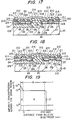
- Figs. 13, 14 and 15 are sectional views showing the fabricating steps of fabricating the CMOSFET according to the fifth embodiment of the present invention.
- reference numeral 21 indicates an n-conductive type silicon substrate having a specific resistance of 0.4 ⁇ cm, in which boron is diffused in a predetermined position to have a junction depth of 2 ⁇ m and a surface impurity concentration of 1 ⁇ 10 16 cm- 3 to form a p-conductive type well 22.
- a thick field oxide 23 having a thickness of 0.5 pm is selectively formed by making use of the known isolation method. After that, the semiconductor surface in the active region is exposed to form a clean gate oxide 28 having a thickness of 20 nm.
- a silicon film having a thickness of about 0.4 pm is formed on the gate oxide 28, and phosphorous is diffused in a high concentration into the silicon film by the thermal diffusion using POCI 3 as an impurity source.
- the silicon film has its surface thermally oxidized to form a silicon oxide having a thickness of 0.2 pm on the silicon film.
- the silicon oxide and silicon film are simultaneously etched by the lithography in accordance with the desired circuit construction to leave a gate passivation film 212 and a gate electrode 29.
- five conditions of 1.0, 0.5, 0.3, 0.2 and 0.1 ⁇ m were executed as the length of the gate electrode 29, i.e., the channel length after the lithography.
- a silicon oxide having a thickness of 0.3 ⁇ m is deposited all over the surface by the chemical vapor deposition using tetraethoxysilane (Si(OC 2 H 5 ) 4 ).
- the deposited film is etched in a direction normal to the surface of the semiconductor substrate by the reactive sputter etching process to remove the deposited film' of silicon oxide on the flat portion.
- a deposited silicon oxide 213 is left only on the respective side wall portions of the gate electrode 29 and the field oxide 23.
- a photo resist film having a thickness of 0.8 ⁇ m is left on the gate oxide 28 excepting the region of the well 22, and arsenic ions are implanted under the condition of an acceleration energy of 70 keV.
- This ion implantation is under the condition in which it is conducted upon the well region 22 through the gate oxide 28 so that the maximum impurity concentration is attained on the surface of the semiconductor substrate.
- the ions to be injected are blocked by the photo resist film so that they are not injected into the semiconductor substrate 21.
- the left photo resist film is removed.
- the ions implanted are activated and annealed to form n-conductive type source 24 and drain 25 (as shown in Fig. 13).
- the dose of the arsenic ions is so set that the respective surface impurity concentrations of the source and drain diffusion layers 24 and 25 may take 3 ⁇ 10 18 cm- 3 in the case of a channel length of 0.5 ⁇ m or more and 1 ⁇ 10 18 cm- 3 in the case of a channel length of 0.3 pm or less.
- the annealing condition is so controlled that the source diffusion layer 24 and drain diffusion layer 25 may finally have a junction depth of 0.25 ⁇ m. After the annealing process, only the well 22 is covered with the photo resist film having a thickness of 0.8 pm, and boron ions are implanted under a condition of an acceleration energy of 70 keV.
- the boron ions are injected into the semiconductor substrate 21 other than the well 22 through the gate oxide 28 so that the maximum impurity concentration is located on the surface of the semiconductor substrate 21.
- the ion injection is blocked by the photo resist film so that the ions are not injected into the semiconductor substrate 21.
- the left photo resist film is removed, and the boron ions implanted are activated and annealed to form p-conductive type source 26 and drain 27 (as shown in Fig. 14).
- the dose of the boron injection is so set that the surface impurity concentrations of the source and drain diffusion layers 26 and 27 may finally fall under three kinds of conditions of 3x1017 cm- 3 , 1 ⁇ 10 18 cm- 3 and 3 ⁇ 10 18 cm -3 .
- the annealing condition is so controlled that the junction depth of the source and drain diffusion layers 26 and 27 may finally have a junction depth of 0.25 pm.
- the gate oxide exposed on the semiconductor substrate 21 is removed, and platinum (Pt) having a thickness of 50 nm is evaporated all over the surface by the sputter process, followed by an annealing process at 450°C.
- a platinum silicide (PtSi) layer 214 is formed in a self-alignment on the respective surface portions of the source diffusion layers 24 and 26 and drain diffusion layers 25 and 27, to which the surface of the semiconductor substrate 21 is exposed.
- the silicide layer 214 is not formed because the platinum (Pt) does not react on the field oxide 23, the deposited side wall oxide 213 and the passivation film 212.
- the platinum (Pt) is etched all over the surface with aqua regia.
- the platinum silicide (PtSi) is not removed by the aqua regia but is left in a self-alignment only on the source diffusion layers 24 and 26 and on the drain diffusion layers 25 and 27.
- the platinum silicide (PtSi) layer 214 just beneath the platinum silicide (PtSi) layer 214 in the n-conductive type source and drain diffusion layers 24 and 25, there is formed in a self-alignment with the platinum silicide (PtSi) layer 214 a segregated layer having a thickness of about 10 nm, which has an impurity concentration higher by one order than the surface concentration before the platinum silicide layer is formed.
- a silicon oxide 210 having a thickness of about 500 nm is deposited all over the surface by the chemical vapor deposition of monosilane (SiH 4 ) and oxygen (0 2 ), and the silicon oxide 210 is selectively removed by the lithography from such portions of the source diffusion layers 24 and 26 and the drain diffusion layers 25 and 27 as are to be formed with contact holes.
- the silicon oxide 210 has been selectively removed, the whole surface is coated with a TiW film 215 by simultaneously sputtering titanium (Ti) and tungsten (W) while leaving the photo resist film, which has been used at the above step, as it is. After that, the photo resist film is removed.
- an interconnect 211 of aluminum (AI) is formed in accordance with the desired circuit construction (as shown in Fig. 15).
- the TiW film 215 is necessary for preventing any reaction between the aluminum interconnect 211 and the silicide layer 214.
- the following results were attained by measuring the breakdown voltages between the source and drain diffusion layers as to the CMOS-FETwhich was fabricated by the steps described in the above. More specifically, the PMOS, in which the surface impurity concentrations of the respective source and drain diffusion layers 26 and 27 of the p-conductive type were set at 3 ⁇ 10 17 cm- 3 , exhibited the Schottky characteristics, but the MOSFET having a channel length of 0.2 pm or more could attain a breakdown voltage of about 5 V. This value is two times as high as or higher than that of the MOSFET of the prior art structure having a p-conductive type drain surface impurity concentration of 10 19 cm- 3 or higher.
- the PMOS having a p-conductive type drain surface impurity concentration set at 1 ⁇ 10 18 cm- 3 exhibited the transistor characteristics based upon the p + n junction, and its source-drain breakdown voltage was 6.5 to 7 V for the MOSFET having a channel length of 0.3 pm or more. That voltage value is 1.6 to 1.7 times as high as that of the prior art and indicates that the high breakdown effect could be realized.
- the PMOS having the p-conductive type drain surface impurity concentration set at 3 ⁇ 10 18 cm- 3 also exhibited the transistor characteristics based upon the p"n junction, and its source-drain breakdown voltage was about 12 V for the MOSFET having a channel length of 0.5 ⁇ m or more. That voltage value is higher by 2 V or more than that of the prior art and indicates that the high breakdown effect could be realized.
- the MOSFET having a channel length of 0.5 ⁇ m or more had a source-drain breakdown voltage of about 10 V. This value is about two times as high as that of the prior art, and the breakdown voltage is raised.
- the drain surface impurity concentration set at 1 ⁇ 10 18 cm- 3 too, good ohmic characteristics could be retained between the source and drain diffusion layers 24and 25 and the silicide layer 214, and the transistor characteristics based upon the n + p junction were obtained.
- the source-drain breakdown voltage was so dependent upon the channel length such that it took about 6 V for the MOSFET having the channel length of 0.3 ⁇ m and about 3 V for the MOSFET having the channel length of 0.2 ⁇ m. These voltage values are two times as high as or higher than the source-drain breakdown voltage of the NMOS of the prior art structure and raise the breakdown voltage.
- the source-drain breakdown voltages of the NMOS and the PMOS oftheCMOSFET based upon the present embodiment are remarkably identical to the analytical results shown in Fig. 11 sothatthe validity of the analysis has been verified. According to the present embodiment, more specifically, the source-drain breakdown voltage of the sub-micron-channel-length CMOSFET having a channel length of 0.5 um or less could be improved to a value twice as high as that of the prior art.
- the MOSFET is completed in accordance with the present embodiment by setting the surface impurity concentration of the respective source and drain diffusion layers of the NMOS and the PMOS at 3x1018 cm -3 , in the case of the CMOSFET having the channel length of 0.5 ⁇ m or more, and at 1 ⁇ 10 18 cm- 3 in the case of the CMOSFET having the channel length of 0.3 ⁇ m. Then, it is possible to fabricate the sub-micron-channel-length CMOSFET having the high breakdown voltages of 10 V and 6 V, respectively.
- the MOSFET is completed in accordance with the present embodiment by setting the surface impurity concentrations of the source and drain diffusion layers of the PMOS and the NMOS, respectively, at 3 ⁇ 10 17 cm- 3 and 1 ⁇ 10 18 cm- 3 . Then, it is possible to attain the sub-micron-channel-length CMOSFET having the source-drain breakdown voltage of 3 V.
- the Schottky barrier which raises no problem in the characteristics. That Schottky barrier rather has a function to improve the latch-up protecting characteristics.
- the latch-up protecting characteristics are evaluated as to the CMOSFET which has been fabricated by the steps described in the present ' embodiment.
- the following items are measured as the latch-up protecting characteristics. Specifically, the product ⁇ N ⁇ Bp of the current gain ⁇ N of a parasitic NPN bipolar transistor, which used the drain diffusion layer 25 of the NMOS as its emitter, the well 22 as its base, and the semiconductor substrate 21 as its collector, and the current gain Pp of a parasitic PNP transistor which used the source diffusion layer 26 of the PMOS as its emitter, the semiconductor substrate 21 as its base, and the well 22 as its collector, was measured.
- the most proper condition of the drain surface impurity concentration of the NMOS may be set in accordance with the desired channel length not from the standpoint of protecting the latch-up but rather from the standpoint of improving the source-drain breakdown voltage.
- the CMOSFET which had the respective NMOS and PMOS drain surface impurity concentrations set at 5 ⁇ 10 18 and 10 2 ° cm- 3 and which had a channel length of 0.2 to 1.0 um, was fabricated, and its source-drain breakdown voltages and latch-up protecting characteristics were measured.
- the source-drain breakdown voltage of the above-specified CMOSFET was improved by several volts at the maximum from the value of the prior art, and the product ⁇ N ⁇ ⁇ P was smaller than 1, but the characteristics were slightly inferior to those of the aforementioned results.
- Figs. 16 and 17 are sectional views showing the steps of fabricating the CMOSFET according to the sixth embodiment of the present invention.
- the deposited silicon oxide 213 is left in self-alignment only on the side walls of the gate electrode 29 and the field oxide 23, and the exposed gate oxide is completely removed.
- a chemical vapor deposition of dichlorosilane (SiH 2 Cl 2 ) and hydrochloric acid (HCI) is conducted at a temperature of 775°C to deposit the polycrystalline or amorphous thin silicon film 216 having a thickness of 0.3 ⁇ m selectively on the surfaces of the well 22 and the semiconductor substrate 21 held in the n-type conductivity (as shown in Fig. 16).
- the forming condition of the deposited silicon film is exemplified by the deposition rate of 10 nm/minute for 200 cc of dichlorosilane and 60 cc of hydrochloric acid. Under this condition, so long as the silicon nitride film (Si 3 N 4 ) is not present on the surface of the deposited film, the deposition is selectively effected on the silicon substrate only, and a smooth flat shape can be obtained even at the boundary with the side wall insulation film 213.
- the photo resist film is so selectively formed that an ion implantation may be effected only at the thin silicon film of the well 22, and a boron ion implantation is executed.
- the dose of the boron injection is so set that the impurity concentration in the thin silicon film 216 may coincide with that on the surface of the well 22.
- the implanting energy is 25 keV.
- the coefficient of diffusion of an impurity in the thin silicon film 216 is 10 to 20 times as large as that in the single crystalline - silicon.
- the boron ions injected into the thin silicon film 216 on the well 22 are distributed substantially uniformly in the depthwise direction within the thin silicon film 216 by the short annealing process.
- the n-conductive type source and drain diffusion layers 24 and 25 and the p-conductive type source and drain diffusion regions 26 and 27 are formed.
- the thin silicon film 216 has already been made into a single crystal by the short time and high temperature annealing process. Therefore, the conditions for forming the respective source and drain diffusion layers are the same as those in the case of the foregoing fifth embodiment.
- the CMOSFET is fabricated in accordance with the fifth embodiment (as shown in Fig. 17).
- the CMOSFET based upon the sixth embodiment shown in Fig. 17 has the same size as that of the CMOSFET based upon the foregoing fifth embodiment.
- the source-drain breakdown voltages of the two CMOSFETs were compared to reveal that the CMOSFET of the sixth embodiment under the conditions of the channel length of 0.3 Ilm and the source and drain surface impurity concentrations of 1x10 18 cm- 3 had a breakdown voltage of 7 V which was higher by about 1 V than that of the CMOSFET of the foregoing fifth embodiment.
- the breakdown voltage of the CMOSFET of the sixth embodiment which was constructed under the conditions of the channel length of 0.2 jjm and the NMOS and PMOS drain surface impurity concentrations of 1 ⁇ 10 18 cm- 3 and 3x1017 cm- 3 , was measured and compared with that of the CMOSFET of the foregoing fifth embodiment. Then, the former breakdown voltage was higher by about 2 V and took a value of 5 V. This value implies that the breakdown voltage was realized to be three times or more as high as the source-drain breakdown voltage of the CMOSFET based upon the prior art structure. In the CMOSFET based upon the sixth embodiment, the product f3 N .
- ⁇ P of the current gains of the parasitic bipolar transistor was measured in case the channel length had various values and the source-drain surface impurity concentration had various values, and that product was reduced two to one half of the measured value of the CMOSFET based upon the foregoing fifth embodiment.
- the CMOSFET based upon the sixth embodiment is improved better in the source-drain breakdown voltage and in the latch-up protecting characteristics than the CMOSFET based upon the fifth embodiment.
- the reason for this improvement can be explained by the fact that the junction area was decreased but the effective channel length was increased by forming the respective source and drain junctions in the thin semiconductor film 216.
- Figs. 20 and 21 are a sectional view showing the CMOSFET according to the seventh embodiment of the present invention and a diagram plotting the impurity concentration distribution in the depthwise direction in the n-conductive type drain diffusion region.
- the polycrystalline or amorphous silicon film 216 is deposited in self-alignment on the semiconductor substrate 21. After that, a photo resist film is so left on the surface of the region other than the silicon film 216 that the ion implantation may be effected only on the portion of the silicon film of the well 22. After that, arsenic ions are implanted in the 'portion of the silicon film on the well 22, and the left photo resist film is then removed.
- the well 22 is covered with the photo resist film, and this photo resist film is left again so that the ion implantation may be effected only on the silicon film on the semiconductor substrate 21 of n-conductive type other than the well 22.
- boron ions are implanted, and the photo resist film is removed again completely to expose the silicon film 216.
- the short time and high temperature annealing process is executed at 1,100°C for 30 seconds, even with this annealing process under the specified conditions, the silicon film 216 is not made into a single crystal but is held in its polycrystalline or amorphous state.
- the coefficient of diffusion of the impurity in the polycrystalline or amorphous silicon film 216 has such a remarkably large value as has been described hereinbefore, the arsenic and boron ions are distributed at a high speed to take a uniform concentration in the silicon film 216 by the above-specified short time annealing process.
- the coefficient of diffusion of each impurity in the semiconductor substrate 21 is relatively small so that the impurities are diffused by about 20 nm at most within the semiconductor substrate 21 even by the short time annealing process.
- the silicon film 216, the well 22 and the n-conductive type semiconductor substrate 21 are formed therein with the n-conductive type source and drain diffusion layers 24 and 25 and the p-conductive type source and drain diffusion layers 26 and 27, respectively.
- the platinum silicide (PtSi) layer 214 is formed in self-alignment on the source diffusion layers 24 and 26 and drain diffusion layer 25.
- the impurity concentration distributions of the n-conductive type source and drain diffusion layers 24 and 25 of the CMOSFET according to the seventh embodiment are divided, as shown in Fig. 19 into three regions A, B and C, i.e., an impurity segregated region A having a thickness of about 10 nm and lying just beneath the silicide layer 214, a uniform distribution region B inside of the silicon film 216, and a steep concentration gradient region C having a junction depth of about 20 nm in the well 22.
- the impurity segregated region A is not found in the p-conductive type source and drain diffusion layers 26 and 27.
- the MOSFET was fabricated by setting the dose of the arsenic or boron implantation such that the uniform distribution concentration in the silicon film 216 might take the respective values of 1 ⁇ 10 18 cm- 3 , 3 ⁇ 10 18 cm- 3 , 10 19 cm - 3 and 5 ⁇ 10 19 cm -3 for the NMOS and the respective values of 1x10" cm- 3 , 3x1017 cm- 3 , 1 ⁇ 10 18 cm- 3 , 3 ⁇ 10 18 cm- 3 and 5x10 18 cm- 3 for the PMOS.
- the MOSFET was fabricated in case the channel length took the respective values of 0.1, 0.2, 0.3, 0.5 and 1.0 ⁇ m.
- the source-drain breakdown voltages and the product ⁇ N ⁇ ⁇ P of the respective current gains of the parasitic bipolar transistors were measured.
- the uniformly distributed impurity concentration in the drain diffusion layer 27 of the NMOS was equal to or more than 10 19 cm- 3 , the improvement in the characteristics were not found.
- the uniformly distributed impurity concentration was set at a low value of 10 17 to 10 19 cm -3 ; the improvement especially in the source-drain breakdown voltage was prominent.
- the source-drain breakdown voltage of the respective CMOSFETs having channel lengths of 0.1 and 0.2 pm reached as high as 4.5 and 8 V, respectively.
- These values were drastically improved better than those of the case of the CMOSFET based upon the sixth embodiment. This effect was relatively prominent in the case of the smaller channel length.
- the uniformly distributed impurity concentration in the drain diffusion layer 25 in the PMOS was lower than 10 17 to 10 18 cm- 3 and the gate length was 0.1 ⁇ m, the source-drain breakdown voltage was improved by several volts better than that in the case of the sixth embodiment to reach 5 V or higher.
- the difference in the effect between the seventh and sixth embodiments can be explained to come from the fact that the low concentrated region to be biased with the maximum drain field is formed substantially uniformly in the silicon film 216, as shown in Fig. 19 in the case of the seventh embodiment so that the release effect of the field crowding becomes prominent.
- the impurity concentration distribution shown in Fig. 19 is intrinsic to the case in which the silicon film 216 is made of a polycrystalline or amorphous material. This construction remarkably enhances the source-drain breakdown voltage of the sub-micron-channel-length CMOSFET.
- the product ⁇ N ⁇ ⁇ P of the parasitic bipolar transistors of the sub-micron-channel-length CMOSFET based upon the seventh embodiment was not substantially different from that of the case of the eighth embodiment, and the latch-up phenomenon was negligible.
- the surface conductivity beneath the side wall insulator 213 might be controlled, if desirable, by the way of ion implantation technique before forming side wall insulators.
- the position of the maximum field can be widely dispersed within the . drain diffusion layer so that the source-drain breakdown voltage can be improved by 5 V or more better than that of the transistor of the prior art structure having the same structural parameters.
- a transistor of miniaturized structure having an effective channel length of 0.5 ⁇ m or less can be operated without any change such as a drop of the power supply voltage from 5 V to 3 V or lower.
- the impurity concentration region necessary for the ohmic contact is constructed in self-alignment with the PtSi layer by making use of the segregation effect of the impurity just beneath the PtSi layer when this layer is to be formed.
- This PtSi layer may be replaced by another refractory metal such as Mo, W, Pd, Ni, Ti, Ta, Nb, Cr or Pr or their silicide film.
- the source-drain diffusion layers were made of the As ions, for example, but may be made of P ions.
- the method of forming the diffusion layers should not be limited to the ion implantation but may resort to another known method such as the thermal diffusion method without departing from the scope of the present invention. Still moreover, the present invention should not be limited to the single transistor thus far described but can also be applied to a semiconductor integrated circuit device.
- the effects of the fifth to seventh embodiments are obtained by improving the regions corresponding to the source and drain of the existing structure. But, the breakdown voltage is not raised by increasing the concentration of the semiconductor substrate 21. As a result, the mobility is neither degraded on the basis of the increase in the substrate doping concentration, nor is degraded the high speed operation.
- the refractory metal or its silicide layer is formed on the source and drain diffusion layers.
- the submicron- channel-length CMOSFET can retain its sheet resistance at a low level, e.g., at several ⁇ / ⁇ so that the high speed operation can be ensured.
- the platinum silicide (PtSi) layer was formed in self-alignment on the source and drain diffusion layers.
- the PtSi layer was presented, by way of example, and can be replaced by a refractory metal, e.g. Mo, W, Pd, Ni, Ti, Ta, Nb, Cr or Pr or their silicide film.
- a refractory metal e.g. Mo, W, Pd, Ni, Ti, Ta, Nb, Cr or Pr or their silicide film.
- the description has been directed to the method by which a hot temperature furnace was used for the short time annealing process. However, this step may resort to another method such as a lamped annealing process or a laser or electron beam radiation process.
- the descriptions of the respective embodiments are directed to the case in which the p-conductive type well is used.
- the present invention can be applied to the CMOSFET of the structure in which the n-conductive type well is formed in the p-conductive type semiconductor substrate.
Landscapes
- Insulated Gate Type Field-Effect Transistor (AREA)
- Metal-Oxide And Bipolar Metal-Oxide Semiconductor Integrated Circuits (AREA)
- Thin Film Transistor (AREA)
Claims (8)
Applications Claiming Priority (4)
| Application Number | Priority Date | Filing Date | Title |
|---|---|---|---|
| JP55075/83 | 1983-04-01 | ||
| JP58055075A JPS59205759A (ja) | 1983-04-01 | 1983-04-01 | Mis型電界効果トランジスタ |
| JP58121185A JPS6014461A (ja) | 1983-07-04 | 1983-07-04 | 相補型絶縁ゲート電界効果トランジスタの製造方法 |
| JP121185/83 | 1983-07-04 |
Publications (2)
| Publication Number | Publication Date |
|---|---|
| EP0123936A1 EP0123936A1 (de) | 1984-11-07 |
| EP0123936B1 true EP0123936B1 (de) | 1989-01-11 |
Family
ID=26395924
Family Applications (1)
| Application Number | Title | Priority Date | Filing Date |
|---|---|---|---|
| EP84103566A Expired EP0123936B1 (de) | 1983-04-01 | 1984-03-30 | Halbleiterbauelement |
Country Status (4)
| Country | Link |
|---|---|
| US (1) | US4769686A (de) |
| EP (1) | EP0123936B1 (de) |
| KR (1) | KR910006249B1 (de) |
| DE (1) | DE3476144D1 (de) |
Families Citing this family (88)
| Publication number | Priority date | Publication date | Assignee | Title |
|---|---|---|---|---|
| JPS6153761A (ja) * | 1984-08-24 | 1986-03-17 | Hitachi Ltd | 半導体装置 |
| DE3677627D1 (de) * | 1985-04-24 | 1991-04-04 | Gen Electric | Halbleiteranordnung mit isoliertem gate. |
| US4849802A (en) * | 1986-01-21 | 1989-07-18 | Ibm Corporation | Thermally stable low resistance contact |
| US4978628A (en) * | 1986-11-19 | 1990-12-18 | Teledyne Industries, Inc. | Drail-well/extension high voltage MOS transistor structure and method of fabrication |
| US4796082A (en) * | 1987-03-16 | 1989-01-03 | International Business Machines Corporation | Thermally stable ohmic contact for gallium-arsenide |
| JP2609619B2 (ja) * | 1987-08-25 | 1997-05-14 | 三菱電機株式会社 | 半導体装置 |
| US4907048A (en) * | 1987-11-23 | 1990-03-06 | Xerox Corporation | Double implanted LDD transistor self-aligned with gate |
| US4914500A (en) * | 1987-12-04 | 1990-04-03 | At&T Bell Laboratories | Method for fabricating semiconductor devices which include sources and drains having metal-containing material regions, and the resulting devices |
| IT1216476B (it) * | 1988-02-29 | 1990-03-08 | Sgs Thomson Microelectronics | Processo per l'ottenimento di transitori a canale n per alta tensione, particolarmente per memorie eeprom con tecnologia cmos. |
| US5208472A (en) * | 1988-05-13 | 1993-05-04 | Industrial Technology Research Institute | Double spacer salicide MOS device and method |
| JPH01298765A (ja) * | 1988-05-27 | 1989-12-01 | Fujitsu Ltd | 半導体装置及びその製造方法 |
| US5012100A (en) * | 1988-06-08 | 1991-04-30 | Siemens Aktiengesellschaft | Method and apparatus for investigating the latch-up propagation in complementary-metal-oxide semiconductor (CMOS) circuits |
| US4949136A (en) * | 1988-06-09 | 1990-08-14 | University Of Connecticut | Submicron lightly doped field effect transistors |
| US5063422A (en) * | 1988-06-20 | 1991-11-05 | At&T Bell Laboratories | Devices having shallow junctions |
| US5270252A (en) * | 1988-10-25 | 1993-12-14 | United States Of America As Represented By The Secretary Of The Navy | Method of forming platinum and platinum silicide schottky contacts on beta-silicon carbide |
| US5221853A (en) * | 1989-01-06 | 1993-06-22 | International Business Machines Corporation | MOSFET with a refractory metal film, a silicide film and a nitride film formed on and in contact with a source, drain and gate region |
| US4951100A (en) * | 1989-07-03 | 1990-08-21 | Motorola, Inc. | Hot electron collector for a LDD transistor |
| US5258645A (en) * | 1990-03-09 | 1993-11-02 | Fujitsu Limited | Semiconductor device having MOS transistor and a sidewall with a double insulator layer structure |
| US5283449A (en) * | 1990-08-09 | 1994-02-01 | Nec Corporation | Semiconductor integrated circuit device including two types of MOSFETS having source/drain region different in sheet resistance from each other |
| US5300813A (en) * | 1992-02-26 | 1994-04-05 | International Business Machines Corporation | Refractory metal capped low resistivity metal conductor lines and vias |
| TW232751B (en) * | 1992-10-09 | 1994-10-21 | Semiconductor Energy Res Co Ltd | Semiconductor device and method for forming the same |
| US6624477B1 (en) | 1992-10-09 | 2003-09-23 | Semiconductor Energy Laboratory Co., Ltd. | Semiconductor device and method for manufacturing the same |
| US5501989A (en) * | 1993-03-22 | 1996-03-26 | Semiconductor Energy Laboratory Co., Ltd. | Method of making semiconductor device/circuit having at least partially crystallized semiconductor layer |
| US5539217A (en) * | 1993-08-09 | 1996-07-23 | Cree Research, Inc. | Silicon carbide thyristor |
| US5439831A (en) * | 1994-03-09 | 1995-08-08 | Siemens Aktiengesellschaft | Low junction leakage MOSFETs |
| JP2560637B2 (ja) * | 1994-04-28 | 1996-12-04 | 日本電気株式会社 | 電界効果トランジスタ及びその製造方法 |
| US5675167A (en) | 1994-11-24 | 1997-10-07 | Nippondenso Co., Ltd. | Enhancement-type semiconductor having reduced leakage current |
| JPH09186324A (ja) * | 1995-12-21 | 1997-07-15 | Texas Instr Inc <Ti> | ケイ化物化されたゲートおよび接触体を備えた電力用トランジスタ |
| US5897363A (en) * | 1996-05-29 | 1999-04-27 | Micron Technology, Inc. | Shallow junction formation using multiple implant sources |
| US6236085B1 (en) | 1996-11-11 | 2001-05-22 | Denso Corporation | Semiconductor memory device having high-concentration region around electric-field moderating layer in substrate |
| US5793083A (en) * | 1996-11-25 | 1998-08-11 | Texas Instruments Incorporated | Method for designing shallow junction, salicided NMOS transistors with decreased electrostatic discharge sensitivity |
| US5844276A (en) * | 1996-12-06 | 1998-12-01 | Advanced Micro Devices, Inc. | CMOS integrated circuit and method for implanting NMOS transistor areas prior to implanting PMOS transistor areas to optimize the thermal diffusivity thereof |
| US5852306A (en) * | 1997-01-29 | 1998-12-22 | Micron Technology, Inc. | Flash memory with nanocrystalline silicon film floating gate |
| JP4401448B2 (ja) * | 1997-02-24 | 2010-01-20 | 株式会社半導体エネルギー研究所 | 半導体装置の作製方法 |
| US6838320B2 (en) * | 2000-08-02 | 2005-01-04 | Renesas Technology Corp. | Method for manufacturing a semiconductor integrated circuit device |
| US6936849B1 (en) | 1997-07-29 | 2005-08-30 | Micron Technology, Inc. | Silicon carbide gate transistor |
| US6794255B1 (en) | 1997-07-29 | 2004-09-21 | Micron Technology, Inc. | Carburized silicon gate insulators for integrated circuits |
| US6965123B1 (en) | 1997-07-29 | 2005-11-15 | Micron Technology, Inc. | Transistor with variable electron affinity gate and methods of fabrication and use |
| US7154153B1 (en) | 1997-07-29 | 2006-12-26 | Micron Technology, Inc. | Memory device |
| US6031263A (en) | 1997-07-29 | 2000-02-29 | Micron Technology, Inc. | DEAPROM and transistor with gallium nitride or gallium aluminum nitride gate |
| US6746893B1 (en) | 1997-07-29 | 2004-06-08 | Micron Technology, Inc. | Transistor with variable electron affinity gate and methods of fabrication and use |
| US7196929B1 (en) * | 1997-07-29 | 2007-03-27 | Micron Technology Inc | Method for operating a memory device having an amorphous silicon carbide gate insulator |
| US5886368A (en) | 1997-07-29 | 1999-03-23 | Micron Technology, Inc. | Transistor with silicon oxycarbide gate and methods of fabrication and use |
| US6417110B1 (en) * | 1997-08-23 | 2002-07-09 | Radiant Technologies Inc | Method for constructing heat resistant electrode structures on silicon substrates |
| US6306712B1 (en) * | 1997-12-05 | 2001-10-23 | Texas Instruments Incorporated | Sidewall process and method of implantation for improved CMOS with benefit of low CGD, improved doping profiles, and insensitivity to chemical processing |
| WO2000010198A1 (en) * | 1998-08-11 | 2000-02-24 | Koninklijke Philips Electronics N.V. | Method of selectively forming silicide |
| US6878968B1 (en) * | 1999-05-10 | 2005-04-12 | Semiconductor Energy Laboratory Co., Ltd. | Semiconductor device |
| US6137126A (en) * | 1999-08-17 | 2000-10-24 | Advanced Micro Devices, Inc. | Method to reduce gate-to-local interconnect capacitance using a low dielectric constant material for LDD spacer |
| JP2001119021A (ja) * | 1999-10-20 | 2001-04-27 | Nec Corp | 半導体装置の製造方法 |
| JP3833903B2 (ja) * | 2000-07-11 | 2006-10-18 | 株式会社東芝 | 半導体装置の製造方法 |
| JP4819215B2 (ja) * | 2000-07-24 | 2011-11-24 | ルネサスエレクトロニクス株式会社 | 不揮発性半導体記憶装置およびその製造方法 |
| KR100493206B1 (ko) * | 2001-01-16 | 2005-06-03 | 가부시키가이샤 히타치세이사쿠쇼 | 반도체장치 및 그 제조방법 |
| JP4676069B2 (ja) * | 2001-02-07 | 2011-04-27 | パナソニック株式会社 | 半導体装置の製造方法 |
| US6833556B2 (en) | 2002-08-12 | 2004-12-21 | Acorn Technologies, Inc. | Insulated gate field effect transistor having passivated schottky barriers to the channel |
| US7084423B2 (en) | 2002-08-12 | 2006-08-01 | Acorn Technologies, Inc. | Method for depinning the Fermi level of a semiconductor at an electrical junction and devices incorporating such junctions |
| JP4711595B2 (ja) * | 2002-12-10 | 2011-06-29 | 株式会社半導体エネルギー研究所 | Elディスプレイ及び電子機器 |
| CN100370491C (zh) * | 2002-12-10 | 2008-02-20 | 株式会社半导体能源研究所 | 发光装置及其制作方法 |
| US7615822B1 (en) * | 2002-12-23 | 2009-11-10 | Volterra Semiconductor Corporation | Diffused drain transistor |
| TWI253684B (en) * | 2003-06-02 | 2006-04-21 | Tokyo Electron Ltd | Method and system for using ion implantation for treating a low-k dielectric film |
| US7220633B2 (en) * | 2003-11-13 | 2007-05-22 | Volterra Semiconductor Corporation | Method of fabricating a lateral double-diffused MOSFET |
| US7074659B2 (en) * | 2003-11-13 | 2006-07-11 | Volterra Semiconductor Corporation | Method of fabricating a lateral double-diffused MOSFET (LDMOS) transistor |
| US7163856B2 (en) | 2003-11-13 | 2007-01-16 | Volterra Semiconductor Corporation | Method of fabricating a lateral double-diffused mosfet (LDMOS) transistor and a conventional CMOS transistor |
| US7081655B2 (en) * | 2003-12-03 | 2006-07-25 | Advanced Micro Devices, Inc. | Formation of abrupt junctions in devices by using silicide growth dopant snowplow effect |
| WO2005059971A2 (en) * | 2003-12-15 | 2005-06-30 | Koninklijke Philips Electronics N.V. | Active matrix pixel device with photo sensor |
| US7504327B2 (en) * | 2004-06-14 | 2009-03-17 | Semiconductor Energy Laboratory Co., Ltd. | Method of manufacturing thin film semiconductor device |
| US7745293B2 (en) * | 2004-06-14 | 2010-06-29 | Semiconductor Energy Laboratory Co., Ltd | Method for manufacturing a thin film transistor including forming impurity regions by diagonal doping |
| US7179696B2 (en) * | 2004-09-17 | 2007-02-20 | Texas Instruments Incorporated | Phosphorus activated NMOS using SiC process |
| US7405443B1 (en) | 2005-01-07 | 2008-07-29 | Volterra Semiconductor Corporation | Dual gate lateral double-diffused MOSFET (LDMOS) transistor |
| US8461628B2 (en) * | 2005-03-18 | 2013-06-11 | Kovio, Inc. | MOS transistor with laser-patterned metal gate, and method for making the same |
| US7326609B2 (en) * | 2005-05-06 | 2008-02-05 | Chartered Semiconductor Manufacturing, Ltd. | Semiconductor device and fabrication method |
| US8901699B2 (en) | 2005-05-11 | 2014-12-02 | Cree, Inc. | Silicon carbide junction barrier Schottky diodes with suppressed minority carrier injection |
| US7767515B2 (en) * | 2006-02-27 | 2010-08-03 | Synopsys, Inc. | Managing integrated circuit stress using stress adjustment trenches |
| WO2007105157A2 (en) * | 2006-03-14 | 2007-09-20 | Nxp B.V. | Source and drain formation |
| KR100770536B1 (ko) * | 2006-07-19 | 2007-10-25 | 동부일렉트로닉스 주식회사 | 고전압 반도체 소자 및 이의 제조 방법 |
| JP2008192985A (ja) * | 2007-02-07 | 2008-08-21 | Seiko Instruments Inc | 半導体装置、及び半導体装置の製造方法 |
| US7691693B2 (en) * | 2007-06-01 | 2010-04-06 | Synopsys, Inc. | Method for suppressing layout sensitivity of threshold voltage in a transistor array |
| US7895548B2 (en) * | 2007-10-26 | 2011-02-22 | Synopsys, Inc. | Filler cells for design optimization in a place-and-route system |
| US20090108408A1 (en) * | 2007-10-29 | 2009-04-30 | Synopsys, Inc. | Method for Trapping Implant Damage in a Semiconductor Substrate |
| US9472423B2 (en) * | 2007-10-30 | 2016-10-18 | Synopsys, Inc. | Method for suppressing lattice defects in a semiconductor substrate |
| JP5239548B2 (ja) * | 2008-06-25 | 2013-07-17 | 富士通セミコンダクター株式会社 | 半導体装置及び半導体装置の製造方法 |
| JP4845937B2 (ja) * | 2008-07-24 | 2011-12-28 | 株式会社東芝 | スピンmosfetおよびこのスピンmosfetを用いたリコンフィギュラブル論理回路 |
| US8120058B2 (en) * | 2009-10-28 | 2012-02-21 | International Business Machines Corporation | High-drive current MOSFET |
| KR101990622B1 (ko) | 2011-11-23 | 2019-06-18 | 아콘 테크놀로지스 인코포레이티드 | 계면 원자 단일층의 삽입에 의한 ⅳ족 반도체에 대한 금속 접점의 개선 |
| US9390928B2 (en) | 2013-10-22 | 2016-07-12 | Globalfoundries Inc. | Anisotropic dielectric material gate spacer for a field effect transistor |
| US20160071791A1 (en) * | 2014-09-09 | 2016-03-10 | Globalfoundries Inc. | Multimetal interlayer interconnects |
| US9966141B2 (en) * | 2016-02-19 | 2018-05-08 | Nscore, Inc. | Nonvolatile memory cell employing hot carrier effect for data storage |
| US9620611B1 (en) | 2016-06-17 | 2017-04-11 | Acorn Technology, Inc. | MIS contact structure with metal oxide conductor |
| WO2018094205A1 (en) | 2016-11-18 | 2018-05-24 | Acorn Technologies, Inc. | Nanowire transistor with source and drain induced by electrical contacts with negative schottky barrier height |
Family Cites Families (9)
| Publication number | Priority date | Publication date | Assignee | Title |
|---|---|---|---|---|
| US3590471A (en) * | 1969-02-04 | 1971-07-06 | Bell Telephone Labor Inc | Fabrication of insulated gate field-effect transistors involving ion implantation |
| US4005450A (en) * | 1970-05-13 | 1977-01-25 | Hitachi, Ltd. | Insulated gate field effect transistor having drain region containing low impurity concentration layer |
| FR2130094B1 (de) * | 1971-03-16 | 1977-04-01 | Ibm | |
| US4141022A (en) * | 1977-09-12 | 1979-02-20 | Signetics Corporation | Refractory metal contacts for IGFETS |
| JPS55143068A (en) * | 1979-04-25 | 1980-11-08 | Hitachi Ltd | Insulated gate semiconductor device |
| US4384301A (en) * | 1979-11-07 | 1983-05-17 | Texas Instruments Incorporated | High performance submicron metal-oxide-semiconductor field effect transistor device structure |
| US4339869A (en) * | 1980-09-15 | 1982-07-20 | General Electric Company | Method of making low resistance contacts in semiconductor devices by ion induced silicides |
| US4374700A (en) * | 1981-05-29 | 1983-02-22 | Texas Instruments Incorporated | Method of manufacturing silicide contacts for CMOS devices |
| JPS584924A (ja) * | 1981-07-01 | 1983-01-12 | Hitachi Ltd | 半導体装置の電極形成方法 |
-
1984
- 1984-03-29 KR KR1019840001637A patent/KR910006249B1/ko not_active Expired
- 1984-03-30 DE DE8484103566T patent/DE3476144D1/de not_active Expired
- 1984-03-30 EP EP84103566A patent/EP0123936B1/de not_active Expired
-
1987
- 1987-06-19 US US07/063,785 patent/US4769686A/en not_active Expired - Lifetime
Also Published As
| Publication number | Publication date |
|---|---|
| EP0123936A1 (de) | 1984-11-07 |
| KR840008537A (ko) | 1984-12-15 |
| DE3476144D1 (en) | 1989-02-16 |
| KR910006249B1 (ko) | 1991-08-17 |
| US4769686A (en) | 1988-09-06 |
Similar Documents
| Publication | Publication Date | Title |
|---|---|---|
| EP0123936B1 (de) | Halbleiterbauelement | |
| US5465000A (en) | Threshold adjustment in vertical DMOS devices | |
| US4597824A (en) | Method of producing semiconductor device | |
| US7064399B2 (en) | Advanced CMOS using super steep retrograde wells | |
| US6190978B1 (en) | Method for fabricating lateral RF MOS devices with enhanced RF properties | |
| KR920010131B1 (ko) | 반도체 소자 및 그 제조 방법 | |
| JPH08250728A (ja) | 電界効果型半導体装置及びその製造方法 | |
| JPS5961071A (ja) | 絶縁ゲ−ト型電界効果トランジスタとその製造方法 | |
| US6261932B1 (en) | Method of fabricating Schottky diode and related structure | |
| US5147814A (en) | Method of manufacturing an lddfet having an inverted-t shaped gate electrode | |
| US5107321A (en) | Interconnect method for semiconductor devices | |
| JP2003051581A (ja) | Nmosトランジスタのesdに対するロバストネスを改善するためのチャンネルイオン注入方法 | |
| US5374566A (en) | Method of fabricating a BiCMOS structure | |
| US7189644B2 (en) | CMOS device integration for low external resistance | |
| KR100240615B1 (ko) | 반도체장치의제조방법 | |
| JPH03262130A (ja) | 半導体素子の製造方法 | |
| JPH0321101B2 (de) | ||
| KR100281397B1 (ko) | 초박형 soi 정전기방전 보호 소자의 형성 방법 | |
| JP3454076B2 (ja) | 炭化けい素半導体装置 | |
| JPH04258160A (ja) | 半導体装置 | |
| US5604359A (en) | Parasitic PNP transistor with crystal defect layer in the emitter region | |
| KR100189751B1 (ko) | 반도체장치 및 그의 제조방법 | |
| US6303463B1 (en) | Method for fabricating a flat-cell semiconductor memory device | |
| JPS62130563A (ja) | 半導体装置 | |
| JPS6014461A (ja) | 相補型絶縁ゲート電界効果トランジスタの製造方法 |
Legal Events
| Date | Code | Title | Description |
|---|---|---|---|
| PUAI | Public reference made under article 153(3) epc to a published international application that has entered the european phase |
Free format text: ORIGINAL CODE: 0009012 |
|
| AK | Designated contracting states |
Designated state(s): DE FR GB IT |
|
| 17P | Request for examination filed |
Effective date: 19841220 |
|
| 17Q | First examination report despatched |
Effective date: 19861029 |
|
| GRAA | (expected) grant |
Free format text: ORIGINAL CODE: 0009210 |
|
| AK | Designated contracting states |
Kind code of ref document: B1 Designated state(s): DE FR GB IT |
|
| REF | Corresponds to: |
Ref document number: 3476144 Country of ref document: DE Date of ref document: 19890216 |
|
| ET | Fr: translation filed | ||
| ITF | It: translation for a ep patent filed | ||
| PLBE | No opposition filed within time limit |
Free format text: ORIGINAL CODE: 0009261 |
|
| STAA | Information on the status of an ep patent application or granted ep patent |
Free format text: STATUS: NO OPPOSITION FILED WITHIN TIME LIMIT |
|
| 26N | No opposition filed | ||
| ITTA | It: last paid annual fee | ||
| PGFP | Annual fee paid to national office [announced via postgrant information from national office to epo] |
Ref country code: GB Payment date: 20000225 Year of fee payment: 17 |
|
| PG25 | Lapsed in a contracting state [announced via postgrant information from national office to epo] |
Ref country code: GB Free format text: LAPSE BECAUSE OF NON-PAYMENT OF DUE FEES Effective date: 20010330 |
|
| GBPC | Gb: european patent ceased through non-payment of renewal fee |
Effective date: 20010330 |
|
| PGFP | Annual fee paid to national office [announced via postgrant information from national office to epo] |
Ref country code: FR Payment date: 20020319 Year of fee payment: 19 |
|
| PGFP | Annual fee paid to national office [announced via postgrant information from national office to epo] |
Ref country code: DE Payment date: 20020528 Year of fee payment: 19 |
|
| PG25 | Lapsed in a contracting state [announced via postgrant information from national office to epo] |
Ref country code: DE Free format text: LAPSE BECAUSE OF NON-PAYMENT OF DUE FEES Effective date: 20031001 |
|
| PG25 | Lapsed in a contracting state [announced via postgrant information from national office to epo] |
Ref country code: FR Free format text: LAPSE BECAUSE OF NON-PAYMENT OF DUE FEES Effective date: 20031127 |
|
| REG | Reference to a national code |
Ref country code: FR Ref legal event code: ST |