EP0124092B2 - Elektronische Frankiermaschine und Datenlösch- und -schreibverfahren in einem nichtflüchtigen Speicher - Google Patents
Elektronische Frankiermaschine und Datenlösch- und -schreibverfahren in einem nichtflüchtigen Speicher Download PDFInfo
- Publication number
- EP0124092B2 EP0124092B2 EP84104709A EP84104709A EP0124092B2 EP 0124092 B2 EP0124092 B2 EP 0124092B2 EP 84104709 A EP84104709 A EP 84104709A EP 84104709 A EP84104709 A EP 84104709A EP 0124092 B2 EP0124092 B2 EP 0124092B2
- Authority
- EP
- European Patent Office
- Prior art keywords
- voltage
- signal
- volatile memory
- microprocessor
- output
- Prior art date
- Legal status (The legal status is an assumption and is not a legal conclusion. Google has not performed a legal analysis and makes no representation as to the accuracy of the status listed.)
- Expired - Lifetime
Links
Images
Classifications
-
- G—PHYSICS
- G11—INFORMATION STORAGE
- G11C—STATIC STORES
- G11C16/00—Erasable programmable read-only memories
- G11C16/02—Erasable programmable read-only memories electrically programmable
- G11C16/06—Auxiliary circuits, e.g. for writing into memory
- G11C16/32—Timing circuits
-
- G—PHYSICS
- G07—CHECKING-DEVICES
- G07B—TICKET-ISSUING APPARATUS; FARE-REGISTERING APPARATUS; FRANKING APPARATUS
- G07B17/00—Franking apparatus
- G07B17/00185—Details internally of apparatus in a franking system, e.g. franking machine at customer or apparatus at post office
- G07B17/00314—Communication within apparatus, personal computer [PC] system, or server, e.g. between printhead and central unit in a franking machine
-
- G—PHYSICS
- G07—CHECKING-DEVICES
- G07B—TICKET-ISSUING APPARATUS; FARE-REGISTERING APPARATUS; FRANKING APPARATUS
- G07B17/00—Franking apparatus
- G07B17/00185—Details internally of apparatus in a franking system, e.g. franking machine at customer or apparatus at post office
- G07B17/00362—Calculation or computing within apparatus, e.g. calculation of postage value
-
- G—PHYSICS
- G11—INFORMATION STORAGE
- G11C—STATIC STORES
- G11C16/00—Erasable programmable read-only memories
- G11C16/02—Erasable programmable read-only memories electrically programmable
- G11C16/06—Auxiliary circuits, e.g. for writing into memory
- G11C16/10—Programming or data input circuits
- G11C16/20—Initialising; Data preset; Chip identification
-
- G—PHYSICS
- G11—INFORMATION STORAGE
- G11C—STATIC STORES
- G11C16/00—Erasable programmable read-only memories
- G11C16/02—Erasable programmable read-only memories electrically programmable
- G11C16/06—Auxiliary circuits, e.g. for writing into memory
- G11C16/22—Safety or protection circuits preventing unauthorised or accidental access to memory cells
- G11C16/225—Preventing erasure, programming or reading when power supply voltages are outside the required ranges
-
- G—PHYSICS
- G11—INFORMATION STORAGE
- G11C—STATIC STORES
- G11C16/00—Erasable programmable read-only memories
- G11C16/02—Erasable programmable read-only memories electrically programmable
- G11C16/06—Auxiliary circuits, e.g. for writing into memory
- G11C16/30—Power supply circuits
-
- G—PHYSICS
- G07—CHECKING-DEVICES
- G07B—TICKET-ISSUING APPARATUS; FARE-REGISTERING APPARATUS; FRANKING APPARATUS
- G07B17/00—Franking apparatus
- G07B17/00185—Details internally of apparatus in a franking system, e.g. franking machine at customer or apparatus at post office
- G07B17/00314—Communication within apparatus, personal computer [PC] system, or server, e.g. between printhead and central unit in a franking machine
- G07B2017/00346—Power handling, e.g. power-down routine
-
- G—PHYSICS
- G07—CHECKING-DEVICES
- G07B—TICKET-ISSUING APPARATUS; FARE-REGISTERING APPARATUS; FRANKING APPARATUS
- G07B17/00—Franking apparatus
- G07B17/00185—Details internally of apparatus in a franking system, e.g. franking machine at customer or apparatus at post office
- G07B17/00362—Calculation or computing within apparatus, e.g. calculation of postage value
- G07B2017/00395—Memory organization
- G07B2017/00403—Memory zones protected from unauthorized reading or writing
Definitions
- the present invention relates to electronic postage meters, and to a method and apparatus for controlling the erasure and writing of data in non-volatile memory of an electronic postage meter.
- the present application is related to copending European Application EP-A-0,111,322 in the names of Pitney Bowes, Inc., which describes one type of postage meter in which the present invention may be utilized.
- Electronic postage meters include non-volatile memory capability to store critical postage accounting information. This information includes, for example, the amount of postage remaining in the meter for subsequent printing or the total amount of postage already printed by the meter. Other types of accounting or operating data may also be stored in the non-volatile memory, as desired.
- the non-volatile memory in electronic postage meters provides a storage function accomplished in prior mechanical type postage meters by mechanical accounting registers.
- postage meters with mechanical accounting registers are not subject to the many problems encountered by electronic postage meters. Conditions do not normally occur in mechanical type postage meters that prevent accounting or a printing cycle or which result in the loss of data stored in the mechanical accounting registers.
- mechanical postage meters it is not necessary to electronically monitor the position of the mechanical components associated with the printing of postage. The position is however different with electronic postage meters.
- Conditions can occur in electronic postage meters where information stored in non-volatile memory may be permanently lost. Conditions such as a total line power failure or fluctuation in voltage conditions can cause the microprocessor associated with the meter to operate erratically and either cause erasure of data or the writing of spurious data in the non volatile memory. The erasure of data or the writing of spurious data in the non-volatile memory may result in a loss of information representing the postage funds stored in the meter. Since data of this type changes with the printing of postage and is not permanently stored elsewhere, there is no way to recapture or reconstruct the lost information. Under such circumstances, it is possible that a user may suffer a loss of postage funds.
- microprocessors used in electronic postage meters can be reset and become inoperative below a predetermined voltage level, such microprocessors may become active again at even lower voltage levels.
- the microprocessors may be turned off below a predetermined voltage level and thereafter within a lower range turn on again and be capable of outputting data.
- the microprocessors will again turn off below the lower predetermined range. Because of this unreliable operation with respect to reset or turn off the accounting information within the postage meter can be destroyed by the inadvertent erasing of data or writing of spurious data during a power down cycle when the microprocessor is believed to be inoperative.
- the cost of carefully testing and selecting microprocessor component for postage meters to avoid this problem can greatly increase the cost of such parts, both because of the cost of testing and because of the rejection of the microprocessor devices that exhibit this characteristic.
- United States Patent 3,801,963 for Method and Apparatus for Transferring Data from a Volatile Data Store Upon the Occurrence of a Power Failure in a Computer
- United States Patent 3,959,778 for Apparatus for Transferring Data from a Volatile Main Memory to a Store Unit Upon the Occurrence of an Electrical Supply Failure in a Data Processing System
- United States Patent 3,810,116 for Volatile Memory Protection
- United States Patent 3,980,935 for Volatile Memory Support System.
- an operating voltage variation sensing system for an electronic postage meter using hysteresis for the power down and power up cycles.
- an enable voltage to the non-volatile memory during power up and power down of the meter, it is relatively complex and expensive to implement.
- such circuit utilizes the architecture of the microprocessor to provide the power down cycle threshold voltage, and does not supply a low voltage warning signal and a power down cycle threshold voltage to the microprocessor external therefrom.
- GB-A-2,062,311 discloses a method for controlling the erasure and writing of data in non-volatile memory of an electronic postage meter, comprising the steps of
- GB-A-2,062,311 also discloses apparatus for controlling the erasure and writing of data in non-volatile memory of a microprocessor controlled electronic postage meter, comprising:
- the non-volatile memory of this system is enabled to receive or erase data whenever the source of operating power is above the first threshold value. In some conditions, as discussed above, this may not provide adequate security for memory contents.
- An object of the present invention is to provide a non-volatile memory protection circuit which protects the NVM during power-up and power-down of an electronic postage meter, as well as during normal meter operation.
- a further object of the present invention is to provide a non-volatile memory protection circuit which interacts with the microprocessor during meter operation.
- a still further object of the present invention is to provide a non-volatile memory protection circuit in which a low voltage warning signal and power down cycle threshold voltage are applied to the microprocessor external therefrom.
- a further object of the present invention is to provide a non-volatile memory protection circuit which is reliable and simple in design, yet inexpensive to implement.
- an apparatus for controlling the erasure and writing of data in non-volatile memory of a microprocessor controlled electronic postage meter comprising:
- the apparatus is characterised by low voltage warning means for providing a low voltage warning signal to the microprocessor during the power down cycle when the input voltage has decreased to a preset voltage level, said microprocessor being arranged to supply said memory control signal as a write command subsequent to receiving the low voltage warning signal and prior to removal of said output enable signal, and said non-volatile memory switching means being arranged to supply said bias voltage to allow writing of data only during coincidence between said memory control signal and said output enable signal.
- a method of operating apparatus for controlling the erasure and writing of data in non-volatile memory of an electronic postage meter, comprising the steps of:
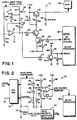
- FIG 1 illustrates a non-volatile memory protection circuit 10 for non-volatile memory (NVM) 58.
- This circuit 10 includes a comparator generally designated as 12 which receives a +23.9V input from a 24V regulator, see Figure 2.
- the comparator 12 includes a first voltage divider 14 having a first resistor 16 electrically coupled between the +23.9V input and the inverting input terminal of an operational amplifier 18, and a second resistor 20 connected between the inverting input terminal of the operational amplifier 18 and ground.
- a second voltage divider 22 includes a resistor 24 coupled between the +23.9V input and one terminal of a Zener diode 26.
- the Zener diode 26 has a breakdown voltage of 6.8V and its other terminal is grounded.
- a second resistor 28 is coupled between the resistor 24 and the non-inverting input terminal of the operational amplifier 18.
- a third resistor 30 is coupled between the resistor 28 and the output of the operational amplifier 18. The resistors 28 and 30 are electrically connected at a reference point designated 31.
- the output of the operational amplifier 18 is coupled to the base terminal of an NPN transistor 32 through a current limiting resistor 34.
- the emitter terminal is grounded and the collector terminal is coupled to a +5V bias through a current limiting resistor 36.
- the output from the collector terminal is applied to a RESET terminal of a microprocessor 38. Also coupled between the collector terminal and ground is a timing capacitor 40.
- a PNP transistor 42 Also coupled to the output of the operational amplifier 18 is a PNP transistor 42.
- the base terminal of the transistor 42 is coupled to the output of the operational amplifier 18 through a current limiting resistor 44.
- the emitter terminal of the transistor 42 is coupled to the collector terminal of a PNP transistor 46.
- the emitter of the transistor 46 is coupled to a +5V bias.
- a resistor 48 is coupled between the emitter and base terminals of transistor 46.
- the base terminal of the transistor 46 is coupled to an ERASE or WRITE control terminal of the microprocessor 38 through a current limiting resistor 50.
- the collector terminal of the transistor 42 is coupled to the base of an NPN transistor 52 through a current limiting resistor 54.
- the emitter terminal of the transistor 52 is coupled to a negative voltage supply, here -30V, and a biasing resistor 56 is coupled between the emitter terminal of a transistor 52 and the collector terminal of transistor 42.
- the collector terminal of transistor 52 is coupled to the NVM 58. Also coupled between the collector terminal of the transistor 52 and ground is a filtering capacitor 60.
- a low voltage warning circuit is illustrated generally at 70. Initially, unregulated D.C. is supplied to a 24V regulator 72 for regulation.
- the output of the 24V regulator 72 is applied to a +5V wide range switching regulator 74, such as a SH1605 available from National Semiconductor Corporation, for providing a constant +5V output when the input voltage is within the range of +8 to +35V.
- An energy storage capacitor 76 is coupled between the output of the +24V regulator 72 and ground.
- the output of the +24V regulator 72 is coupled to the N terminal of a Zener diode 78 having a breakdown voltage of 20V.
- the P terminal of the Zener diode 78 is coupled to the inverting input terminal of an operational amplifier 80 through a current limiting resistor 82.
- Another resistor 84 also couples the P terminal of the Zener diode 78 to ground.
- Another Zener diode 86 having a breakdown voltage of 3.9V has its N terminal coupled to the P terminal of Zener diode 78 and its P terminal coupled to the +24V regulator 72 to provide feedback control of the output voltage from the regulator 72.
- a resistor 88 also couples the P terminal of the Zener diode 86 to ground.
- the non-inverting input terminal of the operational amplifier 80 has a +5V bias applied thereto through a current limiting resistor 90.
- a resistor 92 is also coupled between the non-inverting input terminal of the operational amplifier 80 and ground.
- a feedback resistor 94 is coupled between the output of the operational amplifier 80 and its non-inverting input terminal.
- the output of the operational amplifier 80 is coupled to the low voltage warning terminal of the microprocessor 38.
- the output of the amplifier 80 is normally held at +5 volts through a +5V bias voltage applied thereto through a current limiting resistor 96.
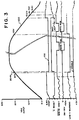
- the D.C. input voltage curve designated 100 is shown with the pertinent voltage signals during power up, power down and normal meter operation related thereto.
- the output COMP of the comparator 12 attains its high state as the input voltage rises toward 6.8V.
- the Zener diode 26 conducts and holds the output of the operational amplifier 18 at a constant 6.8V.
- the transistor 32 conducts providing a RESET signal (true low) to the microprocessor 38.
- the presence of the RESET signal inhibits the microprocessor 38 from generating an ERASE signal until the RESET signal is removed.
- the transistors 46 and 42 are biased out of conduction so that the transistor 52 does not conduct. Therefore, there is no output applied to the -30V terminal of the NVM 58. This condition is true from the time the comparator 12 becomes operational (about 2-3 volts) until the input voltage reaches +20.4 volts.
- the output voltage 102 of the operational amplifier 18 abruptly switches to zero as seen in Figure 3. This is caused by the voltage divider 14 which due to the arrangement of resistors 16 and 20 supplies 1/3 of the input voltage or 6.8 volts to the inverting input terminal of the operational amplifier 18. Since the non-inverting input terminal is also held at 6.8 volts, the operational amplifier 18 switches to a zero volt output. The output of the operational amplifier 18 then remains at zero during the remainder of the power-up cycle and during normal meter operation since the voltage present at the inverting input terminal of the operational amplifier 18 is greater than the voltage present at the non-inverting input terminal. The presence of a zero voltage at the output of the operational amplifier 18 turns off transistor 32 allowing the micro-processor 38 to come out of the reset condition after a short delay provided by timing capacitor 40.
- a low voltage warning signal is supplied to the microprocessor 38 by operational amplifier 80 until the input voltage exceeds 20 volts and Zener diode 78 conducts.
- the switching regulator 74 supplies a positive bias to the non-inverting input of the operational amplifier 80 resulting in a high or warning signal.
- Zener diode 78 starts to conduct causing the output of comparator 80 to go low.
- the microprocessor 38 coming out of the reset condition loops under program control until the output of the operational amplifier 80 goes low indicating the conclusion of a successful power up sequence.
- the microprocessor 38 under program control applies an ERASE ⁇ control signal (true low) to the base terminal of transistor 46. This causes the transistor 46 to conduct providing a positive output voltage at its collector terminal. The presence of the positive output voltage at the collector terminal of the transistor 46 biases the transistor 42 into conduction since its base terminal is held at 0 volts. Thus, a positive voltage appears at the base terminal of transistor 52. Since -30V is present at the emitter terminal, the transistor 52 conducts supplying -30V to the WRITE terminal of the NVM 58 for erasing data therefrom, see Fig. 3.
- the microprocessor 38 provides a WRITE ⁇ control signal to the transistor 46 resulting in the application of -30V to the WRITE terminal of the NVM 58 due to conducticn by the transistor 52.
- data is written into the NVM 38, e.g., from a RAM (not shown).
- the output of the comparator 12 abruptly switches to 6.8V since the voltage on divider 14 falls below the 3.4 volt reference of divider 22. This precludes conduction by the transistors 42 and 52 and thus prevents the application of -30V to the NVM 58. Similar to power up, when the output of the comparator 12 rises to +6.8V, the transistor 32 conducts applying a RESET ⁇ signal to the microprocessor 38 which inhibits the generation of an ERASE signal from the microprocessor 38 until after the RESET ⁇ signal is absent which occurs when the output of the comparator 12 is zero, i.e., at a D. C.
- the transistor 32 conducts applying a RESET ⁇ signal to the microprocessor 38 which further inhibits the generation of a WRITE signal from the micro-processor 38 until a power up cycle is entered.
- the RESET ⁇ signal is high so that the micro-processor 38 can generate a WRITE ⁇ or ERASE ⁇ signal as required for the NVM 58.
- the zero volt enabling signal 102 in Fig. 3 is present at the output of the operational amplifier 18.
- a WRITE ⁇ or ERASE ⁇ signal from the microprocessor 38 will cause the transistors 46 and 42 to conduct. Conduction of transistor 42 causes transitor 52 to conduct. This results in the application of -30V to the NVM 58, enabling the same for the writing of data therein or erasure of data therefrom.
- Some instances in which it may be desired tc erase or write data in NVM during normal meter operation include recharging the registers, e.g., the ascending registers in NVM, changing the combination in VRMRS meters, operating the meter in the service mode to interrogate and change parameters in the NVM, and storing a fault in the NVM.
- postage meter refers to the general class of devices for the imprinting of a defined unit value for governmental or private carrier delivery of parcels, envelopes, or other like application for unit value printing.
- postage meter is utilized, it is employed in the trade as a general term for devices utilized in conjunction with services other than those exclusively employed by governmental postage and tax services.
- private, parcel and freight services purchase and employ such meters as a means to provide unit value printing and accounting for individual parcels.
Landscapes
- Physics & Mathematics (AREA)
- Engineering & Computer Science (AREA)
- General Physics & Mathematics (AREA)
- Mathematical Physics (AREA)
- Theoretical Computer Science (AREA)
- Computer Hardware Design (AREA)
- General Engineering & Computer Science (AREA)
- Computer Security & Cryptography (AREA)
- Techniques For Improving Reliability Of Storages (AREA)
- Devices For Checking Fares Or Tickets At Control Points (AREA)
- Management, Administration, Business Operations System, And Electronic Commerce (AREA)
Claims (10)
- Vorrichtung zur Steuerung des Löschens und Schreibens von Daten in einem nichtflüchtigen Speicher (58) einer durch einen Mikroprozessor gesteuerten elektronischen Frankiermaschine, umfassend:eine Komparatoreinrichtung (12), die dafür eingerichtet ist, an ihrem Ausgang bei einem ersten bestimmten Spannungspegel während eines Einschaltvorgangs zum Anschalten an die Betriebsspannung ein vorbestimmtes Ausgangsfreigabesignal vorzusehen, und das Ausgangsfreigabesignal vom Ausgang während eines Abschaltvorganges von der Betriebsspannung bei einem bestimmten zweiten Spannungspegel zu entfernen, wobei der erste bestimmte Spannungspegel größer ist als der zweite bestimmte Spannungspegel,eine Rücksetzsignaleinrichtung (32) zum elektrischen Verbinden des Ausgangs der Komparatoreinrichtung (12) mit dem Mikroprozessor (38) zur Unterbindung der Erzeugung von Speichersteuersignalen von einem Mikroprozessor-Steueranschluß bei Abwesenheit des vorbestimmten Ausgangsfreigabesignals (102) am Ausgang der Komparatoreinrichtung (12),eine Lösch- und Schreib-Steuereinrichtung (42, 46) zur elektrischen Verbindung zwischen dem Steueranschluß des Mikroprozessors (38) und dem Ausgang der Komparatoreinrichtung (12) undeine Schalteinrichtung (52) für den nichtflüchtigen Speicher, die zur Lieferung einer Vorspannung an den nichtflüchtigen Speicher mit der Lösch- und Schreib-Steuereinrichtung (42, 46) verbunden ist,dadurch gekennzeichnet,
daß die Schalteinrichtung (52) für den nichtflüchtigen Speicher aktivierbar ist, um die Vorspannung wie oben beschrieben zu liefern, so daß die Löschung von Daten vom nichtflüchtigen Speicher zugelassen wird in Ansprechen auf ein Steuersignal von der Lösch- und Schreib-Steuereinrichtung erzeugt bei Konzidenz des Vorhandenseins eines Speichersteuersignals vom Steueranschluß des Mikroprozessors (38) und des Vorhandenseins der vorbestimmten Steuerausgangsspannung am Ausgang der Komparatoreinrichtung (12). - Vorrichtung nach Anspruch 1,
gekennzeichnet durch eine Niedrigspannung-Warneinrichtung (80) zur Abgabe eines Niedrigspannung-Warnsignals an den Mikroprozessor (38) während des Abschaltvorganges, wenn die Eingangsspannung auf einen voreingestellten Pegel abgenommen hat, wobei der Mikroprozessor (38) dazu eingesetzt ist, das Speichersteuersignal als einen Schreibbefehl zu liefern im Anschluß an den Empfang des Niedrigspannung-Warnsignals und vor der Entfernung des Ausgangsfreigabesignals, und die Schalteinrichtung (42, 46) für den nichtflüchtigen Speicher dazu eingesetzt ist, die Vorspannung zu liefern, um das Schreiben von Daten nur während der Koinzidenz zwischen dem Speichersteuersignal und dem Ausgangsfreigabesignal zuzulassen. - Vorrichtung nach Anspruch 2, dadurch gekennzeichnet, daß die Niedrigspannung-Warneinrichtung einen Operationsverstärker (80) und ein Paar Zener-Dioden (78, 86) umfaßt, die mit dem Operationsverstärker elektrisch verbunden sind, um ein Niedrigspannung-Warnsignal an den Mikroprozessor (38) abzugeben, wenn die Eingangsspannung zur Niedrigspannung-Warneinrichtung unter den Wert fällt, bei dem die Spannung an einer der Zener-Dioden zusammenbricht.
- Vorrichtung nach Anspruch 1, 2 oder 3, dadurch gekennzeichnet, daß die Komparatoreinrichtung (12) einen Operationsverstärker (18), eine Zener-Diode (26) und ein Spannungteiler-Netzwerk (24, 28, 30) enthält, wobei die Zener-Diode und das Spannungsteiler-Netzwerk den Wert der vorbestimmten Steuerausgangsspannung festlegen.
- Vorrichtung nach einem der Ansprüche 1 bis 4, dadurch gekennzeichnet, daß die Rücksetzsignaleinrichtung (36) einen Transistor enthält, der durchgeschaltet wird, wenn die vorbestimmte Steuerausgangsspannung am Ausgang der Komparatoreinrichtung (12) nicht vorhanden ist.
- Vorrichtung nach einem der Ansprüche 1 bis 5, dadurch gekennzeichnet, daß die Lösch- und Schreib-Steuereinrichtung ein Paar miteinander verbundene Transistoren (42, 46) enthält zum Empfang eines Steuersignals vom Mikroprozessor (38) als das eine Eingangssignal und das Ausgangssignal der Kompraratoreinrichtung (12) als das andere Eingangssignal.
- Vorrichtung nach einem der Ansprüche 1 bis 6, dadurch gekennzeichnet, daß die Schalteinrichtung des nichtflüchtigen Speichers einen Transistor (52) enthält, wobei eine Steuerspannung an einen ersten Anschluß und der Ausgang der Lösch- und Schreib-Steuereinrichtung (42, 46) an einen zweiten Anschluß angelegt sind, während der dritte Anschluß zur Verbindung mit dem nichtflüchtigen Speicher (58) dient.
- Verfahren zum Betrieb der Vorrichtung nach Anspruch 2 oder 3 oder nach einem der Ansprüche 4 bis 7 in Rückbeziehung auf Anspruch 2 zur Steuerung des Löschens und Schreibens von Daten im nichtflüchtigen Speicher (58) einer elektronischen Frankiermaschine, umfassend folgende Schritte:(a) Darstellen eines gesteuerten Eingangsleistungssignals (100) zur Lieferung eines Ausgangsfreigabesignals (102), wenn das Eingangsleistungssignal während eines Einschaltvorganges zum Anschalten an die Betriebsspannung eine erste vorbestimmte Schwellwertspannung erreicht,(b) Entfernen des Ausgangsfreigabesignals (102) während eines Abschaltvorganges von der Betriebsspannung, wenn das Eingangsleistungssignal unter eine zweite vorbestimmte Schwellwertspannung fällt, welche kleiner ist als die erste vorbestimmte Schwellwertspannung,(c) Übertragung eines Rücksetzsignals (RESET) auf einen Mikroprozessor (38) zur Verhinderung der Erzeugung eines Speichersteuersignals für den nichtflüchtigen Speicher (58), bevor das Eingangsleistungssignal die erste vorbestimmte Schwellwertspannung erreicht,(d) Anlegen einer Vorspannung an einen Anschluß des nichtflüchtigen Speichers (58), um ihn betriebsfähig zu machen,(e) Betreiben des Mikroprozessors in seinem Abschaltvorgang, wenn der zweite vorbestimmte Schwellwert erreicht wird zur Übertragung von Information an den nichtflüchtigen Speicher (58), wonach die Vorspannung vom nichtflüchtigen Speicher abgeschaltet wird, und(f) Übertragen des Speichersteuersignals vom Mikroprozessor (38), nachdem das Eingangsleistungssignal die erste Schwellwertspannung erreicht hat,gekennzeichnet durch- Anlegen der Vorspannung an den Anschluß des nichtflüchtigen Speichers (58) zur Ermöglichung der Löschung von Daten hieraus nur während der Koinzidenz zwischen dem Speichersteuersignal und dem Ausgangsfreigabesignal (102),- Anlegen eines Niedrigspannung-Warnsignals an den Mikroprozessor (38), wenn das Eingangsleistungssignal unter einen bestimmten Wert fällt,- Übertragen des Speichersteuersignals vom Mikroprozessor (38) als einen Schreibbefehl im Anschluß an den Empfang des Niedrigspannung-Warnsignals und vor dem Entfernen des Ausgangsfreigabesignals (102),- Anlegen der Vorspannung an den Anschluß des nichtflüchtigen Speichers (58) zur Ermöglichung des Einschreibens von Daten in Abhängigkeit vom Schreibbefehl nur während der Koinzidenz zwischen dem Speichersteuersignal und dem Ausgangsfreigabesignal und- Anlegen des Rücksetzsignals an den Mikroprozessor (38) in Koinzidenz mit dem Entfernen des Ausgangsfreigabesignals zur Verhinderung der Erzeugung von Schreib- oder Lösch-Störsignalen durch den Mikroprozessor.
- Verfahren nach Anspruch 8,
gekennzeichnet durch das Anlegen einer stabilen Eingangsspannung an den Mikroprozessor (38) während eines normalen Frankiermaschinenbetriebes zwischen den ersten und zweiten vorbestimmten Schwellwertspannungen. - Elektronische Frankiermaschine,
gekennzeichnet durch eine Vorrichtung nach einem der Ansprüche 1 bis 7 in Verbindung mit einem nichtflüchtigen Speicher (58) und einem Mikroprozessor (38).
Applications Claiming Priority (2)
| Application Number | Priority Date | Filing Date | Title |
|---|---|---|---|
| US489971 | 1983-04-29 | ||
| US06/489,971 US4534018A (en) | 1983-04-29 | 1983-04-29 | Non-volatile memory protection circuit with microprocessor interaction |
Publications (4)
| Publication Number | Publication Date |
|---|---|
| EP0124092A2 EP0124092A2 (de) | 1984-11-07 |
| EP0124092A3 EP0124092A3 (en) | 1986-02-05 |
| EP0124092B1 EP0124092B1 (de) | 1989-12-20 |
| EP0124092B2 true EP0124092B2 (de) | 1997-02-26 |
Family
ID=23946044
Family Applications (1)
| Application Number | Title | Priority Date | Filing Date |
|---|---|---|---|
| EP84104709A Expired - Lifetime EP0124092B2 (de) | 1983-04-29 | 1984-04-26 | Elektronische Frankiermaschine und Datenlösch- und -schreibverfahren in einem nichtflüchtigen Speicher |
Country Status (5)
| Country | Link |
|---|---|
| US (1) | US4534018A (de) |
| EP (1) | EP0124092B2 (de) |
| JP (1) | JPS59206975A (de) |
| CA (1) | CA1219676A (de) |
| DE (1) | DE3480816D1 (de) |
Families Citing this family (34)
| Publication number | Priority date | Publication date | Assignee | Title |
|---|---|---|---|---|
| DE3318083A1 (de) * | 1983-05-18 | 1984-11-22 | Siemens AG, 1000 Berlin und 8000 München | Schaltungsanordnung mit einem speicher und einer zugriffskontrolleinheit |
| US4638464A (en) * | 1983-11-14 | 1987-01-20 | International Business Machines Corp. | Charge pump system for non-volatile ram |
| FR2566147B1 (fr) * | 1984-06-14 | 1989-04-07 | Thomson Lgt | Dispositif pour arreter le deroulement des programmes en cours d'execution dans un microprocesseur prealablement a la disparition de la tension d'alimentation du microprocesseur |
| US4612632A (en) * | 1984-12-10 | 1986-09-16 | Zenith Electronics Corporation | Power transition write protection for PROM |
| US4701856A (en) * | 1985-03-12 | 1987-10-20 | Pitney Bowes Inc. | Reset delay circuit for an electronic postage meter |
| US4747057A (en) * | 1985-03-12 | 1988-05-24 | Pitney Bowes Inc. | Electronic postage meter having power up and power down protection circuitry |
| US4742469A (en) * | 1985-10-31 | 1988-05-03 | F.M.E. Corporation | Electronic meter circuitry |
| US4807141A (en) * | 1985-12-16 | 1989-02-21 | Pitney Bowes Inc. | Postage meter with microprocessor controlled reset inhibiting means |
| US4811287A (en) * | 1986-10-27 | 1989-03-07 | United Technologies Corporation | EEPROM mounting device |
| FR2617997A1 (fr) * | 1987-07-07 | 1989-01-13 | Mitsubishi Electric Corp | Micro-ordinateur a memoire programmable, pour le controle du nombre des temps d'ecriture dans la memoire |
| JPH0756757B2 (ja) * | 1987-12-21 | 1995-06-14 | シャープ株式会社 | メモリの電源投入後の制御装置 |
| US4874960A (en) * | 1988-03-04 | 1989-10-17 | Square D Company | Programmable controller capacitor and battery backed ram memory board |
| US4943961A (en) * | 1988-05-05 | 1990-07-24 | Rca Licensing Corporation | Memory retention system for volatile memory devices |
| JPH0244431A (ja) * | 1988-08-05 | 1990-02-14 | Nippon Motoroola Kk | 保護命令取出し装置 |
| JPH0697429B2 (ja) * | 1988-11-21 | 1994-11-30 | 日本モトローラ株式会社 | 低電圧阻止制御装置 |
| US5349669A (en) * | 1988-12-21 | 1994-09-20 | Oki Electric Industry Co., Ltd. | Data write control means |
| US5187798A (en) * | 1989-03-06 | 1993-02-16 | Pitney Bowes Inc. | Electronic postage meter having separate funds charge registers and recredits funds register in predetermined amount when funds fall to predetermined level |
| US4965828A (en) * | 1989-04-05 | 1990-10-23 | Quadri Corporation | Non-volatile semiconductor memory with SCRAM hold cycle prior to SCRAM-to-E2 PROM backup transfer |
| US5050172A (en) * | 1989-05-08 | 1991-09-17 | Westinghouse Electric Corp. | Microcomputer controlled electric contactor with power loss memory |
| EP0488354B1 (de) * | 1990-11-30 | 1997-05-14 | Casio Computer Company Limited | Datenspeicheranordnung |
| US5297119A (en) * | 1990-11-30 | 1994-03-22 | Casio Computer Co., Ltd. | Data storage apparatus |
| US5428252A (en) * | 1992-01-03 | 1995-06-27 | Zilog, Inc. | Power supply interruption detection and response system for a microcontroller |
| US5430882A (en) * | 1992-07-14 | 1995-07-04 | Halliburton Company | Apparatus and method for protecting data stored in memory |
| US5420798A (en) * | 1993-09-30 | 1995-05-30 | Macronix International Co., Ltd. | Supply voltage detection circuit |
| JP3571383B2 (ja) * | 1994-10-19 | 2004-09-29 | 株式会社日立製作所 | Icカード、icカードリードライト装置及び電子財布システム |
| US5941987A (en) * | 1996-12-24 | 1999-08-24 | Intel Corporation | Reference cell for integrated circuit security |
| US6988222B2 (en) | 2002-12-03 | 2006-01-17 | Uniloy Milacron U.S.A. Inc. | Power failure detection and response |
| TW591393B (en) * | 2003-01-22 | 2004-06-11 | Fujitsu Ltd | Memory controller |
| US7219263B1 (en) * | 2003-10-29 | 2007-05-15 | Qlogic, Corporation | Method and system for minimizing memory corruption |
| US7669190B2 (en) | 2004-05-18 | 2010-02-23 | Qlogic, Corporation | Method and system for efficiently recording processor events in host bus adapters |
| JP4863865B2 (ja) | 2006-12-28 | 2012-01-25 | 富士通株式会社 | 情報処理装置,記憶部誤書込み防止方法,および情報処理システム |
| TWM335795U (en) * | 2007-11-13 | 2008-07-01 | Wistron Neweb Corp | Protective circuit for microprocessor |
| US9135970B2 (en) | 2013-02-08 | 2015-09-15 | Everspin Technologies, Inc. | Tamper detection and response in a memory device |
| US9218509B2 (en) | 2013-02-08 | 2015-12-22 | Everspin Technologies, Inc. | Response to tamper detection in a memory device |
Family Cites Families (5)
| Publication number | Priority date | Publication date | Assignee | Title |
|---|---|---|---|---|
| US3757302A (en) * | 1971-11-16 | 1973-09-04 | Addressograph Multigraph | Responsive power fail detection system |
| US4234920A (en) * | 1978-11-24 | 1980-11-18 | Engineered Systems, Inc. | Power failure detection and restart system |
| FR2454137B1 (fr) * | 1979-04-13 | 1985-12-06 | Orega Electro Mecanique | Circuit d'initialisation ou de reinitialisation d'un microprocesseur |
| US4285050A (en) * | 1979-10-30 | 1981-08-18 | Pitney Bowes Inc. | Electronic postage meter operating voltage variation sensing system |
| US4445198A (en) * | 1981-09-29 | 1984-04-24 | Pitney Bowes Inc. | Memory protection circuit for an electronic postage meter |
-
1983
- 1983-04-29 US US06/489,971 patent/US4534018A/en not_active Expired - Lifetime
-
1984
- 1984-04-26 DE DE8484104709T patent/DE3480816D1/de not_active Expired - Fee Related
- 1984-04-26 EP EP84104709A patent/EP0124092B2/de not_active Expired - Lifetime
- 1984-04-27 CA CA000453057A patent/CA1219676A/en not_active Expired
- 1984-05-01 JP JP59088228A patent/JPS59206975A/ja active Pending
Also Published As
| Publication number | Publication date |
|---|---|
| US4534018A (en) | 1985-08-06 |
| EP0124092A3 (en) | 1986-02-05 |
| DE3480816D1 (de) | 1990-01-25 |
| CA1219676A (en) | 1987-03-24 |
| JPS59206975A (ja) | 1984-11-22 |
| EP0124092B1 (de) | 1989-12-20 |
| EP0124092A2 (de) | 1984-11-07 |
Similar Documents
| Publication | Publication Date | Title |
|---|---|---|
| EP0124092B2 (de) | Elektronische Frankiermaschine und Datenlösch- und -schreibverfahren in einem nichtflüchtigen Speicher | |
| EP0075825B2 (de) | Elektronisches Postgebührenfeststellsystem | |
| US4578774A (en) | System for limiting access to non-volatile memory in electronic postage meters | |
| EP0106320B1 (de) | Elektronische Frankiermaschine mit Rücksetzschaltkreis | |
| US4285050A (en) | Electronic postage meter operating voltage variation sensing system | |
| US4998203A (en) | Postage meter with a non-volatile memory security circuit | |
| US4612632A (en) | Power transition write protection for PROM | |
| EP0197345B1 (de) | Elektronische Frankiermaschine mit Einschalt- und Ausschalt-Schutzschaltkreis | |
| US4701856A (en) | Reset delay circuit for an electronic postage meter | |
| US4472781A (en) | Power supply system | |
| US4692903A (en) | Memory loss protection circuit | |
| EP0130760A2 (de) | Nichtflüchtige Datenspeicher | |
| EP0661714B1 (de) | Schaltungsanordnung und entsprechendes Verfahren zum Rücksetzen nichtflüchtiger elektrisch programmierbarer Speicheranordnungen | |
| EP0550994B1 (de) | Frankiermaschine | |
| JPH03100848A (ja) | E↑2promによるメモリーのバックアップ装置 | |
| KR100250879B1 (ko) | 메모리 데이터 백업장치 | |
| EP0194663B1 (de) | Frankiermaschine mit einem Sicherheitsschaltkreis für einen nichtflüchtigen Speicher | |
| JPH1040351A (ja) | Icメモリカード | |
| KR920002393Y1 (ko) | 전압감지에 의한 메모리 백업회로 | |
| JP2934693B2 (ja) | 携帯型電子機器のメモリ保護装置 | |
| JPH01295633A (ja) | バックアップ電源回路 | |
| JPH0683492A (ja) | バックアップ電源監視回路 |
Legal Events
| Date | Code | Title | Description |
|---|---|---|---|
| PUAI | Public reference made under article 153(3) epc to a published international application that has entered the european phase |
Free format text: ORIGINAL CODE: 0009012 |
|
| AK | Designated contracting states |
Designated state(s): CH DE FR GB LI |
|
| PUAL | Search report despatched |
Free format text: ORIGINAL CODE: 0009013 |
|
| AK | Designated contracting states |
Designated state(s): CH DE FR GB LI |
|
| RAP1 | Party data changed (applicant data changed or rights of an application transferred) |
Owner name: PITNEY BOWES INC. |
|
| 17P | Request for examination filed |
Effective date: 19860530 |
|
| 17Q | First examination report despatched |
Effective date: 19871125 |
|
| GRAA | (expected) grant |
Free format text: ORIGINAL CODE: 0009210 |
|
| AK | Designated contracting states |
Kind code of ref document: B1 Designated state(s): CH DE FR GB LI |
|
| REF | Corresponds to: |
Ref document number: 3480816 Country of ref document: DE Date of ref document: 19900125 |
|
| ET | Fr: translation filed | ||
| PLBI | Opposition filed |
Free format text: ORIGINAL CODE: 0009260 |
|
| 26 | Opposition filed |
Opponent name: FRANCOTYP- POSTALIA GMBH Effective date: 19900920 |
|
| PGFP | Annual fee paid to national office [announced via postgrant information from national office to epo] |
Ref country code: CH Payment date: 19940317 Year of fee payment: 11 |
|
| PLAB | Opposition data, opponent's data or that of the opponent's representative modified |
Free format text: ORIGINAL CODE: 0009299OPPO |
|
| R26 | Opposition filed (corrected) |
Opponent name: FRANCOTYP-POSTALIA GMBH Effective date: 19900920 |
|
| PG25 | Lapsed in a contracting state [announced via postgrant information from national office to epo] |
Ref country code: LI Effective date: 19950430 Ref country code: CH Effective date: 19950430 |
|
| REG | Reference to a national code |
Ref country code: CH Ref legal event code: PL |
|
| PLAW | Interlocutory decision in opposition |
Free format text: ORIGINAL CODE: EPIDOS IDOP |
|
| PLAB | Opposition data, opponent's data or that of the opponent's representative modified |
Free format text: ORIGINAL CODE: 0009299OPPO |
|
| R26 | Opposition filed (corrected) |
Opponent name: FRANCOTYP-POSTALIA AKTIENGESELLSCHAFT & CO. Effective date: 19900920 |
|
| PLAW | Interlocutory decision in opposition |
Free format text: ORIGINAL CODE: EPIDOS IDOP |
|
| PUAH | Patent maintained in amended form |
Free format text: ORIGINAL CODE: 0009272 |
|
| STAA | Information on the status of an ep patent application or granted ep patent |
Free format text: STATUS: PATENT MAINTAINED AS AMENDED |
|
| 27A | Patent maintained in amended form |
Effective date: 19970226 |
|
| AK | Designated contracting states |
Kind code of ref document: B2 Designated state(s): CH DE FR GB LI |
|
| REG | Reference to a national code |
Ref country code: CH Ref legal event code: AEN Free format text: MAINTIEN DU BREVET DONT L'ETENDUE A ETE MODIFIEE |
|
| ET3 | Fr: translation filed ** decision concerning opposition | ||
| REG | Reference to a national code |
Ref country code: GB Ref legal event code: IF02 |
|
| PGFP | Annual fee paid to national office [announced via postgrant information from national office to epo] |
Ref country code: FR Payment date: 20020401 Year of fee payment: 19 |
|
| PGFP | Annual fee paid to national office [announced via postgrant information from national office to epo] |
Ref country code: GB Payment date: 20020417 Year of fee payment: 19 |
|
| PGFP | Annual fee paid to national office [announced via postgrant information from national office to epo] |
Ref country code: DE Payment date: 20020418 Year of fee payment: 19 |
|
| PG25 | Lapsed in a contracting state [announced via postgrant information from national office to epo] |
Ref country code: GB Free format text: LAPSE BECAUSE OF NON-PAYMENT OF DUE FEES Effective date: 20030426 |
|
| PG25 | Lapsed in a contracting state [announced via postgrant information from national office to epo] |
Ref country code: DE Free format text: LAPSE BECAUSE OF NON-PAYMENT OF DUE FEES Effective date: 20031101 |
|
| GBPC | Gb: european patent ceased through non-payment of renewal fee | ||
| PG25 | Lapsed in a contracting state [announced via postgrant information from national office to epo] |
Ref country code: FR Free format text: LAPSE BECAUSE OF NON-PAYMENT OF DUE FEES Effective date: 20031231 |
|
| REG | Reference to a national code |
Ref country code: FR Ref legal event code: ST |
|
| PLAB | Opposition data, opponent's data or that of the opponent's representative modified |
Free format text: ORIGINAL CODE: 0009299OPPO |