EP0136840A2 - Opto-elektronisches logisches Element - Google Patents
Opto-elektronisches logisches Element Download PDFInfo
- Publication number
- EP0136840A2 EP0136840A2 EP84306040A EP84306040A EP0136840A2 EP 0136840 A2 EP0136840 A2 EP 0136840A2 EP 84306040 A EP84306040 A EP 84306040A EP 84306040 A EP84306040 A EP 84306040A EP 0136840 A2 EP0136840 A2 EP 0136840A2
- Authority
- EP
- European Patent Office
- Prior art keywords
- pout
- level
- optical
- semiconductor laser
- value
- Prior art date
- Legal status (The legal status is an assumption and is not a legal conclusion. Google has not performed a legal analysis and makes no representation as to the accuracy of the status listed.)
- Granted
Links
- 230000003287 optical effect Effects 0.000 claims abstract description 53
- 239000004065 semiconductor Substances 0.000 claims abstract description 36
- 238000002347 injection Methods 0.000 claims abstract description 17
- 239000007924 injection Substances 0.000 claims abstract description 17
- 230000000903 blocking effect Effects 0.000 claims 1
- 230000000630 rising effect Effects 0.000 claims 1
- 241001125929 Trisopterus luscus Species 0.000 description 65
- 230000005540 biological transmission Effects 0.000 description 5
- 230000007423 decrease Effects 0.000 description 5
- 230000003247 decreasing effect Effects 0.000 description 5
- 239000013307 optical fiber Substances 0.000 description 5
- 239000004020 conductor Substances 0.000 description 2
- 238000010586 diagram Methods 0.000 description 2
- 101001024685 Pandinus imperator Pandinin-2 Proteins 0.000 description 1
- 101150043906 Pon2 gene Proteins 0.000 description 1
- 238000010276 construction Methods 0.000 description 1
- 230000005284 excitation Effects 0.000 description 1
- 239000000835 fiber Substances 0.000 description 1
- 230000006698 induction Effects 0.000 description 1
- 239000011159 matrix material Substances 0.000 description 1
Images


Classifications
-
- G—PHYSICS
- G02—OPTICS
- G02F—OPTICAL DEVICES OR ARRANGEMENTS FOR THE CONTROL OF LIGHT BY MODIFICATION OF THE OPTICAL PROPERTIES OF THE MEDIA OF THE ELEMENTS INVOLVED THEREIN; NON-LINEAR OPTICS; FREQUENCY-CHANGING OF LIGHT; OPTICAL LOGIC ELEMENTS; OPTICAL ANALOGUE/DIGITAL CONVERTERS
- G02F3/00—Optical logic elements; Optical bistable devices
- G02F3/02—Optical bistable devices
- G02F3/026—Optical bistable devices based on laser effects
-
- G—PHYSICS
- G02—OPTICS
- G02F—OPTICAL DEVICES OR ARRANGEMENTS FOR THE CONTROL OF LIGHT BY MODIFICATION OF THE OPTICAL PROPERTIES OF THE MEDIA OF THE ELEMENTS INVOLVED THEREIN; NON-LINEAR OPTICS; FREQUENCY-CHANGING OF LIGHT; OPTICAL LOGIC ELEMENTS; OPTICAL ANALOGUE/DIGITAL CONVERTERS
- G02F3/00—Optical logic elements; Optical bistable devices
-
- H—ELECTRICITY
- H01—ELECTRIC ELEMENTS
- H01S—DEVICES USING THE PROCESS OF LIGHT AMPLIFICATION BY STIMULATED EMISSION OF RADIATION [LASER] TO AMPLIFY OR GENERATE LIGHT; DEVICES USING STIMULATED EMISSION OF ELECTROMAGNETIC RADIATION IN WAVE RANGES OTHER THAN OPTICAL
- H01S5/00—Semiconductor lasers
- H01S5/06—Arrangements for controlling the laser output parameters, e.g. by operating on the active medium
- H01S5/0607—Arrangements for controlling the laser output parameters, e.g. by operating on the active medium by varying physical parameters other than the potential of the electrodes, e.g. by an electric or magnetic field, mechanical deformation, pressure, light, temperature
- H01S5/0608—Arrangements for controlling the laser output parameters, e.g. by operating on the active medium by varying physical parameters other than the potential of the electrodes, e.g. by an electric or magnetic field, mechanical deformation, pressure, light, temperature controlled by light, e.g. optical switch
-
- H—ELECTRICITY
- H01—ELECTRIC ELEMENTS
- H01S—DEVICES USING THE PROCESS OF LIGHT AMPLIFICATION BY STIMULATED EMISSION OF RADIATION [LASER] TO AMPLIFY OR GENERATE LIGHT; DEVICES USING STIMULATED EMISSION OF ELECTROMAGNETIC RADIATION IN WAVE RANGES OTHER THAN OPTICAL
- H01S5/00—Semiconductor lasers
- H01S5/06—Arrangements for controlling the laser output parameters, e.g. by operating on the active medium
- H01S5/062—Arrangements for controlling the laser output parameters, e.g. by operating on the active medium by varying the potential of the electrodes
- H01S5/06209—Arrangements for controlling the laser output parameters, e.g. by operating on the active medium by varying the potential of the electrodes in single-section lasers
- H01S5/06213—Amplitude modulation
Definitions
- This invention relates to an opto-electric logic element, and more particularly an opto-electric logic element excecuting a logical operation of an optical input signal and an electric input signal or storing the optical input signal.
- Optical communication utilizing optical fibers in a transmission path is expected to be used widely in the future partly because optical fibers have a wide frequency bandwidth to permit the transmission of a large quantity of information and partly because the optical fibers are immune from induction noise.
- Information to be transmitted is converted into an optical signal from an electric singal by means of transmitting apparatus, and the optical signal is transmitted through optical fibers and than converted into the electric signal with a receiving apparatus.
- the optical signal is utilized as a mere transmission medium that sends a signal from one to the other point by taking advantage of the fact that the transmission loss of the optical fibers constituting the transmission path is very small, but optical signal have not yet participated in playing a positive role in signal processing such as logical operation or the like.
- an opto-electric logic element comprising a semiconductor laser having a differential gain characteristic or an optical bistable characteristic and inputted with at least one light input, and a control circuit for varying an injection current to the semiconductor laser in accordance with an input electric signal.
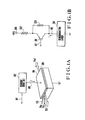
- a first embodiment of this invention comprises a semiconductor laser 104 inputted with optical input signals 106 and 107 and outputting.an optical output signal 105, and a current drive circuit 102 which varies current i supplied to the semiconductor laser 104 via a signal line 103 in accordance with a signal on an input electric signal line 101.
- the current drive cirucit 102 shown in Fig. lA comprises a transistor 201 with its base electrode connected to the signal line 101, a resistor 202 of a resistance value R 1 , having one end connected to the emitter electrode of transistor 201, a resistor 203 connected between the emitter and collector electrodes of the transistor 201 and having a resistance value of R 2 , and a power supply terminal 204 supplied with a voltage of + V EE and connected to the other end of the resistor 202.
- the transistor 201 When a sufficiently large positive voltage is applied to the base electrode of the transistor 201 via signal line 101, the transistor 201 is turned off so that a current i which is V EE /(R 1 + R 2 + r l ) will flow to the semiconductor laser 104 connected to the collector electrode of the transistor 201, where r 1 represents the internal resistance of the semiconductor laser 104.
- the transistor 201 When the base potential of transistor 201 is zero, the transistor 201 is turned on to supply a current i which is V EE /(R l + r l + r 2 ) to the semiconductor laser 104, where r 2 represents the internal resistance of the transistor 201 and R 2 » r 2 stands.
- the circuit shown in Fig. lB can supply a binary current to the semiconductor laser 104 in response to the voltage of an external signal.
- the levels of the binary current can be set to any values by suitably selecting resistance values of resistors 202 and 203.
- Fig. 2A shows the .relation between the light quantity Pout of the output optical signal 105 and the value of injection current i
- Fig. 2D shows the relation between the total quantity of the input light Pin and the quantity of output Pout when the value of the injection current i is set to i3, indicating that the Pout is maintained at a substantially constant value of Ph regardless of the value of P in .
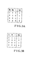
- the correspondence between the value and the logic level of each of the P in1 , P in2' i and Pout is set as follows. More specifically, the light quantity P inL corresponding to a low level of each of the P in1 and P in2 is set to satisfy a relation P inL ⁇ P l/ 2, the light quantity P inH indicative of a H(high) level of the respective P in1 and P in2 is set to satisfy realtions P 1 /2 ⁇ P inH ⁇ P 1 - P i nL and P inH ⁇ P 2 /2, the value at a L(low) level of i is set to i 1 , the value of i at a H(high) level is set to i 2 , the light quantity at the L level of Pout is set to zero, and that at the H level is set to Ph.
- Pout becomes the L level.
- P in1 is at the L level
- Pout also becomes the L level.
- P in ⁇ P 2 stands and Pout is still at the L level when both P in1 and P i n2 are at the H level.
- Fig. 3A is a truth table showing the above logical relation, in which character X represents an arbitrary level which may be either L or H level.
- the values of P in1 , P in2 , i and Pout are made to correspond to logic levels in the following manner. More particularly, the light quantity P inL at the L level of P in1 and P in2 is made to satisfy a relation P inL ⁇ P 1 /2, the light quantity P inH at the H level of P inl and P i n2 is made to satisfy a relation P 1 ⁇ P inH , the value of i at the L level is set to i 2 , the value of i at the H level is set to i 3 , the light quantity of Pout at the L level is set to 0 and that at the H level is set to Ph.
- Fig. 3B is a truth table showing this logic relation, in which character X represents an arbitrary level which may be H or L level as in the precedence.
- Fig. 4A shows the relation between the output light quantity Pout and the value of injection current i
- Figs. 4B to 4D show the relation, under the parameter of injection current i, between the light quantity Pout and the total quantity of input light Pin.
- FIG. 4B shows the relation O ⁇ i 1 ' ⁇ i 2 '.
- F ig. 4D shows the relation between P in an Pout when the injection current i is set to i 3 '. As shown, irrespective of the value of Pin, Pout is maintained substantially constant at the value Ph. Correspondence between the values of P in1 , P in2 and i of the semiconductor laser manifesting the optical bistable characteristic described above and the logic levels is set in the following manner, like a previous case of the semiconductor laser having the differential gain characteristic.
- the total light quantity P inL of P i nl and P in2 at the low level is set to satisfy a relation P inL ⁇ P 1a /2
- the total light quantity P inH at the H level is set to satisfy relations P lb /2 P inH ⁇ P 1a ⁇ - P i nL and P inH ⁇ P 2a /2
- the value of i at the L level is set to i 2 '
- the value of i at the H level is set to i 3 '
- the light quantity of Pout at the L level is set to zero
- the light quantity of Pout at the H level is set to Ph.
- the total light quantiy P inL at the L level of P in1 and P in2 is set to satisfy a relation P inL ⁇ P 1a /2
- the total light quantiy P inH at the H level of P in1 and P in2 is set to satisfy a relation P 1b ⁇ P inH '
- the value of i at the L level is set to i 2 '
- the value of i at the H level is set to i 3 '
- the light quantity of Pout at the L level is set to zero
- the light guantity of Pout at the H level is set to Ph.
- Fig. 5 shows a second embodiment of this invention which comprises an optical waveguide path 702 which receives an optical data input signal D at one end 701, an optical gate 703 having an input terminal at the other end of the optical waveguide path 702 and enabled and disabled by a gate input signal G on a signal line 708, an optical waveguide path 704 with one end connected do the output terminal of the optical gate 703, a bistable semiconductor laser 705 connected to the other end of the optical waveguide path 704, an optical waveguide path 706 with one end connected to the output terminal of the bistable semiconductor laser 705 and other end 707 emitting light, and a control circuit 709 for controlling the value of current i injected into the bistable semiconductor laser 705 via conductor 710 in accordance with a gate input signal G on the signal line 7 08.
- Figs. 6A and 6B show characteristic curves useful to explain the operation of the bistable semiconductor laser 705 shown in Fig. 5 and show the relations among current i injected into the'laser 705 via the conductor 710, the quantity of input light Pin inputted through the optical waveguide path 7.04 and the quantity of output light outputted through the optical waveguide circuit 706.
- the bistable semiconductor laser 705 manifests an hysteresis characteristic.
- Fig. 7 is a table for explaining the operation of the second embodiment of this invention shown in Fig. 5, the table showing relations among the injection current i, the quantity of input light Pin, the operating points of the bistable semiconductor laser 705 shown in Figs. 6A and 6B, and the quantity of the output light Pout.
- gate signal G is not supplied to signal line 708 shown in Fig. 5.
- the optical gate 703 is disabled, the output light quantity of the laser is zeroed irreespective of the optical data input signal D inputted to the optical gate 703.
- control circuit 709 injects current i b into the bistable semiconductor laser 705 in tht absence of the gate input signal G.
- this laser 705 operates at either one of the operating points E and F shown in F ig. 6A and the quantity of its output light Pout is maintained at Ph or zero (stored state).
- the control circuit 709 supplies an injection current i 0 to the semiconductor laser 705.
- the optical gate 703 is enabled or opened. Under these conditions, when a light data input signal D of a light quantity P 3 is applied to the bistable semiconductor laser 705 through optical waveguide paths 702, 704 and optical gate 703, the laser 705 operates at the operating point I shown in Fig. 6B so that the quantity of its light output Pout becomes Ph(set state).
- the bistable semiconductor laser 705 operates at the operating point E shown in Fig. 6A - even when the injection current i becomes i b and the quantity of light input Pin to the laser 705 becoems zero.
- optical gate 703 shown in Fig. 5 to be operated by an electric signal can be used an electronic optical switch or the first embodiment of the invention shown in Fig. 1.
- the electronic optical switch is described in detail, for example, in the Institute of Electrical and Electronics Engineers, Journal of Quantum Electronics, Oct. 1982, "Integrated optical switch matrix for single-mode fiber networks".
Landscapes
- Physics & Mathematics (AREA)
- General Physics & Mathematics (AREA)
- Optics & Photonics (AREA)
- Nonlinear Science (AREA)
- Condensed Matter Physics & Semiconductors (AREA)
- Electromagnetism (AREA)
- Semiconductor Lasers (AREA)
Applications Claiming Priority (4)
| Application Number | Priority Date | Filing Date | Title |
|---|---|---|---|
| JP163449/83 | 1983-09-06 | ||
| JP16344983A JPS6054520A (ja) | 1983-09-06 | 1983-09-06 | 光電気論理素子 |
| JP76787/84 | 1984-04-17 | ||
| JP7678784A JPH07107591B2 (ja) | 1984-04-17 | 1984-04-17 | 光情報記憶回路 |
Publications (3)
| Publication Number | Publication Date |
|---|---|
| EP0136840A2 true EP0136840A2 (de) | 1985-04-10 |
| EP0136840A3 EP0136840A3 (en) | 1986-09-17 |
| EP0136840B1 EP0136840B1 (de) | 1992-03-25 |
Family
ID=26417918
Family Applications (1)
| Application Number | Title | Priority Date | Filing Date |
|---|---|---|---|
| EP84306040A Expired EP0136840B1 (de) | 1983-09-06 | 1984-09-04 | Opto-elektronisches logisches Element |
Country Status (4)
| Country | Link |
|---|---|
| US (1) | US4802175A (de) |
| EP (1) | EP0136840B1 (de) |
| CA (1) | CA1218165A (de) |
| DE (1) | DE3485611D1 (de) |
Cited By (1)
| Publication number | Priority date | Publication date | Assignee | Title |
|---|---|---|---|---|
| EP0193819A1 (de) * | 1985-03-04 | 1986-09-10 | Hitachi, Ltd. | Einrichtung zum Verstärken und Formen von optischen Impulsen |
Families Citing this family (4)
| Publication number | Priority date | Publication date | Assignee | Title |
|---|---|---|---|---|
| US5056100A (en) * | 1990-04-19 | 1991-10-08 | California Institute Of Technology | Semiconductor laser with photon gain lever |
| US5130528A (en) * | 1991-03-01 | 1992-07-14 | International Business Machines Corporation | Opto-photo-electric switch |
| JPH06281987A (ja) * | 1993-03-26 | 1994-10-07 | Hamamatsu Photonics Kk | 光デジタル記憶装置 |
| US7133427B2 (en) * | 2003-09-19 | 2006-11-07 | Raytheon Company | Phase conjugate laser and method with improved fidelity |
Family Cites Families (6)
| Publication number | Priority date | Publication date | Assignee | Title |
|---|---|---|---|---|
| US3431437A (en) * | 1964-05-25 | 1969-03-04 | Rca Corp | Optical system for performing digital logic |
| US4038610A (en) * | 1966-11-21 | 1977-07-26 | Semiconductor Research Foundation | Luminosity control system employing semiconductor lasers |
| US3654497A (en) * | 1969-12-01 | 1972-04-04 | Bell Telephone Labor Inc | Semiconductor lasers utilizing internal saturable absorbers |
| JPS5852893A (ja) * | 1981-09-25 | 1983-03-29 | Univ Tohoku | レ−ザ機能デバイス |
| US4562569A (en) * | 1982-01-05 | 1985-12-31 | California Institute Of Technology | Tandem coupled cavity lasers with separate current control and high parasitic resistance between them for bistability and negative resistance characteristics and use thereof for optical disc readout |
| US4518934A (en) * | 1982-02-16 | 1985-05-21 | At&T Bell Laboratories | Optical bistable device |
-
1984
- 1984-09-04 DE DE8484306040T patent/DE3485611D1/de not_active Expired - Lifetime
- 1984-09-04 EP EP84306040A patent/EP0136840B1/de not_active Expired
- 1984-09-05 CA CA000462409A patent/CA1218165A/en not_active Expired
-
1986
- 1986-05-28 US US06/845,893 patent/US4802175A/en not_active Expired - Fee Related
Cited By (1)
| Publication number | Priority date | Publication date | Assignee | Title |
|---|---|---|---|---|
| EP0193819A1 (de) * | 1985-03-04 | 1986-09-10 | Hitachi, Ltd. | Einrichtung zum Verstärken und Formen von optischen Impulsen |
Also Published As
| Publication number | Publication date |
|---|---|
| EP0136840B1 (de) | 1992-03-25 |
| CA1218165A (en) | 1987-02-17 |
| US4802175A (en) | 1989-01-31 |
| DE3485611D1 (de) | 1992-04-30 |
| EP0136840A3 (en) | 1986-09-17 |
Similar Documents
| Publication | Publication Date | Title |
|---|---|---|
| US4009385A (en) | Laser control circuit | |
| US4438348A (en) | Temperature compensated avalanche photodiode optical receiver circuit | |
| EP0221710B1 (de) | Apparat zur Steuerung der Ausgangsleistung eines Lasers | |
| US4799224A (en) | Driver for a semiconductor laser | |
| JPH0529688A (ja) | 半導体レーザアレイ装置 | |
| NZ200193A (en) | Optical receiver | |
| CA1215138A (en) | Latching circuits | |
| US3970784A (en) | Transmission system | |
| EP0136840A2 (de) | Opto-elektronisches logisches Element | |
| US5216682A (en) | Laser control method and apparatus | |
| US4761060A (en) | Optical delay type flipflop and shift register using it | |
| US3462606A (en) | Photoelectric relay using positive feedback | |
| US4567384A (en) | Voltage offset producing circuit for use with a line receiver or the like | |
| US5317581A (en) | Electric field absorption light modulation driving apparatus and method having improved feature to eliminate noise from optical output | |
| EP0933872A1 (de) | Optische digitale Speichervorrichtung | |
| EP0430238A2 (de) | Empfangsschaltung mit optischer Faser zur Umsetzung eines optischen Signals in ein elektrisches Signal | |
| JPS5924561B2 (ja) | 電子制御可能な増幅要素または減衰要素の伝送量を制御する制御量発生回路 | |
| US20060140233A1 (en) | Laser driver with integrated bond options for selectable currents | |
| JPH0797194B2 (ja) | 光信号シフト回路 | |
| JPH07270730A (ja) | 光放射用光学処理装置 | |
| US5448076A (en) | Optically-coupled differential line driver generating an optical signal having at least three states | |
| US4392067A (en) | Logic select circuit | |
| US4224536A (en) | Stabilization of monolithic integrated circuit output levels | |
| SU1023658A1 (ru) | Элемент инжекционной логики со стабилизацией тока питани | |
| JPH04364790A (ja) | ファイバ形光増幅器 |
Legal Events
| Date | Code | Title | Description |
|---|---|---|---|
| PUAI | Public reference made under article 153(3) epc to a published international application that has entered the european phase |
Free format text: ORIGINAL CODE: 0009012 |
|
| 17P | Request for examination filed |
Effective date: 19840918 |
|
| AK | Designated contracting states |
Designated state(s): DE FR GB NL |
|
| PUAL | Search report despatched |
Free format text: ORIGINAL CODE: 0009013 |
|
| AK | Designated contracting states |
Kind code of ref document: A3 Designated state(s): DE FR GB NL |
|
| 17Q | First examination report despatched |
Effective date: 19880517 |
|
| GRAA | (expected) grant |
Free format text: ORIGINAL CODE: 0009210 |
|
| AK | Designated contracting states |
Kind code of ref document: B1 Designated state(s): DE FR GB NL |
|
| REF | Corresponds to: |
Ref document number: 3485611 Country of ref document: DE Date of ref document: 19920430 |
|
| ET | Fr: translation filed | ||
| PLBE | No opposition filed within time limit |
Free format text: ORIGINAL CODE: 0009261 |
|
| STAA | Information on the status of an ep patent application or granted ep patent |
Free format text: STATUS: NO OPPOSITION FILED WITHIN TIME LIMIT |
|
| 26N | No opposition filed | ||
| PGFP | Annual fee paid to national office [announced via postgrant information from national office to epo] |
Ref country code: NL Payment date: 19930930 Year of fee payment: 10 |
|
| PGFP | Annual fee paid to national office [announced via postgrant information from national office to epo] |
Ref country code: DE Payment date: 19931129 Year of fee payment: 10 |
|
| PGFP | Annual fee paid to national office [announced via postgrant information from national office to epo] |
Ref country code: GB Payment date: 19940831 Year of fee payment: 11 |
|
| PG25 | Lapsed in a contracting state [announced via postgrant information from national office to epo] |
Ref country code: NL Effective date: 19950401 |
|
| NLV4 | Nl: lapsed or anulled due to non-payment of the annual fee | ||
| PG25 | Lapsed in a contracting state [announced via postgrant information from national office to epo] |
Ref country code: DE Effective date: 19950601 |
|
| PG25 | Lapsed in a contracting state [announced via postgrant information from national office to epo] |
Ref country code: GB Effective date: 19950904 |
|
| GBPC | Gb: european patent ceased through non-payment of renewal fee |
Effective date: 19950904 |
|
| PGFP | Annual fee paid to national office [announced via postgrant information from national office to epo] |
Ref country code: FR Payment date: 19980909 Year of fee payment: 15 |
|
| PG25 | Lapsed in a contracting state [announced via postgrant information from national office to epo] |
Ref country code: FR Free format text: LAPSE BECAUSE OF NON-PAYMENT OF DUE FEES Effective date: 20000531 |
|
| REG | Reference to a national code |
Ref country code: FR Ref legal event code: ST |