EP0139764B1 - Procede de fabrication des dispositifs integres a film mince - Google Patents
Procede de fabrication des dispositifs integres a film mince Download PDFInfo
- Publication number
- EP0139764B1 EP0139764B1 EP84901397A EP84901397A EP0139764B1 EP 0139764 B1 EP0139764 B1 EP 0139764B1 EP 84901397 A EP84901397 A EP 84901397A EP 84901397 A EP84901397 A EP 84901397A EP 0139764 B1 EP0139764 B1 EP 0139764B1
- Authority
- EP
- European Patent Office
- Prior art keywords
- thin film
- film
- sputtering
- composite oxide
- tantalum
- Prior art date
- Legal status (The legal status is an assumption and is not a legal conclusion. Google has not performed a legal analysis and makes no representation as to the accuracy of the status listed.)
- Expired
Links
Images




Classifications
-
- H—ELECTRICITY
- H10—SEMICONDUCTOR DEVICES; ELECTRIC SOLID-STATE DEVICES NOT OTHERWISE PROVIDED FOR
- H10D—INORGANIC ELECTRIC SEMICONDUCTOR DEVICES
- H10D64/00—Electrodes of devices having potential barriers
- H10D64/60—Electrodes characterised by their materials
- H10D64/66—Electrodes having a conductor capacitively coupled to a semiconductor by an insulator, e.g. MIS electrodes
- H10D64/68—Electrodes having a conductor capacitively coupled to a semiconductor by an insulator, e.g. MIS electrodes characterised by the insulator, e.g. by the gate insulator
- H10D64/691—Electrodes having a conductor capacitively coupled to a semiconductor by an insulator, e.g. MIS electrodes characterised by the insulator, e.g. by the gate insulator comprising metallic compounds, e.g. metal oxides or metal silicates
-
- H—ELECTRICITY
- H01—ELECTRIC ELEMENTS
- H01B—CABLES; CONDUCTORS; INSULATORS; SELECTION OF MATERIALS FOR THEIR CONDUCTIVE, INSULATING OR DIELECTRIC PROPERTIES
- H01B3/00—Insulators or insulating bodies characterised by the insulating materials; Selection of materials for their insulating or dielectric properties
- H01B3/02—Insulators or insulating bodies characterised by the insulating materials; Selection of materials for their insulating or dielectric properties mainly consisting of inorganic substances
- H01B3/12—Insulators or insulating bodies characterised by the insulating materials; Selection of materials for their insulating or dielectric properties mainly consisting of inorganic substances ceramics
-
- H—ELECTRICITY
- H01—ELECTRIC ELEMENTS
- H01G—CAPACITORS; CAPACITORS, RECTIFIERS, DETECTORS, SWITCHING DEVICES, LIGHT-SENSITIVE OR TEMPERATURE-SENSITIVE DEVICES OF THE ELECTROLYTIC TYPE
- H01G4/00—Fixed capacitors; Processes of their manufacture
- H01G4/002—Details
- H01G4/018—Dielectrics
- H01G4/06—Solid dielectrics
- H01G4/08—Inorganic dielectrics
- H01G4/10—Metal-oxide dielectrics
-
- H—ELECTRICITY
- H05—ELECTRIC TECHNIQUES NOT OTHERWISE PROVIDED FOR
- H05B—ELECTRIC HEATING; ELECTRIC LIGHT SOURCES NOT OTHERWISE PROVIDED FOR; CIRCUIT ARRANGEMENTS FOR ELECTRIC LIGHT SOURCES, IN GENERAL
- H05B33/00—Electroluminescent light sources
- H05B33/12—Light sources with substantially two-dimensional [2D] radiating surfaces
- H05B33/22—Light sources with substantially two-dimensional [2D] radiating surfaces characterised by the chemical or physical composition or the arrangement of auxiliary dielectric or reflective layers
-
- H—ELECTRICITY
- H10—SEMICONDUCTOR DEVICES; ELECTRIC SOLID-STATE DEVICES NOT OTHERWISE PROVIDED FOR
- H10D—INORGANIC ELECTRIC SEMICONDUCTOR DEVICES
- H10D30/00—Field-effect transistors [FET]
- H10D30/60—Insulated-gate field-effect transistors [IGFET]
- H10D30/67—Thin-film transistors [TFT]
- H10D30/6729—Thin-film transistors [TFT] characterised by the electrodes
- H10D30/6737—Thin-film transistors [TFT] characterised by the electrodes characterised by the electrode materials
- H10D30/6739—Conductor-insulator-semiconductor electrodes
-
- H—ELECTRICITY
- H10—SEMICONDUCTOR DEVICES; ELECTRIC SOLID-STATE DEVICES NOT OTHERWISE PROVIDED FOR
- H10D—INORGANIC ELECTRIC SEMICONDUCTOR DEVICES
- H10D30/00—Field-effect transistors [FET]
- H10D30/60—Insulated-gate field-effect transistors [IGFET]
- H10D30/67—Thin-film transistors [TFT]
- H10D30/674—Thin-film transistors [TFT] characterised by the active materials
- H10D30/675—Group III-V materials, Group II-VI materials, Group IV-VI materials, selenium or tellurium
-
- H—ELECTRICITY
- H10—SEMICONDUCTOR DEVICES; ELECTRIC SOLID-STATE DEVICES NOT OTHERWISE PROVIDED FOR
- H10D—INORGANIC ELECTRIC SEMICONDUCTOR DEVICES
- H10D86/00—Integrated devices formed in or on insulating or conducting substrates, e.g. formed in silicon-on-insulator [SOI] substrates or on stainless steel or glass substrates
- H10D86/80—Integrated devices formed in or on insulating or conducting substrates, e.g. formed in silicon-on-insulator [SOI] substrates or on stainless steel or glass substrates characterised by multiple passive components, e.g. resistors, capacitors or inductors
-
- H—ELECTRICITY
- H10—SEMICONDUCTOR DEVICES; ELECTRIC SOLID-STATE DEVICES NOT OTHERWISE PROVIDED FOR
- H10P—GENERIC PROCESSES OR APPARATUS FOR THE MANUFACTURE OR TREATMENT OF DEVICES COVERED BY CLASS H10
- H10P14/00—Formation of materials, e.g. in the shape of layers or pillars
- H10P14/60—Formation of materials, e.g. in the shape of layers or pillars of insulating materials
- H10P14/63—Formation of materials, e.g. in the shape of layers or pillars of insulating materials characterised by the formation processes
- H10P14/6302—Non-deposition formation processes
- H10P14/6304—Formation by oxidation, e.g. oxidation of the substrate
- H10P14/6314—Formation by oxidation, e.g. oxidation of the substrate of a metallic layer
-
- H—ELECTRICITY
- H10—SEMICONDUCTOR DEVICES; ELECTRIC SOLID-STATE DEVICES NOT OTHERWISE PROVIDED FOR
- H10P—GENERIC PROCESSES OR APPARATUS FOR THE MANUFACTURE OR TREATMENT OF DEVICES COVERED BY CLASS H10
- H10P14/00—Formation of materials, e.g. in the shape of layers or pillars
- H10P14/60—Formation of materials, e.g. in the shape of layers or pillars of insulating materials
- H10P14/63—Formation of materials, e.g. in the shape of layers or pillars of insulating materials characterised by the formation processes
- H10P14/6326—Deposition processes
- H10P14/6328—Deposition from the gas or vapour phase
- H10P14/6329—Deposition from the gas or vapour phase using physical ablation of a target, e.g. physical vapour deposition or pulsed laser deposition
-
- H—ELECTRICITY
- H10—SEMICONDUCTOR DEVICES; ELECTRIC SOLID-STATE DEVICES NOT OTHERWISE PROVIDED FOR
- H10P—GENERIC PROCESSES OR APPARATUS FOR THE MANUFACTURE OR TREATMENT OF DEVICES COVERED BY CLASS H10
- H10P14/00—Formation of materials, e.g. in the shape of layers or pillars
- H10P14/60—Formation of materials, e.g. in the shape of layers or pillars of insulating materials
- H10P14/69—Inorganic materials
- H10P14/692—Inorganic materials composed of oxides, glassy oxides or oxide-based glasses
- H10P14/6938—Inorganic materials composed of oxides, glassy oxides or oxide-based glasses the material containing at least one metal element, e.g. metal oxides, metal oxynitrides or metal oxycarbides
- H10P14/6939—Inorganic materials composed of oxides, glassy oxides or oxide-based glasses the material containing at least one metal element, e.g. metal oxides, metal oxynitrides or metal oxycarbides characterised by the metal
- H10P14/69391—Inorganic materials composed of oxides, glassy oxides or oxide-based glasses the material containing at least one metal element, e.g. metal oxides, metal oxynitrides or metal oxycarbides characterised by the metal the material containing aluminium, e.g. Al2O3
-
- H—ELECTRICITY
- H10—SEMICONDUCTOR DEVICES; ELECTRIC SOLID-STATE DEVICES NOT OTHERWISE PROVIDED FOR
- H10P—GENERIC PROCESSES OR APPARATUS FOR THE MANUFACTURE OR TREATMENT OF DEVICES COVERED BY CLASS H10
- H10P14/00—Formation of materials, e.g. in the shape of layers or pillars
- H10P14/60—Formation of materials, e.g. in the shape of layers or pillars of insulating materials
- H10P14/69—Inorganic materials
- H10P14/692—Inorganic materials composed of oxides, glassy oxides or oxide-based glasses
- H10P14/6938—Inorganic materials composed of oxides, glassy oxides or oxide-based glasses the material containing at least one metal element, e.g. metal oxides, metal oxynitrides or metal oxycarbides
- H10P14/6939—Inorganic materials composed of oxides, glassy oxides or oxide-based glasses the material containing at least one metal element, e.g. metal oxides, metal oxynitrides or metal oxycarbides characterised by the metal
- H10P14/69393—Inorganic materials composed of oxides, glassy oxides or oxide-based glasses the material containing at least one metal element, e.g. metal oxides, metal oxynitrides or metal oxycarbides characterised by the metal the material containing tantalum, e.g. Ta2O5
Definitions
- This invention relates to a method of manufacturing thin film integrated devices wherein a plurality of thin film condensors, thin film transistors, and thin film light emitting elements, etc. are integrated.
- thin oxide film elements are used as the thin oxide film elements in thin film integrated devices. These oxide films often play a basic role in the function of the device. The characteristics of the oxide films themselves influence the qualities of those of the respective thin film elements in the devices.
- a known method of forming a hybrid integrated circuit is described in Thin Solid Films Volume 56 No. 3 (1st February 1979) page 357 to 362 and Thin Solid Films Volume 109 (1983) page 339 to 343.
- a method of manufacture of integrated thin film resistors and condensors is disclosed, which result in a thin film alloy of tantalum and aluminum.
- the tantalum and aluminum film is formed by a sputtering technique whilst doping with oxygen and nitrogen.
- This forms a thin film layer which is subsequently partially oxidised by an anodic oxidation process to produce a composite oxide layer.
- This anodic oxidation process requires the provision of current paths for the anodic formation.
- the above-mentioned thin film of tantalum- aluminium alloy has a high resistivity.
- the dielectric loss (tan 6) becomes large at high frequencies and the usable frequency band is reduced.
- the breakdown field intensity (Eb) of the condenser becomes small.
- tantalum oxide formed by the sputtering method has many pinholes and hence the leakage current is large. Since the breakdown field intensity Eb is also low (about 1.5x10 6 V. cm-1), the film thickness should be made large. This makes it difficult to obtain a large capacitance element. Even aluminum oxide formed by the sputtering method has a small dielectric constant (e,) and cannot form a large capacitance element.
- Thin film transistors have been intensively studied as a driver for liquid crystals and EL display devices, etc., in which an on-off ratio of current is desired.
- the gate oxide film should have a large dielectric constant (s,) to increase the mutual conductance (gm) and a small leakage current to decrease the off-current.
- s, dielectric constant
- Gm mutual conductance
- gm mutual conductance
- gm mutual conductance
- the characteristics of the interface between the semiconductor layer and the gate oxide film are good.
- the thin film light emitting element is represented by a thin film EL (electroluminescence) element using a ZnS:Mn emission layer.
- the field intensity for obtaining the EL emission is high, about 10 6 Vcm-'.
- An EL thin film element with a high brightness is desired, in which the electric field is applied efficiently to the emission layer and which has a low threshold voltage for light emission and can operate with a low voltage.
- the oxide film provided on the both sides or on one side of the emission layer has a large dielectric constant (er), a high breakdown voltage and a low leakage current.
- An EL display device of matrix type is constituted with thin film EL elements, thin film transistors and thin film condensers, etc. Therefore, in order to increase the reliability, the oxide films used in these elements should have the above-mentioned characteristics. This is also the case with a liquid crystal display device of matrix type.
- a method of manufacturing a thin film integrated device wherein at least one thin film element is supported on an insulating substrate including the step of:- forming a composite oxide thin film, comprising major con- stitutents of at least tantalum and aluminum which are oxidised, by means of sputtering a composite target of tantalum or tantalum oxide and aluminum or aluminum oxide as major constituents; the method being characterised in that the sputtering is r.f. sputtering and the sputtering parameters are such that the resultant film is completely oxidised by sputtering only so that a subsequent step of anodic oxidation is not required.
- the invention thus provides a simple method of manufacturing a thin film integrated device using a sputtered composite oxide thin film of aluminum and tantalum as major constituents, which has a large dielectric constant (er), a large breakdown field (Eb) and a small leakage current.
- the sputtered composite oxide thin film produced according to this invention is used as a dielectric thin film constituting a thin film condenser, a thin film condenser having a large capacitance and a stable dielectric characteristic can be obtained.
- the sputtered composite oxide thin film is used as a gate insulation film between the semiconductor layer and the gate electrode which constitute a thin film transistor, a characteristic with a large gm and a small leakage current can be obtained. Therefore, a thin film transistor with an on-off ratio of current can be obtained.
- the semiconductor layer is cadmium selenide (CdSe)
- the interface characteristic is good and the transistor characteristic is stable with little temporal variation.
- the sputtered composite oxide thin film produced according to this invention is provided on both sides or on one side of a phosphorthin film constituting a thin film light emitting element, a high electric field can be applied efficiently to the phosphor thin film.
- a thin film light emitting element having a high brightness and capable of being driven with a low voltage can be obtained.
- this phosphor thin film is a light emission layer composed of zinc sulfide containing a luminescent activator as a major constituent, one can obtain a thin film light emitting element which has a specifically high brightness by applying alternating voltages but is hard to cause breakdown.
- thin film light emitting elements with various light colors can be constituted.
- a display cell for one picture element comprises a switching transistor, a storage condenser whose one electrode is connected to the source electrode of the switching transistor, and a power transistor whose gate electrode is connected to the source electrode of the switching transistor and whose source electrode is connected to the other electrode of the storage condenser; if at least one layer of the above produced sputtered composite oxide thin film is provided, it can be used as a gate oxide film for the above-mentioned switching transistor and power transistor or as a dielectric thin film of the storage condenser. For the same reason as the above-mentioned one, the characteristic of each thin film element can be improved and as a whole a stable thin film integrated device with a high reliability can be obtained.
- an electrode 2 is provided on one surface of a supporting substrate wherein an insulation film is formed on the surface of an insulator such as glass or an electric conductor such as metal.
- This electrode 2 is aluminum having a film thickness of the order of 100 nm and formed by a vacuum evaporation method, etc.
- a sputtered composite oxide thin film with a film thickness of the order of 500 nm is formed of tantalum and aluminum as major components as a dielectric thin film 3.
- an electrode 4 is provided on this dielectric thin film 3.
- This electrode 4 is an aluminum layer with a film thickness of the order of 100 nm similar to the electrode 2, and is formed by a vacuum evaporation method, etc.
- the dielectric thin film 3 was formed by the reactive sputtering of a composite target comprising tantalum and aluminum plates in an inert gas containing oxygen. Ratio of oxygen was 25%, and a radio frequency magnetron sputtering was done in an atmosphere of 4.Ox10-3 Torr. (5.3 10-' Pa). According to this method, a sputtered composite oxide thin film of any component-combination ratio can be formed with a good reproducibility by varying the area ratio of tantalum and aluminum in the composite target.
- Figure 2 shows the relations of the dielectric constant (sr) and the dielectric loss (tan 6) against the ratio of tantalum atoms (the value of where the number of tantalum atoms is denoted by x and that of aluminum atoms by y) of the sputtered composite oxide thin film.
- the ratio of tantalum atoms was measured by EDX. As apparent from Figure 2, it is possible to select er freely from 7 to 25. By an appropriate choice of the ratio of the number of tantalum atoms, a sputtered composite oxide thin film with a large er can be obtained.
- tan 6 is about 0.2% and varies scarcely. The film has an excellent dielectric characteristic.
- Figure 3 shows the relation between the leakage current per unit capacitance and the applied voltage when the ratio of the number of tantalum atoms in the sputtered composite oxide thin film is varied.
- Solid lines a, b, c, d in the figure denote measured results when the ratio of the number of tantalum atoms is 1.00, 0.84, 0.37, 0.00 respectively.
- the leakage current per unit capacitance of the composite oxide thin films (b, c) is extremely smaller in comparison with that of tantalum oxide (a).
- the leakage current per unit capacitance becomes smaller than that (d) of aluminum oxide only if the applied voltage is below 60 V because the dielectric constant (er) is larger.
- FIG. 4 shows the relation of the breakdown field intensity (Eb) and the product of Eb and the dielectric constant (sr), (Eb - sr), against the ratio of the number of tantalum atoms in the sputtered composite oxide thin film.
- the material for the underlying electrode can be selected freely.
- the material for the underlying electrode can be selected freely.
- the dielectric loss (tan 6) even at high frequencies thereby to widen the practical frequency band.
- the film since the sputtered composite oxide thin film in the neighborhood of the interface of the underlying electrode is perfectly oxidized, the film has characteristics: breakdown field intensity (Eb) is large and the leakage current is small.
- the sputtered composite oxide thin film in this invention has a strong force of attachment with electrode materials (ITO, aluminum, etc.) and an excellent water-proof property.
- the leakage current of this sputtered composite oxide thin film was measured by varying the annealing temperature.
- the leakage current became constant to a value less than one tenth of the value before annealing, if the annealing was done with a temperature above 300°C.
- Figure 5 shows another embodiment where this sputtered composite oxide thin film is applied to a thin film transistor.
- a gate electrode 6 of aluminum having a film of the order of 100 nm was formed and thereon a composite oxide thin film with a film thickness of the order of 500 nm was formed as a gate insulation film 7 by the radio frequency magnetron sputtering method.
- a semiconductor layer 8 and thereon source and drain electrodes of aluminum 9 and 10 with a film thickness of the order of 10 nm were formed. Since the gate insulation film of this thin film transistor is the sputtered composite oxide thin film having the characteristics as mentioned above, the mutual conductance (gm) becomes larger than in the prior art. Therefore, the on- current becomes large while the gate leakage current becomes small, so that a characteristic with a small off-current was obtained. The on-off ratio of current became above 10000 when the gate voltage was varied from 0 V to 20 V.
- CdSe cadmium selenide
- the characteristic of the interface between CdSe and the sputtered composite oxide thin film was good.
- a stable thin film transistor with a small temporal variation of drain current as shown in Figure 6 was obtained.
- both the gate voltage and the drain voltage were kept constant at 10 V.
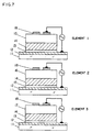
- Figure 7 shows an embodiment where this sputtered composite oxide thin film is used as a thin film light emitting element.
- a transparent electrode 12 of indium tin oxide (ITO) with a film thickness of the order of 100 nm and thereon an insulation layer 13 of Y 2 0 3 with a film thickness of the order of 50 nm were evaporated by an electron beam.
- a phosphor layer 14 of ZnS: Mn with a film thickness of the order of 200 nm was evaporated by an electron beam.
- the element was divided into three elements. On a first element 1 and a second element 2 of them, an insulating layer 15 of tantalum oxide and an insulating layer 16 of aluminum oxide having a film thickness of the order of 300 nm were formed by the radio frequency magnetron sputtering method, respectively. On the other hand, on the third element 3 an insulating layer 17 of the composite oxide film of this invention with the ratio of the number of tantalum atoms 0.7 was formed by the radio frequency magnetron sputtering method. Finally, aluminum electrodes 18 for light reflection with a film thickness of the order of 100 nm were vacuum-evaporated.
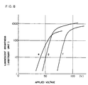
- the above three elements were driven by applying a sinusoidal voltage with a frequency of 5 KHz.
- the luminescence brightness became as shown in Figure 8.
- e, f, g correspond to the element 1, element 2, element 3 respectively.
- the figure shows that, in the case of tantatum oxide of the element 1, the luminescence brightness cannot be increased. This is because the breakdown voltage (Eb) is small and hence no high electric field can be applied.
- the driving voltage In the case of the aluminum oxide of element 2, the driving voltage is high. It is seen that in the case of the element 3 with the sputtered composite oxide thin film, since the driving voltage is low and the breakdown voltage is increased, a high brightness is obtainable.
- the luminescent activator is Mn
- a similar effect was obtained if it is at least a kind selected from a group of Cu, Ag, Al, Tb, Dy, Er, Pr, Sm, Ho; Tm and their halides.
- Figure 9(a) shows the circuit diagram of one picture-element for a case where the thin film integrated device produced according to the present invention is an EL display device of matrix type.
- one picture element is constituted with a switching transistor T 1 , a storage condenser Cs, a power transistor T 2 and an EL element. Scanning lines X,, X I+1 ... and signal lines Y j , Y j+1 , ... intersect with one another.
- the sputtered composite oxide thin film formed simultaneously with the formation of the above-mentioned thin film element can be used as an electric insulating layer between the thin films of X electrodes and Y electrodes.
- Figure 9(b) shows a cross-section of one embodiment of the above-mentioned EL display device of matrix type.
- EL layer 20 is provided on an insulating substrate 19 of glass, etc. by the above-mentioned method.
- aluminum layers with a film thickness of the order of 100 nm are formed as the gate electrode 21 of a switching transistor T l , as one side electrode of a storage condenser Cs and gate electrode 22 of a power transistor T 2 and as the light reflecting electrode 23 of the EL layer by using the vacuum evaporation method and the photolithographic technique.
- a composite oxide thin film produced according to the present invention with a film thickness of the order of 500 nm is provided by the radio frequency magnetron sputtering method. Patterning is performed by using the photolithographic technique to form a gate insulating film 24 of T, and a layer 25 which is a dielectric thin film layer of Cs and the gate insulating film of T 2 . On these films, semiconductor layers 26, 27 of T I ,T 2 are provided. Finally provided are electrode layers 28 of aluminum with a film thickness of the order of 100 nm, which are the source and drain electrodes of T l , T 2 , and the one side electrode of C s .
- this invention uses an oxide thin film of tantalum and aluminum as major components formed by the sputtering method as a composite oxide thin film.
- a thin-film integrated device can be realized wherein one kind or various kinds of thin film elements such as large capacitance thin film condensers, thin film transistors with a large on/off ratio and thin film light emitting elements with a high luminescence brightness, etc. are integrated. Since the operation characteristic and reliability of the thin-film integrated device can be improved largely, the practical value is large.
Landscapes
- Chemical & Material Sciences (AREA)
- Engineering & Computer Science (AREA)
- Inorganic Chemistry (AREA)
- Power Engineering (AREA)
- Manufacturing & Machinery (AREA)
- Microelectronics & Electronic Packaging (AREA)
- Ceramic Engineering (AREA)
- Electroluminescent Light Sources (AREA)
- Formation Of Insulating Films (AREA)
- Semiconductor Integrated Circuits (AREA)
Abstract
Claims (6)
Applications Claiming Priority (4)
| Application Number | Priority Date | Filing Date | Title |
|---|---|---|---|
| JP58057552A JPS59182572A (ja) | 1983-03-31 | 1983-03-31 | 薄膜トランジスタとその製造方法 |
| JP57552/83 | 1983-03-31 | ||
| JP58098343A JPS59224098A (ja) | 1983-06-02 | 1983-06-02 | 薄膜発光素子 |
| JP98343/83 | 1983-06-02 |
Publications (3)
| Publication Number | Publication Date |
|---|---|
| EP0139764A1 EP0139764A1 (fr) | 1985-05-08 |
| EP0139764A4 EP0139764A4 (fr) | 1986-11-05 |
| EP0139764B1 true EP0139764B1 (fr) | 1989-10-18 |
Family
ID=26398611
Family Applications (1)
| Application Number | Title | Priority Date | Filing Date |
|---|---|---|---|
| EP84901397A Expired EP0139764B1 (fr) | 1983-03-31 | 1984-03-29 | Procede de fabrication des dispositifs integres a film mince |
Country Status (4)
| Country | Link |
|---|---|
| US (1) | US4602192A (fr) |
| EP (1) | EP0139764B1 (fr) |
| DE (1) | DE3480243D1 (fr) |
| WO (1) | WO1984003992A1 (fr) |
Families Citing this family (43)
| Publication number | Priority date | Publication date | Assignee | Title |
|---|---|---|---|---|
| US4890150A (en) * | 1985-12-05 | 1989-12-26 | North American Philips Corporation | Dielectric passivation |
| US4803536A (en) * | 1986-10-24 | 1989-02-07 | Xerox Corporation | Electrostatic discharge protection network for large area transducer arrays |
| JPH0240891A (ja) * | 1988-07-29 | 1990-02-09 | Toshiba Corp | 薄膜型エレクトロルミネッセンス表示素子 |
| JP2952887B2 (ja) * | 1989-05-20 | 1999-09-27 | 富士通株式会社 | 半導体装置およびその製造方法 |
| JPH0758635B2 (ja) * | 1989-11-24 | 1995-06-21 | 富士ゼロックス株式会社 | El駆動回路 |
| JPH0766246B2 (ja) * | 1989-12-15 | 1995-07-19 | 富士ゼロックス株式会社 | El駆動回路 |
| JP2794678B2 (ja) * | 1991-08-26 | 1998-09-10 | 株式会社 半導体エネルギー研究所 | 絶縁ゲイト型半導体装置およびその作製方法 |
| JP2873632B2 (ja) | 1991-03-15 | 1999-03-24 | 株式会社半導体エネルギー研究所 | 半導体装置 |
| US6713783B1 (en) | 1991-03-15 | 2004-03-30 | Semiconductor Energy Laboratory Co., Ltd. | Compensating electro-optical device including thin film transistors |
| US5177406A (en) * | 1991-04-29 | 1993-01-05 | General Motors Corporation | Active matrix vacuum fluorescent display with compensation for variable phosphor efficiency |
| US7071910B1 (en) | 1991-10-16 | 2006-07-04 | Semiconductor Energy Laboratory Co., Ltd. | Electrooptical device and method of driving and manufacturing the same |
| JP2784615B2 (ja) * | 1991-10-16 | 1998-08-06 | 株式会社半導体エネルギー研究所 | 電気光学表示装置およびその駆動方法 |
| US7253440B1 (en) * | 1991-10-16 | 2007-08-07 | Semiconductor Energy Laboratory Co., Ltd. | Semiconductor device having at least first and second thin film transistors |
| US6759680B1 (en) | 1991-10-16 | 2004-07-06 | Semiconductor Energy Laboratory Co., Ltd. | Display device having thin film transistors |
| JPH05315608A (ja) * | 1992-05-13 | 1993-11-26 | Tadahiro Omi | 半導体装置 |
| US5302966A (en) * | 1992-06-02 | 1994-04-12 | David Sarnoff Research Center, Inc. | Active matrix electroluminescent display and method of operation |
| US5587329A (en) * | 1994-08-24 | 1996-12-24 | David Sarnoff Research Center, Inc. | Method for fabricating a switching transistor having a capacitive network proximate a drift region |
| JPH08129360A (ja) * | 1994-10-31 | 1996-05-21 | Tdk Corp | エレクトロルミネセンス表示装置 |
| US5550066A (en) * | 1994-12-14 | 1996-08-27 | Eastman Kodak Company | Method of fabricating a TFT-EL pixel |
| US5640067A (en) * | 1995-03-24 | 1997-06-17 | Tdk Corporation | Thin film transistor, organic electroluminescence display device and manufacturing method of the same |
| US6853083B1 (en) * | 1995-03-24 | 2005-02-08 | Semiconductor Energy Laboratory Co., Ltd. | Thin film transfer, organic electroluminescence display device and manufacturing method of the same |
| US5952789A (en) * | 1997-04-14 | 1999-09-14 | Sarnoff Corporation | Active matrix organic light emitting diode (amoled) display pixel structure and data load/illuminate circuit therefor |
| US6538554B1 (en) | 1997-04-18 | 2003-03-25 | Berger, Ii Robert E. | Resistors formed of aluminum-titanium alloys |
| US6072278A (en) * | 1997-08-06 | 2000-06-06 | Alliedsignal Inc. | High capacitance pixel for electronic displays |
| US6060406A (en) * | 1998-05-28 | 2000-05-09 | Lucent Technologies Inc. | MOS transistors with improved gate dielectrics |
| US8853696B1 (en) * | 1999-06-04 | 2014-10-07 | Semiconductor Energy Laboratory Co., Ltd. | Electro-optical device and electronic device |
| US6552403B1 (en) * | 1999-11-05 | 2003-04-22 | North Carolina State University | Binary non-crystalline oxide analogs of silicon dioxide for use in gate dielectrics |
| JP4827294B2 (ja) * | 1999-11-29 | 2011-11-30 | 株式会社半導体エネルギー研究所 | 成膜装置及び発光装置の作製方法 |
| TW490714B (en) * | 1999-12-27 | 2002-06-11 | Semiconductor Energy Lab | Film formation apparatus and method for forming a film |
| US6307322B1 (en) | 1999-12-28 | 2001-10-23 | Sarnoff Corporation | Thin-film transistor circuitry with reduced sensitivity to variance in transistor threshold voltage |
| US20020011205A1 (en) | 2000-05-02 | 2002-01-31 | Shunpei Yamazaki | Film-forming apparatus, method of cleaning the same, and method of manufacturing a light-emitting device |
| US7517551B2 (en) * | 2000-05-12 | 2009-04-14 | Semiconductor Energy Laboratory Co., Ltd. | Method of manufacturing a light-emitting device |
| JPWO2002075710A1 (ja) * | 2001-03-21 | 2004-07-08 | キヤノン株式会社 | アクティブマトリクス型発光素子の駆動回路 |
| TWI266999B (en) * | 2001-10-10 | 2006-11-21 | Semiconductor Energy Lab | Production system and production method |
| KR100538144B1 (ko) * | 2002-01-29 | 2005-12-22 | (주)그라쎌 | 발광소자 구동회로 및 이를 채용한 매트릭스형 디스플레이패널 |
| SG113448A1 (en) * | 2002-02-25 | 2005-08-29 | Semiconductor Energy Lab | Fabrication system and a fabrication method of a light emitting device |
| EP1369499A3 (fr) * | 2002-04-15 | 2004-10-20 | Semiconductor Energy Laboratory Co., Ltd. | Méthode et appareillage pour fabriquer un dispositif émetteur de lumière |
| US20030221620A1 (en) * | 2002-06-03 | 2003-12-04 | Semiconductor Energy Laboratory Co., Ltd. | Vapor deposition device |
| JP2004047503A (ja) * | 2002-07-08 | 2004-02-12 | Fujitsu Ltd | 半導体装置及びその製造方法 |
| AU2003263609A1 (en) | 2002-09-20 | 2004-04-08 | Semiconductor Energy Laboratory Co., Ltd. | Fabrication system and manufacturing method of light emitting device |
| JP4216707B2 (ja) * | 2003-12-25 | 2009-01-28 | 株式会社東芝 | 半導体装置の製造方法 |
| US7291522B2 (en) | 2004-10-28 | 2007-11-06 | Hewlett-Packard Development Company, L.P. | Semiconductor devices and methods of making |
| WO2014009601A1 (fr) * | 2012-06-21 | 2014-01-16 | Beneq Oy | Élément d'affichage électroluminescent à couche mince transparent inorganique et son procédé de fabrication |
Family Cites Families (15)
| Publication number | Priority date | Publication date | Assignee | Title |
|---|---|---|---|---|
| GB1067831A (en) * | 1964-03-11 | 1967-05-03 | Ultra Electronics Ltd | Improvements in thin film circuits |
| US3556966A (en) * | 1968-01-19 | 1971-01-19 | Rca Corp | Plasma anodizing aluminium coatings on a semiconductor |
| SE348216B (fr) * | 1968-08-12 | 1972-08-28 | Western Electric Co | |
| US3663870A (en) * | 1968-11-13 | 1972-05-16 | Tokyo Shibaura Electric Co | Semiconductor device passivated with rare earth oxide layer |
| DE1923265B2 (de) * | 1969-05-07 | 1972-06-22 | Licentia Patent Verwaltungs GmbH, 6000 Frankfurt | Verfahren zum herstellen eines feldeffekttransistors mit isolierter steuerelektrode |
| US3878549A (en) * | 1970-10-27 | 1975-04-15 | Shumpei Yamazaki | Semiconductor memories |
| JPS4954850A (fr) * | 1972-09-28 | 1974-05-28 | ||
| GB1424980A (en) * | 1973-06-20 | 1976-02-11 | Siemens Ag | Thin-film electrical circuits |
| US3997411A (en) * | 1973-06-20 | 1976-12-14 | Siemens Aktiengesellschaft | Method for the production of a thin film electric circuit |
| JPS5310283A (en) * | 1976-07-15 | 1978-01-30 | Matsushita Electric Ind Co Ltd | 54)mos type semiconductor integrated circuit |
| GB1565551A (en) * | 1977-01-06 | 1980-04-23 | Westinghouse Electric Corp | Thin film transistor |
| JPS5824915B2 (ja) * | 1977-10-11 | 1983-05-24 | シャープ株式会社 | 薄膜el素子 |
| JPS5852284Y2 (ja) * | 1980-02-08 | 1983-11-29 | 富士通株式会社 | スパッタリング用タ−ゲット |
| JPS6040160B2 (ja) * | 1980-08-28 | 1985-09-09 | 松下電器産業株式会社 | 電場発光素子 |
| JPS5823191A (ja) * | 1981-07-31 | 1983-02-10 | シャープ株式会社 | 薄膜el素子 |
-
1984
- 1984-03-29 DE DE8484901397T patent/DE3480243D1/de not_active Expired
- 1984-03-29 WO PCT/JP1984/000145 patent/WO1984003992A1/fr not_active Ceased
- 1984-03-29 EP EP84901397A patent/EP0139764B1/fr not_active Expired
- 1984-03-29 US US06/678,547 patent/US4602192A/en not_active Expired - Lifetime
Also Published As
| Publication number | Publication date |
|---|---|
| DE3480243D1 (en) | 1989-11-23 |
| EP0139764A1 (fr) | 1985-05-08 |
| US4602192A (en) | 1986-07-22 |
| EP0139764A4 (fr) | 1986-11-05 |
| WO1984003992A1 (fr) | 1984-10-11 |
Similar Documents
| Publication | Publication Date | Title |
|---|---|---|
| EP0139764B1 (fr) | Procede de fabrication des dispositifs integres a film mince | |
| US4686110A (en) | Method for preparing a thin-film electroluminescent display panel comprising a thin metal oxide layer and thick dielectric layer | |
| US4482841A (en) | Composite dielectrics for low voltage electroluminescent displays | |
| EP0111568A1 (fr) | Dispositif electroluminescent a champ electrique a film mince | |
| US6036823A (en) | Dielectric thin film and thin-film EL device using same | |
| US4594282A (en) | Layer structure of thin-film electroluminescent display panel | |
| US5164799A (en) | Thin-film electroluminescent device having a dual dielectric structure | |
| US5721562A (en) | Electroluminescent display device including a columnar crystal structure insulating film | |
| JPH054797B2 (fr) | ||
| JPS5829880A (ja) | 電場発光素子 | |
| EP0450077A1 (fr) | Element electroluminescent a film mince et procede de fabrication de cet element | |
| KR100283283B1 (ko) | 평탄한 계면을 갖는 전계발광 소자 및 제조방법 | |
| JP2813259B2 (ja) | 薄膜誘電体 | |
| JPH0544157B2 (fr) | ||
| JPS61151996A (ja) | 薄膜エレクトロルミネセンス素子およびその製造方法 | |
| JPH056793A (ja) | 薄膜el素子の製造方法 | |
| Ohwaki et al. | Stacked Insulator Structure Thin‐Film Electroluminescent Display Devices | |
| KR100235832B1 (ko) | 박막 전계 발광 소자 | |
| JPH0124358B2 (fr) | ||
| JPH03112089A (ja) | 薄膜el素子 | |
| JPH0740515B2 (ja) | 薄膜発光素子 | |
| JPH07282979A (ja) | 誘電体薄膜および誘電体薄膜を用いた薄膜発光素子 | |
| JPH0460317B2 (fr) | ||
| JPS6315718B2 (fr) | ||
| JPS60172196A (ja) | エレクトロルミネセンス素子およびその製造法 |
Legal Events
| Date | Code | Title | Description |
|---|---|---|---|
| PUAI | Public reference made under article 153(3) epc to a published international application that has entered the european phase |
Free format text: ORIGINAL CODE: 0009012 |
|
| 17P | Request for examination filed |
Effective date: 19841128 |
|
| AK | Designated contracting states |
Designated state(s): DE FR GB |
|
| A4 | Supplementary search report drawn up and despatched |
Effective date: 19861105 |
|
| 17Q | First examination report despatched |
Effective date: 19871021 |
|
| GRAA | (expected) grant |
Free format text: ORIGINAL CODE: 0009210 |
|
| AK | Designated contracting states |
Kind code of ref document: B1 Designated state(s): DE FR GB |
|
| REF | Corresponds to: |
Ref document number: 3480243 Country of ref document: DE Date of ref document: 19891123 |
|
| ET | Fr: translation filed | ||
| PLBE | No opposition filed within time limit |
Free format text: ORIGINAL CODE: 0009261 |
|
| STAA | Information on the status of an ep patent application or granted ep patent |
Free format text: STATUS: NO OPPOSITION FILED WITHIN TIME LIMIT |
|
| 26N | No opposition filed | ||
| REG | Reference to a national code |
Ref country code: GB Ref legal event code: 746 Effective date: 19950224 |
|
| REG | Reference to a national code |
Ref country code: FR Ref legal event code: D6 |
|
| REG | Reference to a national code |
Ref country code: GB Ref legal event code: IF02 |
|
| PGFP | Annual fee paid to national office [announced via postgrant information from national office to epo] |
Ref country code: FR Payment date: 20030310 Year of fee payment: 20 |
|
| PGFP | Annual fee paid to national office [announced via postgrant information from national office to epo] |
Ref country code: GB Payment date: 20030326 Year of fee payment: 20 |
|
| PGFP | Annual fee paid to national office [announced via postgrant information from national office to epo] |
Ref country code: DE Payment date: 20030409 Year of fee payment: 20 |
|
| PG25 | Lapsed in a contracting state [announced via postgrant information from national office to epo] |
Ref country code: GB Free format text: LAPSE BECAUSE OF EXPIRATION OF PROTECTION Effective date: 20040328 |
|
| REG | Reference to a national code |
Ref country code: GB Ref legal event code: PE20 |