EP0163267A2 - Logikanalysator - Google Patents
Logikanalysator Download PDFInfo
- Publication number
- EP0163267A2 EP0163267A2 EP85106364A EP85106364A EP0163267A2 EP 0163267 A2 EP0163267 A2 EP 0163267A2 EP 85106364 A EP85106364 A EP 85106364A EP 85106364 A EP85106364 A EP 85106364A EP 0163267 A2 EP0163267 A2 EP 0163267A2
- Authority
- EP
- European Patent Office
- Prior art keywords
- pattern
- memory
- test
- signal
- read out
- Prior art date
- Legal status (The legal status is an assumption and is not a legal conclusion. Google has not performed a legal analysis and makes no representation as to the accuracy of the status listed.)
- Granted
Links
Images




Classifications
-
- G—PHYSICS
- G01—MEASURING; TESTING
- G01R—MEASURING ELECTRIC VARIABLES; MEASURING MAGNETIC VARIABLES
- G01R31/00—Arrangements for testing electric properties; Arrangements for locating electric faults; Arrangements for electrical testing characterised by what is being tested not provided for elsewhere
- G01R31/28—Testing of electronic circuits, e.g. by signal tracer
- G01R31/317—Testing of digital circuits
- G01R31/3177—Testing of logic operation, e.g. by logic analysers
-
- G—PHYSICS
- G06—COMPUTING OR CALCULATING; COUNTING
- G06F—ELECTRIC DIGITAL DATA PROCESSING
- G06F11/00—Error detection; Error correction; Monitoring
- G06F11/22—Detection or location of defective computer hardware by testing during standby operation or during idle time, e.g. start-up testing
- G06F11/25—Testing of logic operation, e.g. by logic analysers
Definitions
- the present invention relates to a logic analyzer which applies test pattern signals to a circuit under test, sequentially reads the output data therefrom into a memory and reads out therefrom the data for analysis or display.
- the test pattern signal must be chosen properly in accordance with the function of the circuit under test. For example, a logic circuit performing a counting operation and a logic circuit performing a logic operation entirely differ in the flow of the test pattern signal. Therefore, in the case where the circuit under test includes, for example, a counting operation part and a logic operation part and repeats an operation such that, for instance, when the count value reaches a certain value, a certain logic operation circuit operates and the counter operates again based on the logic operation result, it is necessary that the test pattern signal generating condition of the pattern generator differ depending upon which of the counter and the logic operation circuit is in operation. Further, there are cases where the test pattern signal generating parameters are changed when a certain malfunction is detected during the test of a circuit having one function.
- test pattern signals are applied from the pattern generator to the circuit under test to test its all functions, but if the generation of a certain series of test pattern signals is switched to the generation of another series of test pattern signals, then the circuit under test cannot completely be tested.
- the logic analyzer Since the logic analyzer is used for testing a logic circuit, it is required to permit free setting of the waveform of the test pattern signal. Namely, the logic analyzer is designed to permit freely setting, as the test pattern signal waveform, an NRZ or RZ waveform and, in the case of the latter, its polarity, delay time TD relative to reference timing and pulse width T W .
- the waveform conditions can be set without so much difficulty, but as the number of types of test pattern signals to be generated increases, it becomes more and more difficult for the operator to conceive in imagination what waveforms the test pattern signals will assume and what phase relationships they will bear. Therefore, the waveform conditions of the test pattern signals cannot easily be set.
- Another object of the present invention is to provide a logic analyzer which is designed so that the waveform conditions of test pattern signals to be generated are displayed, along with their waveforms, thereby permitting error-free and quick setting of waveform conditions of a number of test pattern signals.
- a change command for changing the test is generated by test change command generating means in relation to the generation of the test pattern signals from the pattern generator, the output available from the circuit under test when it satisfies a predetermined condition is applied as an external control signal from an input probe and when coincidence is detected between the external control signal and the change command, the flow of generation of the test pattern signals is switched by the change means to a predetermined flow.
- the change command is set to be issued after the completion of generation of a series of test pattern signals so that no trouble will be caused by the change of the flow of test pattern signal generation.
- the abovesaid change command can be stored in the microcode memory.
- the change command may also be added to specified pattern data in the pattern memory.
- the predetermined state of the circuit under test may sometimes be detected by detecting that signals at a plurality of places in the circuit under test assume a specific state.
- the change command is stored in the microcode memory and, at the same time, the specific state is stored as a signal indicating the state to be changed.
- the state indicating signal and a signal from an input probe of the circuit under test are compared and only when coincidence is detected between them, an instruction being read out at that time is executed.
- waveform conditions of the test pattern signals to be generated from the pattern generator are applied to a control unit for setting, they are displayed as numerals and symbols on the screen of a display as in the prior art. According to the present invention, however, means is provided by which waveforms determined by the set waveform conditions are displayed corresponding to the arrangements of the displayed numerals and symbols of the set waveform conditions. To this end, the waveforms are resolved into partial graphic forms, each corresponding to a display of one character.
- the respective partial graphic forms are assigned with character codes and dot patterns of the partial graphic forms are stored in a graphic pattern generator, and further, the character codes of the partial graphic forms representing the respective parts of the waveform to be displayed are each written in a video memory at an address corresponding to the character position on the screen where it is to be displayed.
- character codes representing the abovesaid numerals and symbols are stored at addresses corresponding to the positions on the screen where to be displayed. The video memory is read out in synchronism with the scanning of the screen of the display for display thereon.
- Fig. 1 illustrates, by way of example, the entire arrangement of the logic analyzer of the present invention which is provided with a pattern generator.
- a data acquisition device 1 and a pattern generator 2 are connected via a bus line 4 to a control unit 3 and placed under the control thereof.
- pattern generator 2 pattern data, delay data and width data are transferred from the control unit 3 to and stored in a pattern memory 2A, a delayed pulse generator group 2K and a with pulse generator group 2L, respectively.
- pattern, delay and width data are entered from a keyboard or like input means 11 at the start of a test, but data set before may be stored in a storage 12 such as a floppy disc unit and fetched therefrom into the control unit 3.
- the pattern memory 2A stores microcodes into which instructions of a program for defining pattern generating conditions have been encoded.
- the microcode read out of the pattern memory 2A is interpreted by a microcode sequencer 2D to generate a sequence of addresses for reading out the pattern memory 2A.
- a clock generator 2J is set a pattern generation period from the control unit 3, and the clock generator 2J yields at its terminals 2a, 2b and 2c a TG clock derived from a fundamental clock, a PG clock which is a pattern generating clock synchronized with the TG clock and having a period which is an integral multiple of that of the TG clock and a retiming clock.
- a delay pulse generator group 2K and a width pulse generator group 2L respectively have stored therein plural, for example, eight delay data and width data, and they generate delay pulses TD delayed behind reference timing and width pulses TW in accordance with the delay data and width data, respectively.
- the delay pulses TD and the width pulses TW are supplied to a signal generator 2G, along with pattern data read out of the pattern memory 2A.
- the signal generator 2G generates RZ or NRZ signals which have the logic values of the input pattern data and each of which is delayed for a time lD relative to the reference timing and has a pulse width ⁇ w defined by a corresponding one of pairs of the input delay pulse TD and width pulses TW.
- These plural, for example, eight signals are respectively controlled in polarity by corresponding polarity control signals set in a polarity setting register 2M.
- the polarity-controlled signals are supplied to one or more drivers in a driver group 2H in accordance with distribution control signals set in a distribution setting register 2N.
- the polarity control signals and the distribution control signals are set by the control unit 3 in the polarity setting register 2M and the distribution setting register 2N.
- Fig. 2 illustrates a specific operative example of the arrangement for generating one signal by one delay pulse generator 2K', one width pulse generator 2L' and the pattern memory 2A in the signal generator 2G.
- the delay pulse generator 2K' is provided with a delay memory 2B and a delay counter 2E
- the width pulse generator 2L' is provided with a width memory 2C and a width counter 2F.
- Delay data indicating the delay time ⁇ D relative to the reference timing and width data indicating the pulse width ⁇ N are respectively prestored in the delay memory 2B and the width memory 2C from the control unit 3 (Fig. 1).
- a program counter 15 included in the sequencer 2D counts the PG clock of the period Ta from the terminal 2b, shown in Fig.
- Fig. 3B shows an example of pattern data PA having successive values "1, 1, 0" thus read out of the pattern memory 2A.
- the delay counter 2E and the width counter 2F are both reset by the PG clock and count the TG clock from the terminal 2a, shown in Fig. 3C.
- the delay memory 2B comprises a coincidence detector (not shown) which compares the delay data stored in the memory 2B and the content of the delay counter 2E and, upon detection of a coincidence therebetween, produces the delay pulse TD delayed for the time TD relative to the reference timing (the PG clock) as shown in Fig. 3D.
- the width memory 2C comprises a coincidence detector (not shown) which compares the width data stored in the memory 2C and the content of the width counter 2F and, upon detection of a coincidence therebetween, produces the width pulse TW delayed for the time LW relative to the delayed pulse TD as shown in Fig. 3E.
- the width memory 2C is prestored with a value T D + ⁇ W as the width data.
- the read-out pattern data PA and the thus generated delay pulse TD and width pulse TW are respectively applied to data terminals D of D flip-flops 2d, 2e and 2f for retiming .use in the slgnal generator 2G.
- a retiming clock signal RG is provided to clock terminals ck of the flip-flops 2d, 2e and 2f from the terminal 2c.
- the outputs at output terminals Q and Q of the flip-flop 2d are applied to AND circuits 2g and 2h, which is supplied with the output from an output terminal Q of the flip-flop 2e as well.
- the output of the AND circuit 2g is provided to a set terminal S of an RS flip-flop 2i, to the reset terminal R of which is supplied via an OR circuit 2j the output of the AND circuit 2h and the output from an output terminal Q of the flip-flop 2f.
- a delay means for timing adjustment use is provided between the Q output of the flip-flop 2f and the input of the OR circuit 2j.
- the outputs at output terminals Q and Q of the flip-flop 2i are applied to gates 2k and 2l, respectively.
- the polarity control signal is applied directly to the gate 2k from one output terminal 2m of the polarity setting register 2M, and at the same time, it is provided via an inverter 2n to the gate 2l.
- the outputs of the gates 2k and 2k are supplied to a terminal 2p which is one of the outputs of the signal generator 2G.
- the flip-flop 2i is set by the output of the AND circuit 2g and then it is reset by the width pulse TW. If the polarity control signal at the terminal 2m is at the "1" level, the output of the flip-flop 2i (Fig. 3F) is provided as a positive RZ signal to the terminal 2p via the gate 2k. When the polarity control signal is at the "0" level, the output of the flip-flop 2i is provided via the gate 2l to the terminal 2p, obtaining a negative RZ signal as shown in Fig. 3H.
- the flip-flop 2i In the case of generating a NRZ signal, that is, in the case where the width data stored in the width memory 2C indicates that the pulse width ⁇ w is zero, when the read-out pattern data PA goes down to the low level, the flip-flop 2i is reset by the output from the AND circuit 2h upon occurrence of the delay pulse TD immediately thereafter. Conversely, when the pattern data PA rises to the high level, the flip-flop 2i is set by the output from the AND circuit 2g upon occurrence of the immediately subsequent delayed pulse TD. In consequence, an NRT signal is produced.
- the output of the pattern generator 2 that is, the output pattern signal of the driver group 2H is applied via an output probe 6 of, for example, 644 channels, to each input terminal of a circuit under test 5.
- Signals from one or more predetermined circuit points of the circuit under test 5 are input via an input probe 21 into the pattern generator 2, wherein they are applied to the microcode sequencer 2D.
- a waveform shaping circuit lA Connected to the input side of the data acquisition unit 1 is, for example, 644-channel input probe 7, which is, in turn, connected to each output terminal of the circuit under test 5 so that the output therefrom is provided as a signal under test to a waveform shaping circuit lA via the input probe 7.
- the waveform shaping circuit 1A it is decided in synchronism with a clock in the circuit tester whether the signals under test are at the H or L logic, and they are stored in a memory lB while being normalized in timing.
- the memory 1B is controlled by a memory control circuit 1C to store the signals under test in succession.
- a trigger word detector 1D between the input signal under test and a preset trigger word
- a write end signal is applied to the memory control circuit 1C a preset delay time after the detection of coincidence, stopping the writing in the memory 1B.
- the control unit 3 comprises a central processor unit 3A, a read-only memory (hereinafter referred to as ROM) 3B and a random access-memory (hereinafter referred to as RAM) 3C.
- ROM read-only memory
- RAM random access-memory
- ROM 3B is stored a program for operating, in a predetermined sequence, the data acquisition unit 1, the pattern generator 2 and a display 9 described later.
- RAM 3C are stored pattern data (the polarity of a pattern signal, data on the delay time relative to the reference timing, pulse width data) for pattern generation use, entered from input means 11, and the microcode.
- the pattern data, the microcode and the delay and the width data are respectively transferred to and stored in the pattern memory 2A, the delay memory 2B and the width memory 2C of the pattern generator 2.
- the pattern data, the microcode and the delay and the width data can be input into the storage 12 such as a floppy disc via a communication interface 13 from the outside.
- the display 9 comprises a video memory 9A, a controller 9B for readout control of the video memory 9A and a cathode ray tube or like scanning type display 9C. Data stored in the video memory 9A is repeatedly read out for display on the display 9C.
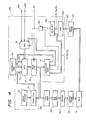
- Fig. 4 illustrates a specific operative example of the microcode sequencer 2D in connection with several other parts used in Fig. 1.
- a microcode memory 14 is shown to be separate from the pattern memory 2A.
- the microcode memory 14 and the pattern memory 2A are each read out by an address signal.from a program counter 15. From the microcode memory 14 are read out an instruction to be executed next, a branch address and so forth.
- the instruction read out of the microcode memory 14 is input into a microcode decoder 16, wherein it is interpreted.
- a microcode decoder 16 To the microcode decoder 16 are provided via input terminals 16A and 16B an interrupt signal (INTERRUPT) and a pause signal (PAUSE) as external control signals.
- an interrupt signal (INTERRUPT)
- a pause signal (PAUSE)
- IF signals external control signals indicating the status of the circuit under test 5 are applied via the input probe 2I to a terminal 16C.
- the address read out of the microcode memory 14 is provided to one input terminal 17A of a multiplexer 17.
- To another input terminal 17B of the multiplexer 17 is applied from an interrupt register 18 an address signal indicating an address to be jumped to at the time of an interruption, and still another input terminal 17C of the multiplexer 17 is supplied with an address signal from a stack file 19.
- the multiplexer 17 responds to the output of the microcode decoder 16 to select any one of the input terminals 17A, 17B and 17C to load the corresponding address into the program counter 15.
- the external control signals from the input probe 21 are plural, as mentioned above, and these external control signals are encoded by an encoder 16D.
- the encoded output B l B 2 B 3 and a status specifying code A l A 2 A 3 at the time of an IF instruction read out of the microcode memory 14 are compared by a coincidence detector 16E.
- a coincidence detector 16E When coincidence is detected, an inhibit gate 16F is disabled to inhibit the passage therethrough of a signal indicating the IF instruction to enable the microcode decoder 16, but when the signal indicating the IF instruction is applied to the microcode decoder 16, its operation is stopped.
- the instructions that are read out of the microcode memory 14 are INC, JUMP, CALL and RETURN instructions.
- the INC instruction is mainly read out.
- the count value of the program counter 15 is incremented by counting one PG clock pulse from the terminal 2b upon each occurrence of the INC instruction.to advance the addresses of the pattern memory 2A and the microcode memory 14 one by one, and pattern data is read out of the pattern memory 2A and applied to the signal generator 2G, generating a pattern signal.
- a branch address read out of the microcode memory 14, along with the instruction, is loaded via the multiplexer 17 into the program counter 15 and then an instruction of the branched address area is performed, creating a pattern signal defined by this address area.
- the microcode sequencer 2D stops execution of the program during the application of the PAUSE signal.
- an instruction to be read out of the microcode memory 14 is added with an IF statement, as required, and when the instruction added with the IF statement is read out, if the status code A 1 A 2 A 3 specified by the instruction and a signal representing the status of the circuit under test 5, applied to the external control input terminal 16C, that is, the output B 1 B 2 B 3 of the encoder 16D, coincide with each other, then the signal indicating the IF statement cannot pass through the inhibit gate 16F and the decoder 16 operates to perform the instruction added with the IF statement.
- the test starts with the execution of an instruction LOOP 1 to generate test pattern signals.
- the instruction A 1 A 2 A 3 IF CALL SUB 1 is read out.
- the status output from the circuit under test 5 will coincide with the status represented by the status code A 1 A 2 A 3 .
- the microcode decoder 16 performs the instruction IF CALL SUB 1, that is, the microcode decoder 16 jumps to an address being read out at that time and executes a subroutine SUB 1 to generate a series of test patterns and, at the end of the subroutine SUB 1, performs the RETURN instruction to return to the address pushed in the stack file 19 before it proceeded to the subroutine SUB 1, carrying out an instruction LOOP 2.
- the microcode decoder-16 after completing the execution of the instruction LOOP-1, the microcode decoder-16-responds to a jump instruction to return to the beginning of the instruction LOOP 1. This operation is repeatedly performed to test the circuit under test 5. If no coincidence is detected between the status codes A l A 2 A 3 and B l B 2 B 3 when the instruction A l A 2 A 3 IF CALL SUB 1 is read out, the instruction LOOP 2 will be further executed.
- the circuit under test 5 can be tested completely in all states. That is, according to the prior art, when the status of the circuit under test 5 satisfies a predetermined condition, the subroutine SUB 1 in the above example is performed, but it may sometimes be impossible, under the influence of an external signal, to predict when the circuit under test 5 reaches the condition (status), and in such an instance, the subroutine SUB 1 is carried out before the completion of the test desired to make.
- the display unit 9 has such an arrangement, for example, as depicted in Fig. 7.
- An address bus 4A in the bus line 4 is connected to a multiplexer 31, the output side of which is connected to an address input side of the video memory 9A.
- a data bus 4D is connected via a bus driver 32 to a data terminal of the video memory 9A.
- a control line 4C is connected to a control terminal of the multiplexer 31, a read/write control terminal of the video memory 9A and an input/output control terminal of the bus driver 32.
- a write into the video memory 9A from the control unit 3 (Fig.
- a readout address in synchronism with the abovesaid synchronizing signal is produced via the multiplexer 31 to the video memory 9A.
- the character data, which is read out of the video memory 9A is applied as an address to each of a character generator 38 and a graphic pattern generator 39.
- these generators 38 and 39 have stored therein, as dot patterns, the characters, the symbols and the partial graphic forms to be displayed..
- the corresponding dot patterns are read out of the generators 38 and 39.
- the outputs therefrom are converted by the parallel-serial converter 36 into a serial dot pattern, which is provided as a display signal to the display 9C via the video controller 37.
- the character, symbol and partial graphic form stored in the video memory 9A are displayed on the screen of the display 9C.
- the write from the control unit 3 to the video memory 9A is effected in the vertical or horizontal fly-back period (blanking period) of the display 9C.
- a partial graphic form corresponding to one character in the case of the pattern signal waveform being displayed on the screen of the display 9C is stored in the graphic pattern generator 39. That is, dot patterns representing such graphic pattern segments " ⁇ ", “ “ “ “ “ “ “”, “, “ “ and “n” as shown in Figs. 8A to 8F are stored in the graphic pattern generator 39 and character codes corresponding to them are respectively determined. When the graphic pattern generator 39 is read out using the character codes, the corresponding dot patterns are obtained.
- the signal generator 2G (Fig. 1) generates eight test patterns, they are displayed as A to H on the screen 40 of the display 9C and their polarities are also displayed with a sign + or -, and at the same time, the values of the delay time LD and the pulse width ⁇ W are displayed in a block indicated by the two-dot chain line in Fig. 9.
- the test pattern signal B is shown to be an NRZ waveform which is positive and has a delay time LD of 20 nsec but no pulse width ⁇ W
- the test pattern signal H is shown to be an RZ waveform which is negative and has a delay time TD of 60 nsec and a pulse width ⁇ W of 20 nsec.
- the numeric values of the test pattern signals A to H are displayed and, in this example, their waveforms Pa, Pb, Pc, ⁇ and Ph, which are determined by the numeric values and symbols, are also displayed side by side with the numeric values.
- a scale S for the waveforms is also displayed.
- waveform display data is created on the basis of the data for the test pattern signals A to H and stored in the video memory 9A.
- the waveform display data is prepared by the control unit 3.
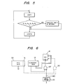
- Fig. 10 shows, in flowchart form, a program for preparing the waveform display data on the basis of the test pattern data and storing them in the video memory 9A.
- step S 1 a cursor 42 turns on and off in a clock period column CLK displayed on the screen of the display 9C shown in Fig. 9, urging to enter the period Ta of the PG clock.
- the delay time ⁇ D and the pulse width ⁇ W of the pattern signal waveforms Pa to Ph are set with resolution 1/10 the period Ta of the PG clock. That is, by setting the period Ta of the PG clock, the scale having 10 graduations corresponds to the set period Ta.
- Fig. 9 shows the case where the input means 11 is operated to set the period Ta to 100 nsec.
- step S 2 the cursor 42 turns on and off in the polarity column of the pattern signal A, urging to set the polarity of the pattern signal A.
- the operator can set the polarity of the pattern signal A by operating a (+) or (-) key.
- the pattern signal A is shown to be set to the positive polarity [+].
- step S 3 the cursor 42 turns on and off in the delay time column, indicating the state to input the delay time ⁇ D of the pattern signal A.
- step s 4 the cursor 42 turns on and off in the width column, indicating the state to input the width data ⁇ W + ⁇ D .
- Fig. 9 shows the case where the pulse width ⁇ W is set to zero. When the pulse width ⁇ W is set to zero, the pattern generator 2 generates the NRZ waveform.
- step S 5 a check is made to determine if the set pulse width ⁇ W is zero or not, and if so, the program branches to a routine L A .
- step S 7 the character code of the graphic pattern segment "X" in Fig. 8A indicating a signal switching point of the NRZ waveform, is stored in the video memory 9A at an address corresponding to the delay point.
- the routine L ends at step S 8 .
- the video memory 9A is held in the readout state except a write is effected therein, and its contents are displayed on the display 9C.
- the signal A is displayed as the waveform Pa side by side with the symbols and numeric values indicating the signal A, as shown in Fig. 9. Taking a glance at the waveform Pa, the operator will readily understand that it is an NRZ waveform and that the delay time TD is zero.
- step S 9 it is decided whether a key input for completing the.setting is present or not. If not, then the process goes back to step S 2 to urge the setting of the signal B.
- the pattern waveform Pb of the signal B is displayed side by side with its numeric values.
- the signals A to D are shown to be set to zero in pulse width. Accordingly, NRZ waveforms Pa, Pb, Pc and Pd are displayed in the waveform columns of the signals A to D.
- the delay times ⁇ D of the signals B, C and D are shown to be set to 20, 40 and 60 nsec, respectively.
- the signal E is shown to have a pulse width ⁇ W of 20 nsec.
- the pulse width ⁇ W is set to a numeric value except zero, an RZ waveform is produced. That is, when the pulse width ⁇ W is not zero, the program branches to step S10 from step S 5 .
- step S 10 it is decided whether the polarity being set is positive or not. If the polarity is positive (+), the program branches to a routine L B .
- the routine L B starts at step S 11 , in which the character code representing an L logic level line of the RZ waveform, i.e. the graphic pattern segment " " in Fig. 8D is stored in the corresponding address area of the video memory 9A from the origin to the delay point.
- the delay time LD is shown to be set to 30 nsec. In consequence, the L logic line is displayed by three graduations of the scale S from the origin in the waveform column of the signal E.
- step S 12 the character code representing the leading edge waveform of a positive pulse, i.e. the graphic pattern segment in Fig. 8E is written in the address area of the video memory 9A which corresponds to the delay point.
- step S 13 the character code representing an H logic line, i.e. the graphic pattern segment in Fig. 8C is written in the video memory 9A at the corresponding addresses equal to the pulse width ⁇ W .
- step S 14 the character code representing the trailing edge waveform, i.e. the graphic pattern segment in Fig. 8B, is written in the video memory 9A at addresses corresponding to ( ⁇ D + T w ).
- step S 15 the character code representing the L logic line, i.e. the graphic pattern segment in Fig. 8D, is written in the video memory 9A to the end point.
- the routine L B ends at step S 15 , and it is decided in step S 9 whether the key input for the completion of the setting procedure is present or not. If not, the process returns to step S 2 .
- step S 10 When the polarity is set to (-) in step (2), the program branches to a routine L C from step S 10 .
- routine L C a negative pattern signal waveform is written in a waveform storage area of the video memory 9A corresponding to the signal set to be negative. That is, in step S16 the character code of the graphic pattern segment in Fig. 8C is written in the video memory 9A from the origin to the delay point.
- step S 17 the character code of the graphic pattern segment in Fig. 8B is written in the video memory 9A corresponding to the delay point.
- step S18 the character code of the graphic pattern segment in Fig. 8D is written in the video memory 9A by the pulse width ⁇ W being set.
- step S 19 the character code of the graphic pattern segment in Fig. 8E is written in the video memory 9A corresponding to the position of ( TD + TW ).
- step S 20 the character code of the graphic pattern segment in Fig. 8C is written in the video memory 9A to the end point.
- the signals G and H are shown to be set negative (-), and negative pattern signal waveforms Pg and Ph are displayed correspondingly.
- step S 9 When the setting end command is detected in step S 9 , the program branches to step S 21 , in which the video memory 9A is switched to a continuous read mode, completing the setting program.
- the screen 40 of the display 9C includes a numeric value display area on the upper left and a waveform display area on the upper right and, further, a display area on the lower side indicating which one of thus set pattern signals is being output from each channel of the output probe 6 (Fig. 1).
- this example shows the state in which the pattern signal A is being output in all channels 0 to 15 (where A indicates the channel 10 and F the channel 15) of the probe group A; the state in which the pattern signal B is being output in all channels 0 to 15 of the probe group B; the state in which the pattern signal C is being output in channels 0 to 9 of the probe group C, the pattern signal B in channels 10 and 11 and the pattern signal A in channels 12 to 15; and the state in which the pattern signal D is being output in channels 0 to 15 of the probe group D.
- the present invention it is possible to output a desired pattern signal in a desired channel of each probe, as mentioned above.
- the present invention offers the advantage that the pattern data can be set easily and without fail.
- period Ta is divided into 10 graduations of the scale S
- the number of division can be selected as desired.
- the character generator 38 and the graphic pattern generator 39 can also be constructed as one unit.
Landscapes
- Engineering & Computer Science (AREA)
- General Engineering & Computer Science (AREA)
- Physics & Mathematics (AREA)
- General Physics & Mathematics (AREA)
- Theoretical Computer Science (AREA)
- Computer Hardware Design (AREA)
- Quality & Reliability (AREA)
- Tests Of Electronic Circuits (AREA)
Applications Claiming Priority (4)
| Application Number | Priority Date | Filing Date | Title |
|---|---|---|---|
| JP59108920A JPH0614102B2 (ja) | 1984-05-28 | 1984-05-28 | 回路試験装置 |
| JP108919/84 | 1984-05-28 | ||
| JP59108919A JPS60252278A (ja) | 1984-05-28 | 1984-05-28 | ロジツクアナライザ |
| JP108920/84 | 1984-05-28 |
Publications (3)
| Publication Number | Publication Date |
|---|---|
| EP0163267A2 true EP0163267A2 (de) | 1985-12-04 |
| EP0163267A3 EP0163267A3 (en) | 1988-10-05 |
| EP0163267B1 EP0163267B1 (de) | 1993-10-13 |
Family
ID=26448742
Family Applications (1)
| Application Number | Title | Priority Date | Filing Date |
|---|---|---|---|
| EP85106364A Expired - Lifetime EP0163267B1 (de) | 1984-05-28 | 1985-05-23 | Logikanalysator |
Country Status (3)
| Country | Link |
|---|---|
| US (1) | US4701918A (de) |
| EP (1) | EP0163267B1 (de) |
| DE (1) | DE3587620T2 (de) |
Families Citing this family (14)
| Publication number | Priority date | Publication date | Assignee | Title |
|---|---|---|---|---|
| JPS6193962A (ja) * | 1984-10-15 | 1986-05-12 | Anritsu Corp | パタ−ントリガ付オシロスコ−プ |
| JPS62140299A (ja) * | 1985-12-13 | 1987-06-23 | Advantest Corp | パタ−ン発生装置 |
| DE3611872C1 (de) * | 1986-04-09 | 1987-04-30 | Rohle & Schwarz Gmbh & Co Kg | Logikanalysator |
| US4777616A (en) * | 1986-05-12 | 1988-10-11 | Outlook Technology, Inc. | Increased resolution logic analyzer using asynchronous sampling |
| US4860291A (en) * | 1987-12-28 | 1989-08-22 | Tektronix, Inc. | Test vector definition system employing template concept |
| US5282213A (en) * | 1991-01-02 | 1994-01-25 | Compaq Computer Corporation | Computer-based logic analyzer timing and analysis system |
| JP2882426B2 (ja) * | 1991-03-29 | 1999-04-12 | 株式会社アドバンテスト | アドレス発生装置 |
| US5327076A (en) * | 1992-09-17 | 1994-07-05 | Micro Control Company | Glitchless test signal generator |
| US6594789B2 (en) * | 1997-09-16 | 2003-07-15 | Texas Instruments Incorporated | Input data capture boundary cell connected to target circuit output |
| US6381506B1 (en) * | 1996-11-27 | 2002-04-30 | Victor Grappone | Fail-safe microprocessor-based control and monitoring of electrical devices |
| DE19711097C2 (de) * | 1997-03-17 | 2000-04-06 | Siemens Ag | Integrierte Schaltung mit einem Speicher und einer Prüfschaltung |
| US6202186B1 (en) * | 1999-01-29 | 2001-03-13 | Credence Systems Corporation | Integrated circuit tester having pattern generator controlled data bus |
| US6396517B1 (en) | 1999-03-01 | 2002-05-28 | Agilent Technologies, Inc. | Integrated trigger function display system and methodology for trigger definition development in a signal measurement system having a graphical user interface |
| US6535999B1 (en) * | 1999-07-13 | 2003-03-18 | Micron Technology, Inc. | Test and observe mode for embedded memory |
Family Cites Families (12)
| Publication number | Priority date | Publication date | Assignee | Title |
|---|---|---|---|---|
| US3750135A (en) * | 1971-10-15 | 1973-07-31 | Lektromedia Ltd | Low resolution graphics for crt displays |
| US3909792A (en) * | 1973-02-26 | 1975-09-30 | American Optical Corp | Electrocardiographic review system |
| US4216374A (en) * | 1978-08-11 | 1980-08-05 | John Fluke Mfg. Co., Inc. | Hybrid signature test method and apparatus |
| US4313200A (en) * | 1978-08-28 | 1982-01-26 | Takeda Riken Kogyo Kabushikikaisha | Logic test system permitting test pattern changes without dummy cycles |
| US4467324A (en) * | 1980-06-27 | 1984-08-21 | Del Mar Avionics | Apparatus and method for printing annotated electrocardial data |
| JPS6020755B2 (ja) * | 1980-12-26 | 1985-05-23 | 松下電器産業株式会社 | 画面表示装置 |
| US4434488A (en) * | 1981-06-08 | 1984-02-28 | Tektronix, Inc. | Logic analyzer for a multiplexed digital bus |
| US4425643A (en) * | 1981-06-08 | 1984-01-10 | Tektronix, Inc. | Multi-speed logic analyzer |
| US4450560A (en) * | 1981-10-09 | 1984-05-22 | Teradyne, Inc. | Tester for LSI devices and memory devices |
| US4503536A (en) * | 1982-09-13 | 1985-03-05 | General Dynamics | Digital circuit unit testing system utilizing signature analysis |
| JPS5997065A (ja) * | 1982-11-25 | 1984-06-04 | Advantest Corp | 論理回路試験装置の試験パタ−ン発生装置 |
| US4601033A (en) * | 1984-01-16 | 1986-07-15 | Siemens Corporate Research & Suppport, Inc. | Circuit testing apparatus employing signature analysis |
-
1985
- 1985-05-23 EP EP85106364A patent/EP0163267B1/de not_active Expired - Lifetime
- 1985-05-23 DE DE85106364T patent/DE3587620T2/de not_active Expired - Fee Related
- 1985-05-24 US US06/737,467 patent/US4701918A/en not_active Expired - Fee Related
Also Published As
| Publication number | Publication date |
|---|---|
| US4701918A (en) | 1987-10-20 |
| DE3587620T2 (de) | 1994-03-24 |
| EP0163267B1 (de) | 1993-10-13 |
| DE3587620D1 (de) | 1993-11-18 |
| EP0163267A3 (en) | 1988-10-05 |
Similar Documents
| Publication | Publication Date | Title |
|---|---|---|
| US4701918A (en) | Logic analyzer | |
| US4970664A (en) | Critical path analyzer with path context window | |
| EP0163273B1 (de) | Logikanalysator | |
| EP0159588B1 (de) | Logikanalysator | |
| US11677418B2 (en) | Error rate measuring apparatus and uncorrectable codeword search method | |
| JP2012208830A (ja) | プログラムテスト装置、プログラムテスト方法、およびプログラム | |
| NL8303721A (nl) | Werkwijze en inrichting voor syntax foutcorrectie. | |
| EP0093229A1 (de) | Vorrichtung und Verfahren zum Testen | |
| US4516119A (en) | Logic signal display apparatus | |
| EP1357389A2 (de) | Elektronisches Prüfprogramm mit Ausführungsauswahl | |
| US5130646A (en) | Circuit for connecting sequentially a plurality of devices to be tested to a tester apparatus | |
| US5434805A (en) | Test timing program automatic generator | |
| JP3214356B2 (ja) | テスト支援装置 | |
| JPH0148983B2 (de) | ||
| JP3672025B2 (ja) | テスト支援システム | |
| JPS58216961A (ja) | ロジツク・アナライザ | |
| KR960002275B1 (ko) | 집적회로 검사장치 | |
| KR100329942B1 (ko) | 캐릭터표시제어회로 | |
| JPH05150009A (ja) | テスト設計装置 | |
| JP2000149593A (ja) | Ic試験装置 | |
| GB1591448A (en) | Systems for performing sequences of electrical tests | |
| JPH0136907B2 (de) | ||
| SU1111166A1 (ru) | Логический анализатор | |
| JPH02126287A (ja) | 表示装置 | |
| KR20020033079A (ko) | 번인 시험 프로그램의 시뮬레이션 장치 및 방법과 기억매체 |
Legal Events
| Date | Code | Title | Description |
|---|---|---|---|
| PUAI | Public reference made under article 153(3) epc to a published international application that has entered the european phase |
Free format text: ORIGINAL CODE: 0009012 |
|
| 17P | Request for examination filed |
Effective date: 19850523 |
|
| AK | Designated contracting states |
Designated state(s): DE GB NL |
|
| PUAL | Search report despatched |
Free format text: ORIGINAL CODE: 0009013 |
|
| AK | Designated contracting states |
Kind code of ref document: A3 Designated state(s): DE GB NL |
|
| 16A | New documents despatched to applicant after publication of the search report | ||
| 17Q | First examination report despatched |
Effective date: 19910218 |
|
| GRAA | (expected) grant |
Free format text: ORIGINAL CODE: 0009210 |
|
| AK | Designated contracting states |
Kind code of ref document: B1 Designated state(s): DE GB NL |
|
| REF | Corresponds to: |
Ref document number: 3587620 Country of ref document: DE Date of ref document: 19931118 |
|
| PG25 | Lapsed in a contracting state [announced via postgrant information from national office to epo] |
Ref country code: GB Effective date: 19940523 |
|
| PLBE | No opposition filed within time limit |
Free format text: ORIGINAL CODE: 0009261 |
|
| STAA | Information on the status of an ep patent application or granted ep patent |
Free format text: STATUS: NO OPPOSITION FILED WITHIN TIME LIMIT |
|
| 26N | No opposition filed | ||
| PG25 | Lapsed in a contracting state [announced via postgrant information from national office to epo] |
Ref country code: NL Effective date: 19941201 |
|
| NLV4 | Nl: lapsed or anulled due to non-payment of the annual fee | ||
| GBPC | Gb: european patent ceased through non-payment of renewal fee |
Effective date: 19940523 |
|
| PG25 | Lapsed in a contracting state [announced via postgrant information from national office to epo] |
Ref country code: DE Effective date: 19950201 |