EP0163580A2 - Halbleiterintegrierte Schaltung mit einer Ersatzredundanzschaltung - Google Patents
Halbleiterintegrierte Schaltung mit einer Ersatzredundanzschaltung Download PDFInfo
- Publication number
- EP0163580A2 EP0163580A2 EP85401065A EP85401065A EP0163580A2 EP 0163580 A2 EP0163580 A2 EP 0163580A2 EP 85401065 A EP85401065 A EP 85401065A EP 85401065 A EP85401065 A EP 85401065A EP 0163580 A2 EP0163580 A2 EP 0163580A2
- Authority
- EP
- European Patent Office
- Prior art keywords
- circuit
- transistor
- transistors
- circuit according
- address
- Prior art date
- Legal status (The legal status is an assumption and is not a legal conclusion. Google has not performed a legal analysis and makes no representation as to the accuracy of the status listed.)
- Granted
Links
Images


Classifications
-
- G—PHYSICS
- G11—INFORMATION STORAGE
- G11C—STATIC STORES
- G11C29/00—Checking stores for correct operation ; Subsequent repair; Testing stores during standby or offline operation
-
- G—PHYSICS
- G11—INFORMATION STORAGE
- G11C—STATIC STORES
- G11C29/00—Checking stores for correct operation ; Subsequent repair; Testing stores during standby or offline operation
- G11C29/70—Masking faults in memories by using spares or by reconfiguring
- G11C29/78—Masking faults in memories by using spares or by reconfiguring using programmable devices
- G11C29/835—Masking faults in memories by using spares or by reconfiguring using programmable devices with roll call arrangements for redundant substitutions
Definitions
- the present invention relates to an integrated circuit having memory cells.
- the integrated circuit according to the present invention is used for a memory device having a redundant circuit portion for replacing failed circuits.
- an integrated circuit device for a semiconductor memory is provided with "redundant-bit" type memory cells in addition to the usually used memory cells. These are used to replace failed memory cells or even to replace an entire bit line containing failed memory cells, in the latter case by a redundant bit line containing redundant memory cells. This increases the yield of the products in-the manufacture of integrated circuits.
- ROM's read-only memories
- the circuit is switched to access a redundant memory cell instead of the failed memory cell. Accordingly, quick and correct detection of the written state of the ROM's is important.
- a semiconductor integrated circuit including a memory unit for storing address information of a failed circuit portion for replacing the failed circuit portion by a redundant circuit portion; a comparison unit for detecting coincidence between data read from the memory unit and a received input address; and a delivery unit for delivering data obtained from the comparison by the comparison unit through an external connection terminal.
- Fig. 1 is block diagram of a prior art integrated circuit
- the device of Fig. 1 includes coincidence detection circuits 2, 2, ..., corresponding to the number of bits of the input address signals A 0 , A 1 , ... A n , and a depletion type transistor 32 as a load transistor.
- Non-inverted and inverted address signals A 0 , A 0 , A 1 , A 1 , ... An and An are supplied to the coincidence detection circuits 2, 2 ...
- Each of the coincidence detection circuits carries out a comparison between the input address signal and the stored address signal in a ROM in the coincidence detection circuit.
- the potential of the control line 31 (N l ) becomes HIGH, while when one or more of the coincidence detection circuits does not indicate coincidence, the potential of the control line 31 (N 1 ) becomes LOW.
- the ROM's in the coincidence detection circuits store the address of failed memory cell.
- the potential of the control line 31 (N 1 ) becomes HIGH.
- a redundant memory cell is accessed instead of the failed memory cell.
- a fuse 211 and a transistor 213 constitute a fuse blow-out type ROM.
- One bit of the address information of a failed memory cell is stored in this ROM.
- Transistors 231 and 232 constitute an inverter circuit.
- Transistors 241 to 244 constitute a comparison circuit in the form of an exclusvie OR gate circuit. The series-connected transistors 241 and 242 and the series-connected transistors 243 and 244 are connected between the control line 31 (N 1 ) and the voltage source line V ss .
- the gate of the transistor 241 is connected to the output node N 2 of the inverter circuit (231, 232).
- the gate of the transistor 243 is connected to the output node N 3 of the fuse blow-out type ROM (211, 213).
- the non-inverted address signal A is supplied to the gate of the transistor 242, while the inverted address signal A is supplied to the gate of the transistor 244.
- the fuse blow-out type ROM (211, 212) stores the address data "0" by the blown state of the fuse 211 and stores the address date "1" by the non-blown state of the fuse 211.
- the potential of the control line 31 (N 1 ) becomes HIGH.
- Figure 3 shows another example of the structure of the coincidence detection circuits 2, 2, ... shown in Fig. 1.
- the ROM portion of the coincidence detection circuit of Fig. 3 includes a series-connected fuse 211 and a depletion type transistor 213, a series-connected fuse 212 and a depletion type transistor 214, and a NAND gate circuit consisting of a series-connected depletion type transistor 221, enhancement type transistor 222, and enhancement type transistor 223.
- ... A n are changed successively from “0, 0, ... 0" to "1, 1, ... 1", and the values of the address signals which make the potential of the control line 31 (N 1 ) HIGH is inspected.
- the values of the address signals A 0 , A 1 ... A n which make the potential of the control line 13 (N 1 ) HIGH indicate the address of the failed portion.
- FIG. 4 A semiconductor integrated circuit according to an embodiment of the present invention is illustrated in Fig. 4.
- the circuit of Fig. 4 includes coincidence detection circuits 2, 2, ..., a load transistor 32, an output circuit consisting of transistors 61 and 62, and an external connection terminal 7.
- the transistor 32 is connected between a voltage source V cc and the control line 31 (N 1 ) and is operated as a pull-up circuit or a load circuit.
- the transistors 61 and 62 are connected in series between the voltage source V ss and an external connection terminal 7.
- the gate of the transistor 61 is connected with the control line 31 (N 1 ), while the gate of the transistor 62 is connected with the junction of the transistors 61 and 62.
- the external connection terminal 7 may be used also for a terminal for another signal.
- Non-inverted and inverted signals A 0 , A 0 , A 1 , A 1 , ... A n , A n are supplied to the coincidence detection circuit 2, 2, ... in the circuit of Fig. 4.
- the input address signals are compared with the address signals stored in the ROM's in the coincidence detection circuits. When the compared signals coincide, the impedance between the output terminal of the coincidence detection circuit connected with the control line 31 (N 1 ) and the voltage source V ss becomes HIGH. When the compared signals do not coincide, the above-mentioned impedance becomes LOW.
- a redundant memory call is accessed instead of a failed memory cell only when the potential of the control line 31 (N 1 ) is HIGH. Such an arrangement endless automatic switching from the failed memory cell to the redundant memory cell.
- Various tests of the integrated circuit can be carried out conveniently by using the information concerning failed bits stored in the ROM's in the ' coincidence detection circuits.
- the detection of the information stored in the ROM's is carried out by inputting a sequence of varying addressee A 0 , A 1 ... An and detecting sequentially the potentials of the external connection terminal 7 accordingly.
- the indication of a resistor 8 and a voltage source V , for example -3V, in broken lines is for explaining how current flows through the external connection terminal 7 after application of a voltage V x through the resistor 8 to the external connection terminal 7.
- the coincidence detection circuit shown in Fig. 2 is used for each of the coincidence detection circuits 2, 2, ... in the circuit shown in Fig. 4.
- FIG. 5 A semiconductor integrated circuit according to another embodiment of the present invention is illustrated in Fig. 5.
- Each of the coincidence detection circuits 2, 2, ... in the circuit shown in Fig. 5 has two output terminals, one connected with a control line 31 (N 1 ), the other connected with a detection line 4 1 (N 21 ).
- Each of the coincidence detection circuits 2, 2, ... includes a memory portion 21, a comparison portion 24, and a status detection portion 25.
- the structure of the coincidence detection circuit 2 is illustrated in Fig. 6.
- the status detection portion 25 includes transistors 2501 and 2502, which are connected in series between a detection line 41 (N 2l ) and a voltage source V .
- the gate of the transistor 2501 is connected to a node N 3 in the ROM 21.
- the gate of the transistor 2502 receives the input signal A.
- the impedance between the control line 31 (N 1 ) and the voltage source V ss is HIGH when the potentials of the nodes N 3 and N 2 conform to the input signals A and A, while the impedance is LOW when the potentials of the nodes N 3 and N 2 do not conform to the input signal A and A .
- the potential of the input signal A is made HIGH in order to detect the storage state of the ROM 21, that is, the state of the fuse 211.
- the transistor 2502 becomes ON, and the information of the state of the fuse 211 is output to the detection line 41 (N 21).
- the potential of the node N 3 is LOW, and the transistor 2501 becomes OFF. Accordingly, the impedance between the control line 31 (N 1 ) and the voltage source V ss is HIGH. Hence, the potential of the detection line 41 (N 21 ) becomes HIGH due to the operation of the depletion type transistor 42 (Fig. 5) connected between the detection line 41 (N21) and the voltage source V cc , so that the blown state of the fuse 211 is detected.
- FIG. 7 Another example of the structure of the coincidence detection circuit is shown in Fig. 7.
- the circuit of Fig. 7 is similar to the circuit of Fig. 3, except that the status detection circuit 25 consisting of transistors 2503 to 2507 is added.
- a non-inverted selection signal A n+1 and an inverted selection signal A n+1 are applied to the gates of the transistors 2505 and 2507.
- a non-inverted address signal A is applied to the gate of the transistor 2503.
- the address signal A and the non-inverted signals A n+1 are made HIGH. Hence, the transistors 2503 and 2505 becomes ON.
- the address signal A HIGH and the selection signal A n+1 LOW, that is, the selection signal An+, HIGH the information of the state of the fuse 212 is output to the detection line 41 (N 21 ).
- the state of each of the fuses 211 and 212 can be detected separately.
- the circuit of Fig. 7 is particularly useful for the case where the memory cell matrix is divided by rows or by columns to be divided into a plurality of blocks in which the switching to the redundant circuit is carried out simultaneously in parallel with regard to the plurality of blocks.
- the circuit of Fig. 8 includes a status detection circuit 25, consisting of the transistors 2508 to 2511, and detection lines 41 (N21) and 51 (N 31 ).
- Series-connected transistors 2508 and 2509 are connected between the detection line 41 (N 21 ) and the voltage source V ss
- series-connected transistors 2510 and 2511 are connected between the detection line 51 (N 31 ) and the voltage source V ss .
- the gates of the transistors 2508 and 2510 are connected to the nodes N 4 and N 5 .
- the gates of the transistors 2509 and 2511 receive the address signal A.
- the transistors 2509 and 2511 are caused to be ON by making the address signal A high. Under this condition, when the fuse 211 is blown, the potential of the node N 4 is LOW, the transistor 2508 is OFF, and, accordingly, the potential of the detection line 41 (N 21 ) becomes HIGH. When the fuse 211 is not blown, the potential of the node N 4 is HIGH, the transistor 2508 is ON, and, accordingly, the potential of the detection line 41 (N 21 ) becomes LOW.
- the transistor 2510 is OFF, and, accordingly, the potential of the detection line 51 (N 31 ) becomes HIGH.
- the transistor 2510 is ON, and, accordingly, the potential of the detection line 51 (N31) becomes LOW.
- the address signal is increased successively by one bit for detecting the state of the ROM corresponding to each of the bits of the address signal.
- an inverted address signal A instead of a non-inverted address signal A, is supplied to the gate of the transistor 2502, it is possible to detect the state of the fuse 211 by making the address signal A LOW.
- the address signal applied to the transistor 2502 By making the address signal applied to the transistor 2502 to be, bit by bit, a non-inverted address signal or an inverted address signal, it is possible to select any pattern of address signals for detecting the written state of the ROM.
- Table (A) indicates the address signal supplied to the gate of the transistor 2502.
- Table (B) indicates the address pattern for detecting the state of the ROM.
- the circuit of Fig. 9 includes a status detection circuit 25 consisting of transistors 2512, 2521, 2522, ... 252k.
- the gate of the transistor 2512 receives the potential of the node N 3 which represent the state of the fuse 211.
- the gates of the transistors 2521, 2522, ... 252k receive either one of the non-inverted signals A (A 0 , A 1 , ... An) or one of the inverted signals A ( A 0 , A 1 , ... A n ) of the corresponding bit of the input address.
- 2 k+1 status detection circuits can be realized so that the detection of the states of 2 k+1 fuses can be carried out.
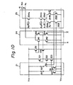
- FIG. 10 A further example of the structure of the coincidence detection circuit is shown in Fig. 10.
- the circuit of Fig. 10 includes a status detection circuit 25 consisting of transistors 2531, 2532, 2541a, 2541b, 2542, 2543, ... 254k.
- the operation of the circuit of Fig. 10 will be apparent from the operations of the circuit of Fig. 7 and the circuit of Fig. 9.
Landscapes
- For Increasing The Reliability Of Semiconductor Memories (AREA)
- Techniques For Improving Reliability Of Storages (AREA)
- Tests Of Electronic Circuits (AREA)
Applications Claiming Priority (4)
| Application Number | Priority Date | Filing Date | Title |
|---|---|---|---|
| JP59109463A JPS60254499A (ja) | 1984-05-31 | 1984-05-31 | 記憶装置の作動状態の検査を行うことができる、冗長機能を有する半導体集積回路装置 |
| JP109463/84 | 1984-05-31 | ||
| JP153942/84 | 1984-07-26 | ||
| JP15394284A JPS6134799A (ja) | 1984-07-26 | 1984-07-26 | 半導体集積回路装置 |
Publications (3)
| Publication Number | Publication Date |
|---|---|
| EP0163580A2 true EP0163580A2 (de) | 1985-12-04 |
| EP0163580A3 EP0163580A3 (en) | 1988-08-31 |
| EP0163580B1 EP0163580B1 (de) | 1996-09-04 |
Family
ID=26449211
Family Applications (1)
| Application Number | Title | Priority Date | Filing Date |
|---|---|---|---|
| EP85401065A Expired - Lifetime EP0163580B1 (de) | 1984-05-31 | 1985-05-30 | Halbleiterintegrierte Schaltung mit einer Ersatzredundanzschaltung |
Country Status (4)
| Country | Link |
|---|---|
| US (1) | US4752914A (de) |
| EP (1) | EP0163580B1 (de) |
| KR (1) | KR900008191B1 (de) |
| DE (1) | DE3588121T2 (de) |
Cited By (2)
| Publication number | Priority date | Publication date | Assignee | Title |
|---|---|---|---|---|
| EP0509633A3 (en) * | 1991-03-07 | 1993-02-03 | Sharp Kabushiki Kaisha | Semiconductor memory |
| EP0520449A3 (en) * | 1991-06-27 | 1995-05-10 | Nippon Electric Co | Semiconductor memory device |
Families Citing this family (16)
| Publication number | Priority date | Publication date | Assignee | Title |
|---|---|---|---|---|
| JPS6267800A (ja) * | 1985-09-20 | 1987-03-27 | Hitachi Ltd | 半導体集積回路装置 |
| JPS62250593A (ja) * | 1986-04-23 | 1987-10-31 | Hitachi Ltd | ダイナミツク型ram |
| US4942575A (en) * | 1988-06-17 | 1990-07-17 | Modular Computer Systems, Inc. | Error connection device for parity protected memory systems |
| US5617365A (en) * | 1988-10-07 | 1997-04-01 | Hitachi, Ltd. | Semiconductor device having redundancy circuit |
| US5157634A (en) * | 1990-10-23 | 1992-10-20 | International Business Machines Corporation | Dram having extended refresh time |
| US5276834A (en) * | 1990-12-04 | 1994-01-04 | Micron Technology, Inc. | Spare memory arrangement |
| EP0519669A3 (en) * | 1991-06-21 | 1994-07-06 | Ibm | Encoding and rebuilding data for a dasd array |
| WO1993021578A1 (de) * | 1992-04-16 | 1993-10-28 | Siemens Aktiengesellschaft | Integrierter halbleiterspeicher mit redundanzeinrichtung |
| JPH10334694A (ja) * | 1997-05-30 | 1998-12-18 | Toshiba Corp | 半導体記憶装置 |
| JP2001060399A (ja) * | 1999-08-20 | 2001-03-06 | Fujitsu Ltd | 半導体記憶装置 |
| DE10201431C1 (de) * | 2002-01-16 | 2003-08-21 | Infineon Technologies Ag | Integrierte Schaltung und Verfahren zum Betrieb einer Testanordnung mit einer integrierten Schaltung |
| JP4062247B2 (ja) * | 2003-12-11 | 2008-03-19 | ソニー株式会社 | 半導体記憶装置 |
| KR100909358B1 (ko) * | 2007-04-16 | 2009-07-24 | 삼성전자주식회사 | 신뢰성 높은 초기화 데이터를 제공하는 플래시 메모리 장치및 그것의 초기화 방법 |
| US8839053B2 (en) * | 2010-05-27 | 2014-09-16 | Microsoft Corporation | Error correcting pointers for non-volatile storage |
| US9032244B2 (en) | 2012-11-16 | 2015-05-12 | Microsoft Technology Licensing, Llc | Memory segment remapping to address fragmentation |
| CN120853633A (zh) * | 2024-04-26 | 2025-10-28 | 长江存储科技有限责任公司 | 存储器装置及其操作方法、存储器系统 |
Family Cites Families (8)
| Publication number | Priority date | Publication date | Assignee | Title |
|---|---|---|---|---|
| JPS5818719B2 (ja) * | 1975-08-18 | 1983-04-14 | 株式会社リコー | Rom バツクアツプソウチ |
| US4346459A (en) * | 1980-06-30 | 1982-08-24 | Inmos Corporation | Redundancy scheme for an MOS memory |
| WO1982002793A1 (en) * | 1981-02-02 | 1982-08-19 | Otoole James E | Semiconductor memory redundant element identification circuit |
| US4480199A (en) * | 1982-03-19 | 1984-10-30 | Fairchild Camera & Instrument Corp. | Identification of repaired integrated circuits |
| US4538245A (en) * | 1982-04-12 | 1985-08-27 | Seeq Technology, Inc. | Enabling circuit for redundant word lines in a semiconductor memory array |
| US4546454A (en) * | 1982-11-05 | 1985-10-08 | Seeq Technology, Inc. | Non-volatile memory cell fuse element |
| JPS6018899A (ja) * | 1983-07-13 | 1985-01-30 | Toshiba Corp | 半導体メモリ |
| US4571707A (en) * | 1984-02-23 | 1986-02-18 | Nec Corporation | Memory circuit with improved redundant structure |
-
1985
- 1985-05-30 DE DE3588121T patent/DE3588121T2/de not_active Expired - Fee Related
- 1985-05-30 EP EP85401065A patent/EP0163580B1/de not_active Expired - Lifetime
- 1985-05-30 US US06/739,159 patent/US4752914A/en not_active Expired - Lifetime
- 1985-05-31 KR KR1019850003795A patent/KR900008191B1/ko not_active Expired
Cited By (2)
| Publication number | Priority date | Publication date | Assignee | Title |
|---|---|---|---|---|
| EP0509633A3 (en) * | 1991-03-07 | 1993-02-03 | Sharp Kabushiki Kaisha | Semiconductor memory |
| EP0520449A3 (en) * | 1991-06-27 | 1995-05-10 | Nippon Electric Co | Semiconductor memory device |
Also Published As
| Publication number | Publication date |
|---|---|
| EP0163580A3 (en) | 1988-08-31 |
| US4752914A (en) | 1988-06-21 |
| DE3588121D1 (de) | 1996-10-10 |
| DE3588121T2 (de) | 1997-01-16 |
| EP0163580B1 (de) | 1996-09-04 |
| KR900008191B1 (ko) | 1990-11-05 |
| KR850008566A (ko) | 1985-12-18 |
Similar Documents
| Publication | Publication Date | Title |
|---|---|---|
| EP0163580A2 (de) | Halbleiterintegrierte Schaltung mit einer Ersatzredundanzschaltung | |
| EP0034070B1 (de) | Fehler tolerierendes Speichersystem | |
| US4685086A (en) | Memory cell leakage detection circuit | |
| EP0031386A1 (de) | Halbleiter-speichervorrichtung | |
| US4428068A (en) | IC with built-in electrical quality control flag | |
| US4586170A (en) | Semiconductor memory redundant element identification circuit | |
| US6160745A (en) | Semiconductor storage device | |
| US4654830A (en) | Method and structure for disabling and replacing defective memory in a PROM | |
| EP0121394A2 (de) | Statisches Halbleiterspeichergerät mit eingebauten Redundanzspeicherzellen | |
| US4860256A (en) | Integrated circuit provided with switching elements for changeover to redundancy elements in a memory | |
| EP0086310B1 (de) | Integrierte Halbleiterschaltung mit Prüfschaltung | |
| US4783781A (en) | Semiconductor memory device having redundancy configuration with read circuit for defective memory address | |
| EP0188013A1 (de) | Kurzschlussdetektor für durchbrennbare Schaltbrücken mit einer Anordnung von Referenzschaltbrücken | |
| US4731759A (en) | Integrated circuit with built-in indicator of internal repair | |
| US4729117A (en) | Semiconductor memory device | |
| US4731760A (en) | On-chip test circuitry for an ECL PROM | |
| US5255217A (en) | Integrated circuit memory device with a redundant memory block | |
| JPH07312100A (ja) | 半導体メモリ集積回路 | |
| US11335427B1 (en) | Memory test circuit | |
| US4489402A (en) | Semiconductor memory device | |
| JPS5896744A (ja) | 半導体メモリ | |
| JPH0349160B2 (de) | ||
| JPS59129999A (ja) | 半導体メモリ装置 | |
| WO1982002792A1 (en) | Semiconductor memory cell margin test circuit | |
| JPH0541099A (ja) | 半導体記憶装置 |
Legal Events
| Date | Code | Title | Description |
|---|---|---|---|
| PUAI | Public reference made under article 153(3) epc to a published international application that has entered the european phase |
Free format text: ORIGINAL CODE: 0009012 |
|
| AK | Designated contracting states |
Designated state(s): DE FR GB |
|
| PUAL | Search report despatched |
Free format text: ORIGINAL CODE: 0009013 |
|
| AK | Designated contracting states |
Kind code of ref document: A3 Designated state(s): DE FR GB |
|
| 17P | Request for examination filed |
Effective date: 19881228 |
|
| 17Q | First examination report despatched |
Effective date: 19901026 |
|
| GRAH | Despatch of communication of intention to grant a patent |
Free format text: ORIGINAL CODE: EPIDOS IGRA |
|
| GRAH | Despatch of communication of intention to grant a patent |
Free format text: ORIGINAL CODE: EPIDOS IGRA |
|
| GRAA | (expected) grant |
Free format text: ORIGINAL CODE: 0009210 |
|
| AK | Designated contracting states |
Kind code of ref document: B1 Designated state(s): DE FR GB |
|
| REF | Corresponds to: |
Ref document number: 3588121 Country of ref document: DE Date of ref document: 19961010 |
|
| ET | Fr: translation filed | ||
| ET | Fr: translation filed | ||
| PLBE | No opposition filed within time limit |
Free format text: ORIGINAL CODE: 0009261 |
|
| STAA | Information on the status of an ep patent application or granted ep patent |
Free format text: STATUS: NO OPPOSITION FILED WITHIN TIME LIMIT |
|
| 26N | No opposition filed | ||
| PGFP | Annual fee paid to national office [announced via postgrant information from national office to epo] |
Ref country code: FR Payment date: 20010518 Year of fee payment: 17 |
|
| PGFP | Annual fee paid to national office [announced via postgrant information from national office to epo] |
Ref country code: DE Payment date: 20010522 Year of fee payment: 17 |
|
| PGFP | Annual fee paid to national office [announced via postgrant information from national office to epo] |
Ref country code: GB Payment date: 20010530 Year of fee payment: 17 |
|
| REG | Reference to a national code |
Ref country code: GB Ref legal event code: IF02 |
|
| PG25 | Lapsed in a contracting state [announced via postgrant information from national office to epo] |
Ref country code: GB Free format text: LAPSE BECAUSE OF NON-PAYMENT OF DUE FEES Effective date: 20020530 |
|
| PG25 | Lapsed in a contracting state [announced via postgrant information from national office to epo] |
Ref country code: DE Free format text: LAPSE BECAUSE OF NON-PAYMENT OF DUE FEES Effective date: 20021203 |
|
| GBPC | Gb: european patent ceased through non-payment of renewal fee |
Effective date: 20020530 |
|
| PG25 | Lapsed in a contracting state [announced via postgrant information from national office to epo] |
Ref country code: FR Free format text: LAPSE BECAUSE OF NON-PAYMENT OF DUE FEES Effective date: 20030131 |
|
| REG | Reference to a national code |
Ref country code: FR Ref legal event code: ST |
|
| APAH | Appeal reference modified |
Free format text: ORIGINAL CODE: EPIDOSCREFNO |