EP0164829A1 - Halbleiterspeicherbauelement und Verfahren zur Herstellung - Google Patents
Halbleiterspeicherbauelement und Verfahren zur Herstellung Download PDFInfo
- Publication number
- EP0164829A1 EP0164829A1 EP85302116A EP85302116A EP0164829A1 EP 0164829 A1 EP0164829 A1 EP 0164829A1 EP 85302116 A EP85302116 A EP 85302116A EP 85302116 A EP85302116 A EP 85302116A EP 0164829 A1 EP0164829 A1 EP 0164829A1
- Authority
- EP
- European Patent Office
- Prior art keywords
- trench
- forming
- region
- insulating film
- conductive film
- Prior art date
- Legal status (The legal status is an assumption and is not a legal conclusion. Google has not performed a legal analysis and makes no representation as to the accuracy of the status listed.)
- Granted
Links
Images


Classifications
-
- H—ELECTRICITY
- H10—SEMICONDUCTOR DEVICES; ELECTRIC SOLID-STATE DEVICES NOT OTHERWISE PROVIDED FOR
- H10B—ELECTRONIC MEMORY DEVICES
- H10B12/00—Dynamic random access memory [DRAM] devices
- H10B12/30—DRAM devices comprising one-transistor - one-capacitor [1T-1C] memory cells
- H10B12/37—DRAM devices comprising one-transistor - one-capacitor [1T-1C] memory cells the capacitor being at least partially in a trench in the substrate
- H10B12/373—DRAM devices comprising one-transistor - one-capacitor [1T-1C] memory cells the capacitor being at least partially in a trench in the substrate the capacitor extending under or around the transistor
-
- H—ELECTRICITY
- H10—SEMICONDUCTOR DEVICES; ELECTRIC SOLID-STATE DEVICES NOT OTHERWISE PROVIDED FOR
- H10W—GENERIC PACKAGES, INTERCONNECTIONS, CONNECTORS OR OTHER CONSTRUCTIONAL DETAILS OF DEVICES COVERED BY CLASS H10
- H10W20/00—Interconnections in chips, wafers or substrates
- H10W20/01—Manufacture or treatment
- H10W20/021—Manufacture or treatment of interconnections within wafers or substrates
Definitions
- the present invention relates to a semiconductor memory device and a method of manufacturing the same.
- a currently most advanced random access memory is exemplified by dynamic RAMs (to be referred to as lTr type dRAMs hereinafter) each having a cell structure consisting of one transistor and one capacitor.
- lTr type dRAMs dynamic RAMs
- a memory cell structure in that one bit line contact hole is commonly used for two adjacent cells is most advantageous for increasing the packing density of cells.
- This ITr type dRAM is widely employed.
- FIGs. 1 and 2 A typical example is illustrated in Figs. 1 and 2.
- n-channel MIS dRAMs of the prior art and the present invention a p-channel MIS dRAM can also be prepared in the same manner as in the n-channel MOS dRAM by reversing the conductivity type of the silicon substrate, diffusion layers and a channel stopper and the'polarity of the applied voltage.
- the epitaxial layer or the well region should be treated as the silicon substrate having the same polarity as that of the epitaxial layer or the well region.
- a region surrounded by a broken line represents a memory cell having one capacitor and one MIS transistor.
- the capacitor comprises a p-type silicon substrate 1, a thin insulating film 2 and a thin conductive layer 3.
- the thin insulating film 2 a comprises: a silicon oxide film of 100 to 500 A thickness obtained by thermally oxidizing the silicon substrate; a two-layer structure having a thermal oxide film and a silicon nitride film deposited by chemical vapor deposition (to be referred to as CVD hereinafter); or the like.
- the thin conductive layer 3 comprises phosphorus-doped polysilicon having a low electrical resistance, or a metal (e.g., molybdenum or aluminum).
- a silicon oxide film 4 of 0.2 to 1.0 ⁇ m thickness and a channel stopper region 5 are formed around a pair of adjacent memory cells having a common contact hole 11 to be described later, thereby isolating the memory cells.
- a MIS transistor serving as a transfer gate adjacent to the capacitor has n +- type diffusion layers 6 as source and drains, a gate insulating film 7 and a gate electrode 8 (i.e., a word line).
- a bit line 10 is connected to the n + -type diffusion layers 6 through the contact hole 11 formed in an insulating interlayer 9.
- a positive voltage is applied to the thin conductive layer 3 of the capacitor with respect to the silicon substrate 1, and an n-type inversion layer is formed in the surface layer of the silicon substrate 1 below the thin insulating film 2, so that the capacitor can be charged through the MIS transistor.
- Charge accumulation can also be performed such that phosphorus is ion-implanted in the silicon substrate below the thin insulating film 2 to form an n-type conductive layer (not shown) instead of forming the n-type inversion layer.
- the memory cell area In order to obtain a high-density 1Tr type dRAM, the memory cell area must be minimized. However, reduction of the memory cell area by the conventional method is difficult for the following various reasons.
- an element isolation width of about 1pm or less can hardly be achieved.
- the capacitor area is also reduced.
- the capacitance of the capacitor and its storable charge are decreased to result in a decrease in output signal voltage and a soft error immunity.
- the thickness of the thin insulating film 2 is decreased so as to increase the capacitance of the capacitor, the breakdown voltage is decreased. As a result, the operating voltage must be reduced and then the operating margins are reduced.
- a thin insulating film corresponding to the thin insulating film 2 is formed in a trench, and a thin conductive layer corresponding to the thin conductive layer 3 is filled in the trench.
- the effective capacitor area is increased without increasing the area of the capacitor on the substrate.
- an object of the present invention to provide a semiconductor memory device and a method of manufacturing the same, wherein further miniaturizing and high packing density of memory cells can be achieved.
- a semiconductor memory device comprising a semiconductor substrate of one conductivity type in which-a plurality of memory cells are formed, each of the plurality of memory cells including at least one capacitor and one switching element and having a trench which is formed from one major surface of the semiconductor substrate so as to surround one or a pair of memory cell(s), wherein a first insulating film having element isolation properties is formed at least on most areas of side wall surfaces of the trench, the first insulating film has a window near the opening of the trench so that a portion of the substrate is exposed, a diffusion region is formed in a portion of the substrate corresponding to the window, a first conductive film serving as one electrode of the capacitor is formed on the first insulating film and an exposed portion, which corresponds to the window, of the semiconductor substrate which is not covered with the first insulating film, each conductive film on the side wall of the trench is separated at the bottom of the trench, a second insulating film is formed on the first conductive film, a second insulating film is formed on the first conductive film, a
- a method of manufacturing a semiconductor memory device including the steps of:
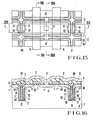
- Figs. 3A, 3B to 5 show a semiconductor memory device according to an embodiment of the present invention.
- the same reference numerals as in Figs. 3A to 5 denote the same parts as in Fig. 1.
- Fig. 3B shows a planar configuration of the semiconductor memory device, and the vertical positional relationship between the respective elements are not strictly illustrated.
- Fig. 3A is a perspective view of a semiconductor memory device according to an embodiment of the present invention.
- a region surrounded by AlAl'- A2A2'- B1B1' - B2B2' represents one memory cell MC.
- This semiconductor memory device will be described in detail with reference to Figs. 3B, 4 and 5.
- one memory cell is defined by a region MC surrounded by a broken line.
- a capacitor region CP constituting the memory cell and an element isolation region are formed around the region MC.
- a trench 12 is formed to surround each memory cell in one major surface of the semiconductor substrate 1.
- a silicon oxide film 40 serving as an element isolation film is formed in the inner surface of the trench 12, thereby isolating the adjacent memory cells.
- An n-type thin silicon film 13 is formed as one electrode of the capacitor CP on a portion (i.e., a window as part of the semiconductor substrate 11 which is not covered with the silicon oxide film 40 on the wall surfaces of the trench 12 and on the side wall of the silicon oxide film 40.
- a thin insulating film 2 such as a silicon oxide film is formed on the thin film 13.
- a thin conductive layer 3 serving as the other electrode of the capacitor CP is formed on the thin insulating film 2.
- a MIS type field effect transistor TR is formed in a region of the semiconductor substrate 1 which is surrounded by the trench.
- the transistor TR comprises n + -type diffusion layers 61 and 62 serving as drain and source or source and drain thereof, a gate insulating film 7 and a gate electrode 8 serving as one (i.e., a word iine) of memory cell selection lines formed in a matrix form.
- the n +- type diffusion layer 62 is formed on a surface portion as a window 14 of a silicon substrate 1.
- the window 14 is obtained by partially removing the silicon oxide film 40 from the side wall surface of the trench 1 2 .
- the n +- type diffusion layer 62 is electrically connected to the thin n-type silicon film as one electrode of the capacitor CP.
- n +- type diffusion layer 61 is connected through a contact hole 11 to a bit line 10 as the other type of memory cell selection lines formed in the matrix form.
- the bit line 10 is electrically insulated from the word line (the gate electrode) 8 through an insulating interlayer 9.
- the word line 8 is electrically insulated from the thin conductive layer as the other electrode of the capacitor CP through a thin insulating film 90 formed at the upper portion of the trench 12.
- the element isolation region and the capacitor are formed in the trench which is formed around each memory cell and which has a width of 1 ⁇ m or less, so that the widths of the element isolation region and the capacitor can be decreased.
- the miniaturizing and the packing density of the memory device can be greatly improved.
- the element isolation insulating film is formed on most of the inner surface of the trench, bit information interference can be prevented between the adjacent wall surfaces of the two adjacent cells.
- One electrode of the capacitor which is formed on the insulating film is directly formed on the semiconductor substrate through the window formed on the wall surface of the trench. The capacitor can therefore be electrically connected to other elements constituting the memory cell in the trench, thereby achieving a high packing density.
- the n +- type diffusion layer as the drain or source is formed on part of the side wall surfaces of the trench, the area of the n -type diffusion layer can be greatly decreased.
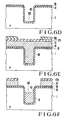
- a p-type silicon substrate having an impurity concentration of 10 15 to 10 16 cm -3 is prepared.
- the silicon oxide film 15 is formed by thermal oxidation on the p-type silicon substrate 1 to a thickness of 300 to 500 ⁇ , and a silicon nitride film 16 and a silicon oxide film 17 are respectively deposited by CVD on the silicon oxide film 15 to thicknesses of 1,000 to 1,500 A and 5,000 to 10,000 A.
- the silicon oxide film 17, the silicon nitride film 16 and the silicon oxide film 15 are sequentially etched by reactive ion etching (to be referred to as RIE hereinafter) using a photoresist pattern (not shown) as a mask and CF 4 and hydrogen gas mixture as an etchant (Fig. 6B).
- RIE reactive ion etching
- the silicon substrate 1 is etched by RIE using the films 15, 16 and 17 as masks.
- an etchant is CBrF 3 gas.
- a trench 12 is formed, as shown in Fig. 6C.
- the trench 12 has a width of 0.5 to 1 ⁇ m and a depth of about 2 to 4 ⁇ m.
- boron may be ion-implanted in the bottom of the trench to form a channel stopper CS as indicated by the broken line in Fig. 6C.
- the silicon oxide film 17 is then removed by a buffered hydrofluoric acid solution, and the exposed surface of the silicon substrate 1 may be etched by 500 ⁇ by a mixture of nitric acid and hydrofluoric acid, thereby removing the damaged layer and contamination which may be caused by RIE. Thereafter, a silicon oxide film 40 is formed by thermal oxidation on the inner surface of the 0 trench 12 to a thickness of 500 to 2,000 A (Fig. 6D). In this case, the remaining trench is designated by reference numeral 120.
- a photoresist film 18 is applied to a thickness of about 1.5 to 2 pm to bury the trench 120.
- a silicon oxide film 170 is then formed by electron cyclotron resonance (ECR) deposition method on the photoresist film 18 to a thickness of about 0.1 to 0.3 ⁇ m at a low temperature such as room temperature.
- ECR electron cyclotron resonance
- a photoresist film 180 is formed on the silicon oxide film 170 and is patterned (Fig. 6E).
- Fig. 6E is a sectional view showing the trench portion including the portion corresponding to the window 14. It should be noted that only the sectional view of the trench portion is illustrated up to Fig. 6P.
- the silicon oxide film 170 is etched by RIE using the photoresist pattern 180 as a mask and CF 4 gas as an etchant. Subsequently, the photoresist film 18 is etched by RIE using the silicon oxide pattern 170 as a mask and oxygen gas as an etchant to a depth of 0.1 to 0.8 ⁇ m from the upper end of the trench, thereby exposing partially the silicon oxide film 40 (Fig. 6F). A trench which is not associated with the formation of the window 14 is filled with the photoresist film 18.
- the exposed silicon oxide film 40 is etched using the buffered hydrofluoric acid solution to expose the silicon substrate, thereby forming a window 14 at the upper portion of the trench 120.
- the photoresist film 18 and the silicon nitride film 16 are used as masks.
- the silicon oxide film 170 and the photoresist film 18 are respectively removed by RIE using CF 4 and hydrogen gases and by an etching technique using oxygen gas (Fig. 6G).
- the trench with no window 14 is exposed such that the side wall surfaces and the bottom thereof are covered with the silicon oxide film 40.
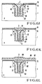
- a thin silicon film 13 doped with an n-type impurity such as phosphorus or arsenic having a concentration of 10 18 to 10 20 cm -3 is deposited by CVD to cover the entire surface of the resultant structure.
- the CVD process is performed such that silane is used as a source gas and that the silicon substrate is heated at a temperature of about 600 to 700°C, thereby forming a thin polysilicon film.
- the thin silicon film may comprise single crystalline, polycrystalline or amorphous silicon. It is essential to provide a conductive , layer which is properly connected to the n +- type diffusion layer 62 shown in Fig. 5. Therefore, silicon may be replaced with a refractory metal .(e.g., tungsten or molybdenum) or a silicide thereof.
- the thickness of the thin silicon film 13 is less than half of the width of the trench so as not to completely fill the trench 120.
- the thin silicon film 13 is etched by RIE using CBrF 3 gas, thereby leaving residual thin silicon films 13 on the side wall surfaces of the trench 120 (Fig. 6H).
- the trench with no window 14 is covered with the silicon oxide film 40 at a portion corresponding to the window 14, and any other structure is the same as described above.
- the surface of the residual thin silicon layers 13 are etched by a mixture of nitric acid and hydrofluoric acid to a thickness of 500 A.
- Thin insulating films 2 are respectively formed on the residual thin silicon layers 13 to a thickness of 50 to • 500 A (Fig. 61).
- the resultant trench is designated by reference numeral 122.
- the trench with no window 14 is covered with the silicon oxide film 40 at a portion corresponding to the window 14, and any other structure is the same as described above.
- the thin insulating film 2 comprises a silicon oxide film obtained by thermally oxidizing the thin silicon film or a two-layer structure consisting of such a silicon oxide film and a silicon nitride film obtained by CVD.
- n + -type diffusion layers 62 serving as drains or sources of the transistors TR.
- a junction depth (lateral depth) of each n +- type diffusion layer 62 is about 0.1 to 0.2 ⁇ m.
- a phosphorus-doped thin silicon film 3 as a thin conductive film is formed to a thickness which is larger than half of the width of the trench 122, thereby filling the trench 122.
- the thin silicon film 3 is etched by RIE to leave the thin silicon film 3 in only the trench 122 (Fig. 6J).
- the trench with no window 14 is covered with the silicon oxide film 40 at a portion corresponding to the window 14, and any other structure is the same as described above.
- the conditions for forming the thin silicon film 3 and the RIE conditions are the same as those of-forming the thin silicon film 13.
- the surface layer of the thin silicon film 30 is thermally oxidized to form a silicon oxide film 90 having a thickness of about 1,000 to 3,000 ⁇ (Fig. 6K).
- the trench with no window 14 is covered with the silicon oxide film 40 at a portion corresponding to the window 14, and any other structure is the same as described above.
- the trench is filled by the thin silicon film 3 which is electrically insulated by the silicon oxide film 90, the thin insulating films 2 and the silicon oxide film 40.
- the silicon film 3 is connected to the voltage supply at predetermined region.
- the silicon nitride film 16 is removed by phosphoric acid heated to a temperature of about 160°C, and the silicon oxide film 15 is removed by the buffered hydrofluoric acid solution.
- the silicon substrate 1 is thermally oxidized to form a silicon oxide film 70 (corresponding to the film 7 in Figs. 3A to 5) of 50 to 500 ⁇ thickness as a gate insulating film of the transistor.
- a phosphorus-doped thin silicon film 80 (corresponding to the film 8 in Figs. 3A to 5) is formed as a gate electrode on the gate insulating film to a thickness of 2,000 to 4,000 ⁇ .
- the thin silicon film 80 can be formed in the same manner as the thin silicon film 3.
- a silicon oxide film 92 is formed by CVD on the thin silicon film 80 to form an insulating interlayer having a thickness of 4,000 to 6,000 A (Fig. 6L).
- the trench with no window 14 is covered with the silicon oxide film 40 at a portion corresponding to the window 14, and any other structure is the same as described above.
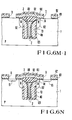
- the silicon oxide film 92 and the thin silicon film 80 are etched by RIE using a photoresist pattern (not shown) to form word lines and the contact holes 11 (Fig. 6M-1).
- a photoresist pattern not shown
- the portion corresponding to the line IV - IV of Fig. 3B is illustrated in Fig. 6M-2.
- Arsenic is ion-implanted in the exposed portions of the silicon substrate 1 through the contact holes 11 to form the n + -type diffusion layers 61 (Fig. 6N).
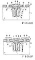
- a silicon oxide film 93 is deposited by CVD and etched to leave residual silicon oxide films 93 on only the side wall surfaces of the silicon oxide film 92 and the silicon film 80 (Fig. 60).
- Bit lines 10 are formed by a metal such as aluminum (Fig. 6P).
- Fig. 6P corresponds to Fig. 5.
- the portion shown in Fig. 6M-2 after the steps of Figs. 6N to 6P corresponds to that in Fig. 4.
- the semiconductor memory device having the structure shown in Figs. 3A to 5 is thus prepared.
- Example 2 Only the trench for forming the window 14 will be described in Example 2.
- the silicon oxide film 40 is formed by thermal oxidation on the inner wall surface of the trench 12, as shown in Fig. 6D.
- a process will be' described hereinafter wherein a silicon oxide film 41 is formed by CVD in addition to silicon oxide film 40.
- the structure shown in Fig. 6D is obtained by the method used in Example 1.
- a thickness of the silicon oxide film 40 formed by thermal oxidation can be 0 200 to 700 A which is smaller than that of the film 40 in
- a silicon oxide film 41 is then deposited by CVD on the inner wall surface of the trench and the silicon nitride film 16 to a thickness of 500 to 2,000 A (Fig. 7A).
- the silicon oxide films 40 and 41 are-etched by the buffered hydrofluoric acid solution so as to expose the silicon substrate and hence obtain the windows 14 as described in Example 1. As a result, a structure is obtained as shown in Fig. 7B.
- the CVD-SiO 2 film 41 is removed by the buffered hydrofluoric acid solution from the silicon nitride film 16 to obtain the structure which has the CVD silicon oxide film 41 laminated on the silicon oxide film 40 of the structure shown in Fig. 6J.
- the following steps are the same as those in Example 1.
- the photoresist film filled in the trench is etched to a depth corresponding to the size of each window 14 and the silicon oxide film is removed.
- the thick silicon oxide film is not preformed at a region corresponding to the window.
- the structure shown in Fig. 6B is obtained in accordance with the process of Example 1.
- the silicon substrate 1 is etched by RIE using the films 17, 16 and 15 as masks and CBrF 3 gas as etchant to form a trench 121.
- the trench 121 has a width of 0.5 to 1.0 um and a depth of about 0.2 to 0.5 U m.
- the silicon substrate surface in the trench is etched by a mixture of nitric acid and hydrofluoric acid to a depth of 500 A.
- a silicon oxide film 151 is formed by thermal oxidation to the inner surface of the trench 121 to a thickness of 300 to 500 A.
- a silicon nitride film 161 is formed on the silicon oxide film 151 to a thickness of 1,000 to 1,500 A (Fig. 8A).
- a photoresist film 18 is coated to a thickness of 1.5 to 2 ⁇ m to fill the trench 121.
- a silicon oxide film 170 having etching selectivity with respect to the photoresist film is formed by ECR deposition method on the entire surface to a thickness of 0.1 to 0.3 um.
- a photoresist film 180 is applied to the entire surface of the silicon oxide film 170 and is patterned (Fig. 8B). The opening of the photoresist pattern corresponds to a portion excluding the window 14 shown in Figs. 3A to 5. The photoresist film is not present in the trench with no window 14. It should be noted that the sectional views in Figs. 8C to 8F illustrate only trenches wherein the windows 14 are to be formed.
- the silicon oxide film 170 is etched by RIE using the photoresist pattern 180 as a mask and CF 4 gas as an etchant, and the photoresist film 18 is etched by RIE using the residual oxide film pattern 170 as a mask and oxygen gas as an etchant.
- the silicon nitride film 161 is etched by plasma etching using the photoresist film 18 as a mask (Fig. 8C). The silicon nitride film 161 in the trench with no window 14 is completely removed in the above step.
- a photoresist film having a resistance to oxygen plasma e.g., silicon-contained resist may be formed on the photoresist film 18 and may be patterned to expose portions excluding the window 141.
- the photoresist pattern may be etched by using the resultant pattern as a mask.
- the silicon nitride film 161 and the silicon oxide film 151 are removed by RIE from the bottom surface of the trench and the silicon oxide film 17.
- the silicon substrate 1 is etched by RIE using the silicon oxide film 17 and residual silicon nitride film 161 as masks and CBrF 3 as an etchant, thereby obtaining a trench 12 having a depth of 2 to 4 ⁇ m ( F ig. 8 D ).
- the silicon oxide film 151 is left on the side wall surfaces of the trench with no window 14 in this step, thereby forming a trench having a depth of 2 to 4 ⁇ m.
- a silicon oxide film 40 is formed by thermal • oxidation to a thickness of 1,000 to 3,000 A in accordance with the silicon oxide and nitride films 16 and 161 as masks (Fig. BE).
- the thick silicon oxide film is formed on the entire side wall surfaces and the bottom surface of the trench with no window 14.
- the silicon nitride film 161 and the silicon oxide film 151 are removed, the residual thin silicon films 13 and the thin insulating films 2 are formed on the side wall surfaces of the trench in accordance with the process of Example 1. Thereafter, a thin conductive film 3 is filled in the trench and is etched by RIE (Fig. 8F).
- the CVD-Si0 2 film 17 is removed by the buffered hydrofluoric acid solution, and the structure shown in Fig. 6J is obtained.
- the subsequent steps are the same as those of Example 1.
- the contact holes are formed simultaneously when the gate electrode is formed, and the n + -type diffusion regions as drains or sources are formed through the contact holes.
- the gate electrode can be self-aligned; an alignment margin between the gate electrode and the contact hole need not be provided.
- the photolithographic process is decreased by one step.
- the transistor region can be greatly decreased as compared with that of the conventional semiconductor memory device. Therefore, the area of the memory cell region can be greatly decreased to provide memory cells with a high packing density.
- Example 4 The other cell structure will be exemplified in Example 4.
- the resultant cell structure is shown in F ig. 9, and its sectional view is illustrated in Fig. 10.
- the transfer gate length is determined by precision of photolithography and gate electrode pattering. Thermal diffusion conditions and alignment errors of the contact hole 11 hardly cause errors in gate length and gate length can be easily controlled.
- the word line is formed between the n + -type diffusion layer 62 and the contact hole, so that the gate area can be decreased, thus resulting in a decrease in parasitic capacitance.
- Example 4 when the electrode 13 is a high level, a channel (an inversion layer) is formed on each side wall surface 14" of the trench in accordance with a relationship between an impurity concentration of the silicon substrate 1 and a thickness of the silicon oxide film 40. The stored charge is transferred to the bit line through the inversion layer irrespective of the ON/OFF operation of the gate electrode 8.
- an impurity concentration of the silicon substrate near the trench wall 14" must be 1 x 10 17 cm -3 or more to prevent a charge leakage from the capacitor.
- the silicon substrate 1 has the above-mentioned impurity concentration, the presence/absence of the channel stopper does not become an issue.
- the silicon substrate 1 has an impurity concentration of about 10 15 to 10 16 cm-3 since a higher impurity concentration causes a decrease in breakdown voltage of the p-n junction and the difficulty of control of a threshold voltage of the transistor.
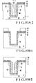
- Method (1) can be practiced by a known well formation technique. A case will be described with reference to Figs. 11A and 11B wherein method (2) is applied to Example 3.
- Fig. 11A is a sectional view of a structure including the windows 141
- Fig. 11B is a sectional view of a structure excluding the windows 141.
- a silicon oxide film 152 containing a p-type impurity such as boron is deposited on the entire surface of the resultant structure.
- the p-type impurity is diffused by annealing from the silicon oxide film 152 to the silicon substrate at the trench 12, thereby forming a p +- type layer 21.
- the p -type layer 21 is formed in the inner surface of the trench which excludes the windows 141 in Fig. 11A, and the p + -type layer 21 is formed in the entire inner surface of the trench in Fig. 11B.
- the silicon oxide film 152 is removed by the buffered hydrofluoric acid solution. The subsequent steps to that of Fig. 11E will be performed.
- Example 1 or 2 after the steps up to that of Fig. 6C are performed, a boron-doped silicon oxide film 152 is deposited and annealed to form the p +- type layer 21 (Fig. 12).
- the silicon oxide films 152 and 17 are removed by the buffered hydrofluoric acid solution, and the steps from that of Fig. 6D will be performed.
- a p-type impurity such as boron is ion-implanted in the substrate.
- This ion implantation is effectively performed by changing implantation energy levels in two or more steps. For example, when boron ions are implanted at an acceleration voltage of 50 keV and 100 keV, a p -type layer 22-can be formed to a depth of about 0.4 ⁇ m.
- the p + -type layer 22 can be formed by ion implantation and subsequent annealing to extend under the silicon oxide film 17, the silicon nitride film 16 and the silicon oxide film 15 as the masks ( F ig. 13A). For this reason, when the trench 12 is formed in the steps shown in Figs. 8A to 8D, the p +- type layers 22 are left on the upper portions of the side wall surfaces of the trench.
- Fig. 13B-1 is a sectional view of a structure including the windows 14 and Fig. 13B-2 is a sectional view of a structure excluding the windows 14.
- Still another method is proposed wherein boron is ion-implanted at an acceleration voltage of 50 keV after the structure shown in Fig. 6B is obtained.
- a trench 121 is formed, and a silicon oxide film 151 is formed in the trench 121.
- Boron is ion-implanted at an acceleration voltage of 50 keV to form a p + -type layer 23.
- the steps from that of Fig. 8A are performed.
- the p +- type layers have a high impurity concentration, their concentration is about 10 17 cm -3 which is lower than that (10 20 cm -3 or more) of the n + -type diffusion layer. No problem therefore occurs during formation of the n -type diffusion layer.
- Figs. 15, 16, 17 and 18 show a semiconductor memory device according to still another example of the present invention.
- Figs. 15 shows a horizontal positional relationship between the respective layers, and a vertical positional relationship therebetween is not strictly given in the same manner as in Fig. 3B.
- Each capacitor CP comprises a thin n-type silicon film 13 as a lower electrode formed along the inner wall surface of the trench, a thin insulating film 2 and a thin conductive film 3 serving as an upper electrode.
- a transistor TR comprises an n + -type diffusion layer 61 and 62, a gate insulating film 7, and a gate electrode 8 serving as a word line.
- the structure of the transistor TR is the same as that of the conventional one.
- the n +- type diffusion layer 63 is electrically connected to the thin n-type silicon film 13 at each window 14 through the n -type diffusion layer 62 obtained by diffusing the impurity from the thin silicon film 13.
- the n +- type diffusion layer 61 is connected to a bit line 10 through the contact hole 11, and the bit line 10 and the word line (the gate electrode) 8 are electrically insulated through an insulating interlayer 9.
- the word line 8 and the thin conductive film 3 as the upper capacitor electrode are electrically insulated through a thin insulating film 90 formed on the upper portion of the trench.
- the pair of memory cells having the common contact hole 11 are electrically isolated from other cells through a silicon oxide film formed on the inner surface of the trench 12. Charge leakage is prevented between the pair of cells by removing the thin n-type silicon film 13 at a region 14' of the trench as the boundary of the memory cells.
- FIGs. 13B-1 and 13B-2 are obtained by the method of Example 4, and the inner wall of the trench is thermally oxidized by the method of Example 3.
- Affix 1 of the figure indicates the sectional view of the structure including the windows 14, and affix 2 thereof indicates the sectional view of the structure excluding the windows 14.
- a thin silicon film 13 containing phosphorus or arsenic is deposited by the method of Example 1 and is etched by RIE to leave residual thin silicon films 13 on only the side walls of the trench 12.
- the resultant trench is designated by reference numeral 122 (Figs. 19A-1 and 19A-2).
- the pattern of photoresist film 181 is formed to expose the thin silicon films 13 at the regions 14' in accordance with the method of Example 1 or 3, as shown in Fig. 15.
- the thin silicon films 13 exposed at the regions 14' are etched by a plasma etching apparatus using CF 4 and oxygen gases.
- the length of the pattern along a direction perpendicular to the trench can be longer than the width so as to provide a larger margin for alignment with the underlayer.
- FIG. 19B-1 The sectional view of the structure including the regions 14' in this process is illustrated in Fig. 19B-1, and that without the regions 14' is illustrated in Fig. 19B - 2.
- the material may be formed to a thickness so as to completely cover the trench and the substrate, and thereafter the material may be etched back to expose the surface of the substrate.
- the pair of memory cells adjacent to each other have a common contact hole. Therefore, the resultant memory device has a higher packing density than that of the memory device shown in Figs. 3A to 6.
- the surface area of the memory cell can be greatly decreased to obtain a memory device with a high packing density.
Landscapes
- Semiconductor Memories (AREA)
- Semiconductor Integrated Circuits (AREA)
Applications Claiming Priority (4)
| Application Number | Priority Date | Filing Date | Title |
|---|---|---|---|
| JP79683/84 | 1984-04-19 | ||
| JP59079683A JPS60227461A (ja) | 1984-04-19 | 1984-04-19 | 半導体集積回路装置 |
| JP59209789A JPH0793366B2 (ja) | 1984-10-08 | 1984-10-08 | 半導体メモリおよびその製造方法 |
| JP209789/84 | 1984-10-08 |
Publications (2)
| Publication Number | Publication Date |
|---|---|
| EP0164829A1 true EP0164829A1 (de) | 1985-12-18 |
| EP0164829B1 EP0164829B1 (de) | 1988-09-28 |
Family
ID=26420692
Family Applications (1)
| Application Number | Title | Priority Date | Filing Date |
|---|---|---|---|
| EP85302116A Expired EP0164829B1 (de) | 1984-04-19 | 1985-03-26 | Halbleiterspeicherbauelement und Verfahren zur Herstellung |
Country Status (3)
| Country | Link |
|---|---|
| US (1) | US4786954A (de) |
| EP (1) | EP0164829B1 (de) |
| DE (1) | DE3565339D1 (de) |
Cited By (13)
| Publication number | Priority date | Publication date | Assignee | Title |
|---|---|---|---|---|
| EP0176254A3 (en) * | 1984-08-27 | 1986-12-30 | Kabushiki Kaisha Toshiba | Semiconductor memory device |
| EP0177066A3 (en) * | 1984-10-05 | 1987-01-28 | Nec Corporation | Semiconductor memory device with information storage vertical trench capacitor and method of manufacturing the same |
| EP0248993A1 (de) * | 1986-05-02 | 1987-12-16 | International Business Machines Corporation | Vertikal strukturierter dynamischer Speicher hoher Dichte |
| US4785337A (en) * | 1986-10-17 | 1988-11-15 | International Business Machines Corporation | Dynamic ram cell having shared trench storage capacitor with sidewall-defined bridge contacts and gate electrodes |
| AU594169B2 (en) * | 1986-07-15 | 1990-03-01 | International Business Machines Corporation | Two square memory cells |
| US4921816A (en) * | 1986-10-22 | 1990-05-01 | Oki Electric Industry Co., Ltd. | Method of making a trench dram |
| US4922313A (en) * | 1985-05-13 | 1990-05-01 | Hitachi, Ltd. | Process for manufacturing semiconductor memory device and product formed thereby |
| US4959698A (en) * | 1986-10-08 | 1990-09-25 | Mitsubishi Denki Kabushiki Kaisha | Memory cell of a semiconductor memory device |
| EP0399060A1 (de) * | 1989-05-22 | 1990-11-28 | Siemens Aktiengesellschaft | Halbleiterspeicheranordnung mit Kondensatoren mir zwei in einem Graben angeordneten Elektroden und Verfahren zu deren Herstellung |
| US4999689A (en) * | 1987-11-06 | 1991-03-12 | Sharp Kabushiki Kaisha | Semiconductor memory |
| FR2664742A1 (fr) * | 1990-07-12 | 1992-01-17 | Samsung Electronics Co Ltd | Dispositif a semi-conducteur pour memoire vive dynamique et son procede de fabrication. |
| US5422294A (en) * | 1993-05-03 | 1995-06-06 | Noble, Jr.; Wendell P. | Method of making a trench capacitor field shield with sidewall contact |
| US5843819A (en) * | 1989-05-22 | 1998-12-01 | Siemens Aktiengesellschaft | Semiconductor memory device with trench capacitor and method for the production thereof |
Families Citing this family (33)
| Publication number | Priority date | Publication date | Assignee | Title |
|---|---|---|---|---|
| KR900001836B1 (ko) * | 1985-07-02 | 1990-03-24 | 마쯔시다덴기산교 가부시기가이샤 | 반도체기억장치 및 그 제조방법 |
| JPH0797625B2 (ja) * | 1986-11-19 | 1995-10-18 | 三菱電機株式会社 | 半導体記憶装置 |
| JPS645052A (en) * | 1987-06-29 | 1989-01-10 | Mitsubishi Electric Corp | Capacitor cell of semiconductor storage device |
| US5200353A (en) * | 1987-06-29 | 1993-04-06 | Mitsubishi Denki Kabushiki Kaisha | Method of manufacturing a semiconductor device having trench capacitor |
| JPH01132176A (ja) * | 1987-11-18 | 1989-05-24 | Canon Inc | 光電変換装置 |
| US5075888A (en) * | 1988-01-09 | 1991-12-24 | Sharp Kabushiki Kaisha | Semiconductor memory device having a volatile memory device and a non-volatile memory device |
| US5140552A (en) * | 1988-02-09 | 1992-08-18 | Sharp Kabushiki Kaisha | Semiconductor memory device having a volatile memory device and a non-volatile memory device |
| JPH0821685B2 (ja) * | 1988-02-26 | 1996-03-04 | 株式会社東芝 | 半導体メモリの製造方法 |
| US4896293A (en) * | 1988-06-09 | 1990-01-23 | Texas Instruments Incorporated | Dynamic ram cell with isolated trench capacitors |
| US4958206A (en) * | 1988-06-28 | 1990-09-18 | Texas Instruments Incorporated | Diffused bit line trench capacitor dram cell |
| JPH0262073A (ja) * | 1988-08-26 | 1990-03-01 | Mitsubishi Electric Corp | 半導体記憶装置 |
| JPH07109876B2 (ja) * | 1988-09-09 | 1995-11-22 | 株式会社東芝 | 半導体記憶装置の製造方法 |
| KR910007181B1 (ko) * | 1988-09-22 | 1991-09-19 | 현대전자산업 주식회사 | Sdtas구조로 이루어진 dram셀 및 그 제조방법 |
| JPH02172253A (ja) * | 1988-12-24 | 1990-07-03 | Mitsubishi Electric Corp | 半導体装置およびその製造方法 |
| US5252845A (en) * | 1990-04-02 | 1993-10-12 | Electronics And Telecommunications Research Institute | Trench DRAM cell with vertical transistor |
| KR960006880B1 (ko) * | 1990-05-24 | 1996-05-23 | 가부시키가이샤 도시바 | 반도체 기억장치 |
| KR950008385B1 (ko) * | 1990-05-24 | 1995-07-28 | 삼성전자주식회사 | 반도체 소자의 워드라인 형성방법 |
| US5034787A (en) * | 1990-06-28 | 1991-07-23 | International Business Machines Corporation | Structure and fabrication method for a double trench memory cell device |
| US5064777A (en) * | 1990-06-28 | 1991-11-12 | International Business Machines Corporation | Fabrication method for a double trench memory cell device |
| JP3003188B2 (ja) * | 1990-09-10 | 2000-01-24 | ソニー株式会社 | 半導体メモリ及びその製造方法 |
| US5065273A (en) * | 1990-12-04 | 1991-11-12 | International Business Machines Corporation | High capacity DRAM trench capacitor and methods of fabricating same |
| JPH0541378A (ja) * | 1991-03-15 | 1993-02-19 | Mitsubishi Electric Corp | 半導体装置およびその製造方法 |
| US5156992A (en) * | 1991-06-25 | 1992-10-20 | Texas Instruments Incorporated | Process for forming poly-sheet pillar transistor DRAM cell |
| US5760452A (en) * | 1991-08-22 | 1998-06-02 | Nec Corporation | Semiconductor memory and method of fabricating the same |
| US5508541A (en) * | 1992-09-22 | 1996-04-16 | Kabushiki Kaisha Toshiba | Random access memory device with trench-type one-transistor memory cell structure |
| US5455445A (en) * | 1994-01-21 | 1995-10-03 | Kulite Semiconductor Products, Inc. | Multi-level semiconductor structures having environmentally isolated elements |
| US5557122A (en) * | 1995-05-12 | 1996-09-17 | Alliance Semiconductors Corporation | Semiconductor electrode having improved grain structure and oxide growth properties |
| US6322634B1 (en) * | 1997-01-27 | 2001-11-27 | Micron Technology, Inc. | Shallow trench isolation structure without corner exposure |
| US6168986B1 (en) * | 1998-01-23 | 2001-01-02 | Micron Technology, Inc. | Method of making a sacrificial self-aligned interconnect structure |
| US6661049B2 (en) | 2001-09-06 | 2003-12-09 | Taiwan Semiconductor Manufacturing Co., Ltd | Microelectronic capacitor structure embedded within microelectronic isolation region |
| US7262095B1 (en) * | 2005-06-07 | 2007-08-28 | Spansion Llc | System and method for reducing process-induced charging |
| US8779488B2 (en) | 2011-04-15 | 2014-07-15 | Semiconductor Energy Laboratory Co., Ltd. | Semiconductor memory device |
| KR20120121722A (ko) * | 2011-04-27 | 2012-11-06 | 에스케이하이닉스 주식회사 | 반도체 소자 및 그 형성 방법 |
Citations (2)
| Publication number | Priority date | Publication date | Assignee | Title |
|---|---|---|---|---|
| EP0010623A1 (de) * | 1978-11-03 | 1980-05-14 | International Business Machines Corporation | Verfahren zur Herstellung einer Schichtstruktur für hochintegrierte Halbleiteranordnungen mit einer zwischen zwei leitenden Schichten angeordneten Isolierschicht |
| EP0088451A1 (de) * | 1982-03-10 | 1983-09-14 | Hitachi, Ltd. | Halbleiterspeicher |
Family Cites Families (4)
| Publication number | Priority date | Publication date | Assignee | Title |
|---|---|---|---|---|
| JPS5643171A (en) * | 1979-09-17 | 1981-04-21 | Mitsubishi Electric Corp | Informing device for platform of elevator |
| US4353086A (en) * | 1980-05-07 | 1982-10-05 | Bell Telephone Laboratories, Incorporated | Silicon integrated circuits |
| JPH0666436B2 (ja) * | 1983-04-15 | 1994-08-24 | 株式会社日立製作所 | 半導体集積回路装置 |
| JPS59191374A (ja) * | 1983-04-15 | 1984-10-30 | Hitachi Ltd | 半導体集積回路装置 |
-
1985
- 1985-03-26 EP EP85302116A patent/EP0164829B1/de not_active Expired
- 1985-03-26 DE DE8585302116T patent/DE3565339D1/de not_active Expired
-
1987
- 1987-10-19 US US07/110,616 patent/US4786954A/en not_active Expired - Fee Related
Patent Citations (2)
| Publication number | Priority date | Publication date | Assignee | Title |
|---|---|---|---|---|
| EP0010623A1 (de) * | 1978-11-03 | 1980-05-14 | International Business Machines Corporation | Verfahren zur Herstellung einer Schichtstruktur für hochintegrierte Halbleiteranordnungen mit einer zwischen zwei leitenden Schichten angeordneten Isolierschicht |
| EP0088451A1 (de) * | 1982-03-10 | 1983-09-14 | Hitachi, Ltd. | Halbleiterspeicher |
Non-Patent Citations (1)
| Title |
|---|
| PATENT ABSTRACTS OF JAPAN, vol. 8, no. 63, 24th March 1984, page (E-233) (1500); & JP-A-58-213460 (NIPPON DENKI) 12-12-1983 * |
Cited By (15)
| Publication number | Priority date | Publication date | Assignee | Title |
|---|---|---|---|---|
| US5012308A (en) * | 1984-08-27 | 1991-04-30 | Kabushiki Kaisha Toshiba | Semiconductor memory device |
| EP0176254A3 (en) * | 1984-08-27 | 1986-12-30 | Kabushiki Kaisha Toshiba | Semiconductor memory device |
| EP0177066A3 (en) * | 1984-10-05 | 1987-01-28 | Nec Corporation | Semiconductor memory device with information storage vertical trench capacitor and method of manufacturing the same |
| US4922313A (en) * | 1985-05-13 | 1990-05-01 | Hitachi, Ltd. | Process for manufacturing semiconductor memory device and product formed thereby |
| EP0248993A1 (de) * | 1986-05-02 | 1987-12-16 | International Business Machines Corporation | Vertikal strukturierter dynamischer Speicher hoher Dichte |
| AU594169B2 (en) * | 1986-07-15 | 1990-03-01 | International Business Machines Corporation | Two square memory cells |
| US4959698A (en) * | 1986-10-08 | 1990-09-25 | Mitsubishi Denki Kabushiki Kaisha | Memory cell of a semiconductor memory device |
| US4785337A (en) * | 1986-10-17 | 1988-11-15 | International Business Machines Corporation | Dynamic ram cell having shared trench storage capacitor with sidewall-defined bridge contacts and gate electrodes |
| EP0264858A3 (en) * | 1986-10-17 | 1989-06-28 | International Business Machines Corporation | Dynamic ram cell having shared trench storage capacitor with sidewall-defined bridge contacts and gate electrodes |
| US4921816A (en) * | 1986-10-22 | 1990-05-01 | Oki Electric Industry Co., Ltd. | Method of making a trench dram |
| US4999689A (en) * | 1987-11-06 | 1991-03-12 | Sharp Kabushiki Kaisha | Semiconductor memory |
| EP0399060A1 (de) * | 1989-05-22 | 1990-11-28 | Siemens Aktiengesellschaft | Halbleiterspeicheranordnung mit Kondensatoren mir zwei in einem Graben angeordneten Elektroden und Verfahren zu deren Herstellung |
| US5843819A (en) * | 1989-05-22 | 1998-12-01 | Siemens Aktiengesellschaft | Semiconductor memory device with trench capacitor and method for the production thereof |
| FR2664742A1 (fr) * | 1990-07-12 | 1992-01-17 | Samsung Electronics Co Ltd | Dispositif a semi-conducteur pour memoire vive dynamique et son procede de fabrication. |
| US5422294A (en) * | 1993-05-03 | 1995-06-06 | Noble, Jr.; Wendell P. | Method of making a trench capacitor field shield with sidewall contact |
Also Published As
| Publication number | Publication date |
|---|---|
| EP0164829B1 (de) | 1988-09-28 |
| DE3565339D1 (en) | 1988-11-03 |
| US4786954A (en) | 1988-11-22 |
Similar Documents
| Publication | Publication Date | Title |
|---|---|---|
| EP0164829B1 (de) | Halbleiterspeicherbauelement und Verfahren zur Herstellung | |
| US4672410A (en) | Semiconductor memory device with trench surrounding each memory cell | |
| US4734384A (en) | Process for manufacturing semiconductor memory device | |
| EP0088922B1 (de) | Verfahren zum Herstellen von Elektroden und Verdrahtungsstreifen auf einer Halbleiteranordnung | |
| US4749661A (en) | Vertical slot bottom bipolar transistor structure | |
| US5023683A (en) | Semiconductor memory device with pillar-shaped insulating film | |
| US5214303A (en) | Semiconductor device ROM having an offset region | |
| KR900008207B1 (ko) | 반도체기억장치 | |
| US5990511A (en) | Memory cell with transfer device node in selective polysilicon | |
| EP0187596B1 (de) | Halbleiterspeichervorrichtung und Verfahren zu deren Herstellung | |
| JPH0637275A (ja) | 半導体記憶装置及びその製造方法 | |
| US5969393A (en) | Semiconductor device and method of manufacture of the same | |
| US5025295A (en) | Three-dimensional one-dimensional cell arrangement for dynamic semiconductor memories and method for the manufacture of a bit line contact | |
| US5309023A (en) | Contact structure for interconnection in semiconductor devices and manufacturing method thereof | |
| KR910007111B1 (ko) | 반도체기억장치의 제조방법 | |
| US5106774A (en) | Method of making trench type dynamic random access memory device | |
| US5432105A (en) | Method for fabricating self-aligned polysilicon contacts on FET source/drain areas | |
| US5225357A (en) | Low P+ contact resistance formation by double implant | |
| EP0009910A1 (de) | Halbleiter-Speichervorrichtung und Verfahren zum Herstellen dieser Vorrichtung | |
| EP0046857B1 (de) | Verfahren zur Herstellung einer Kontaktstruktur ohne Einfassung für Diffusionsbereiche | |
| US5216267A (en) | Stacked capacitor dynamic random access memory with a sloped lower electrode | |
| GB2233154A (en) | Manufacturing a DRAM cell semi-conductor device | |
| JPH0793368B2 (ja) | 半導体記憶装置の製造方法 | |
| US6255218B1 (en) | Semiconductor device and fabrication method thereof | |
| JPH0793366B2 (ja) | 半導体メモリおよびその製造方法 |
Legal Events
| Date | Code | Title | Description |
|---|---|---|---|
| PUAI | Public reference made under article 153(3) epc to a published international application that has entered the european phase |
Free format text: ORIGINAL CODE: 0009012 |
|
| AK | Designated contracting states |
Designated state(s): DE FR GB |
|
| 17P | Request for examination filed |
Effective date: 19860120 |
|
| 17Q | First examination report despatched |
Effective date: 19871209 |
|
| GRAA | (expected) grant |
Free format text: ORIGINAL CODE: 0009210 |
|
| AK | Designated contracting states |
Kind code of ref document: B1 Designated state(s): DE FR GB |
|
| REF | Corresponds to: |
Ref document number: 3565339 Country of ref document: DE Date of ref document: 19881103 |
|
| ET | Fr: translation filed | ||
| PLBE | No opposition filed within time limit |
Free format text: ORIGINAL CODE: 0009261 |
|
| STAA | Information on the status of an ep patent application or granted ep patent |
Free format text: STATUS: NO OPPOSITION FILED WITHIN TIME LIMIT |
|
| 26N | No opposition filed | ||
| PGFP | Annual fee paid to national office [announced via postgrant information from national office to epo] |
Ref country code: FR Payment date: 19941227 Year of fee payment: 11 |
|
| PGFP | Annual fee paid to national office [announced via postgrant information from national office to epo] |
Ref country code: GB Payment date: 19950310 Year of fee payment: 11 |
|
| PGFP | Annual fee paid to national office [announced via postgrant information from national office to epo] |
Ref country code: DE Payment date: 19950530 Year of fee payment: 11 |
|
| PG25 | Lapsed in a contracting state [announced via postgrant information from national office to epo] |
Ref country code: GB Effective date: 19960326 |
|
| GBPC | Gb: european patent ceased through non-payment of renewal fee |
Effective date: 19960326 |
|
| PG25 | Lapsed in a contracting state [announced via postgrant information from national office to epo] |
Ref country code: FR Effective date: 19961129 |
|
| PG25 | Lapsed in a contracting state [announced via postgrant information from national office to epo] |
Ref country code: DE Effective date: 19961203 |
|
| REG | Reference to a national code |
Ref country code: FR Ref legal event code: ST |