EP0165513A2 - Protection du métal de contact pour semiconducteurs - Google Patents
Protection du métal de contact pour semiconducteurs Download PDFInfo
- Publication number
- EP0165513A2 EP0165513A2 EP85106582A EP85106582A EP0165513A2 EP 0165513 A2 EP0165513 A2 EP 0165513A2 EP 85106582 A EP85106582 A EP 85106582A EP 85106582 A EP85106582 A EP 85106582A EP 0165513 A2 EP0165513 A2 EP 0165513A2
- Authority
- EP
- European Patent Office
- Prior art keywords
- metal
- contact
- photoresist
- window
- silicon
- Prior art date
- Legal status (The legal status is an assumption and is not a legal conclusion. Google has not performed a legal analysis and makes no representation as to the accuracy of the status listed.)
- Granted
Links
Images


Classifications
-
- H—ELECTRICITY
- H10—SEMICONDUCTOR DEVICES; ELECTRIC SOLID-STATE DEVICES NOT OTHERWISE PROVIDED FOR
- H10W—GENERIC PACKAGES, INTERCONNECTIONS, CONNECTORS OR OTHER CONSTRUCTIONAL DETAILS OF DEVICES COVERED BY CLASS H10
- H10W20/00—Interconnections in chips, wafers or substrates
- H10W20/40—Interconnections external to wafers or substrates, e.g. back-end-of-line [BEOL] metallisations or vias connecting to gate electrodes
- H10W20/41—Interconnections external to wafers or substrates, e.g. back-end-of-line [BEOL] metallisations or vias connecting to gate electrodes characterised by their conductive parts
- H10W20/44—Conductive materials thereof
- H10W20/4451—Semiconductor materials, e.g. polysilicon
-
- H—ELECTRICITY
- H10—SEMICONDUCTOR DEVICES; ELECTRIC SOLID-STATE DEVICES NOT OTHERWISE PROVIDED FOR
- H10P—GENERIC PROCESSES OR APPARATUS FOR THE MANUFACTURE OR TREATMENT OF DEVICES COVERED BY CLASS H10
- H10P76/00—Manufacture or treatment of masks on semiconductor bodies, e.g. by lithography or photolithography
- H10P76/20—Manufacture or treatment of masks on semiconductor bodies, e.g. by lithography or photolithography of masks comprising organic materials
- H10P76/202—Manufacture or treatment of masks on semiconductor bodies, e.g. by lithography or photolithography of masks comprising organic materials for lift-off processes
-
- H—ELECTRICITY
- H10—SEMICONDUCTOR DEVICES; ELECTRIC SOLID-STATE DEVICES NOT OTHERWISE PROVIDED FOR
- H10W—GENERIC PACKAGES, INTERCONNECTIONS, CONNECTORS OR OTHER CONSTRUCTIONAL DETAILS OF DEVICES COVERED BY CLASS H10
- H10W20/00—Interconnections in chips, wafers or substrates
- H10W20/01—Manufacture or treatment
- H10W20/031—Manufacture or treatment of conductive parts of the interconnections
- H10W20/056—Manufacture or treatment of conductive parts of the interconnections by filling conductive material into holes, grooves or trenches
-
- Y—GENERAL TAGGING OF NEW TECHNOLOGICAL DEVELOPMENTS; GENERAL TAGGING OF CROSS-SECTIONAL TECHNOLOGIES SPANNING OVER SEVERAL SECTIONS OF THE IPC; TECHNICAL SUBJECTS COVERED BY FORMER USPC CROSS-REFERENCE ART COLLECTIONS [XRACs] AND DIGESTS
- Y10—TECHNICAL SUBJECTS COVERED BY FORMER USPC
- Y10S—TECHNICAL SUBJECTS COVERED BY FORMER USPC CROSS-REFERENCE ART COLLECTIONS [XRACs] AND DIGESTS
- Y10S438/00—Semiconductor device manufacturing: process
- Y10S438/942—Masking
- Y10S438/948—Radiation resist
- Y10S438/951—Lift-off
Definitions
- the invention disclosed broadly relates to semiconductor processing and more particularly relates to metal deposition techniques in semiconductor processing.
- Alkaline developers and chemical etchants used to develop the photoresist layer for first and second metal layer depositions in existing FET processes, severely attack the contact metal, thereby producing poor inter level contacts and possibly electrical failures. Also, contaminant residues, or voids created by the reaction of the etchants with existing contact metals or semiconductor substrates, will impact reliability and life of the device structures. These residues and voids increase resistance which is a significant cause of device failure.
- a common problem with metal deposition of contact or other metal to provide interconnections in the semiconductor device is that the state-of-the-art deposition tooling deposits metal at an angle to the device wafer surface, primarily because the molten metal source is not at a "line of sight" perpendicular to the wafer surface. Therefore voids or spacing will inherently exist between the contact metal and the sides of the etched insulator.
- a protective layer is applied to the etched via hole prior to the metal deposition step. This prevents the formation of contaminant trapping voids and chemical residues which would otherwise occur at the base and/or sides of the metal subsequently deposited in the contact via hole.
- the protective layer which has a thickness of from 10 to 30 nanometers, remains intact as a permanent part of the structure.
- a photoresist lift-off process is performed for depositing metal on a semiconductor substrate or ion implanted contacts. Then, a protective film is formed over the etched via holes, prior to the metal deposition step. This prevents the formation of contaminant trapping voids and chemical residues which would otherwise occur at the base and/or sides of the metal subsequently deposited in the etched contact via hole.
- the protective film which has a thickness of from 10 to 30 nanometers, remains intact as a permanent part of the structure.
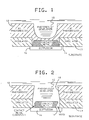
- FIGS. 1 through 3 illustrate the prior art problem.
- the developer 10 has progressed almost all the way through photoresist layer 12, providing a structure for later to be made deposition of interconnect metal but short of contacting the previously deposited contact metal 14 over the substrate or ion implanted diffused area 16.
- the developer 10 is shown to have completely removed the photoresist 12 for subsequently depositing interconnect metal over the contact 14.
- the developer 10 is now in contact with contact metal 14 at the bottom as well as the sides of via hole 18.
- FIG. 3 it is seen that the developer 10 is actually attacking the physical structure of the previously deposited contact metal 14 and corroding it thereby leaving a void 19.
- the corroded contact metal is shown to have a reduced cross-sectional area 20 which increases the resistance per unit length of the metal contact. This also presents the problem of entrapping some of the alkaline developer and/or other chemical reaction residues 22 which may present contamination problems, thereby impacting the reliability and life of the product.
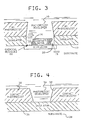
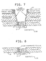
- FIGS. 4 through 9 The invention is shown in the sequence of steps illustrated in FIGS. 4 through 9.
- a contact photoresist layer 30 is shown with a via hole 32 made by a photoresist developer 34 over an insulator 36.
- the appropriate portion of the insulator is then wet or dry chemical etched to the semiconductor substrate 38 as shown in FIG. 5.
- An ion implant to produce a diffused area 37 in the semiconductor substrate can be done at this time if desired.
- a flash evaporation step is then performed. From 10 to 30 nanometers of a protective film 40, such as silicon, is flash evaporated onto the etched contact sidewalls 32. This step protects the sides of the subsequently to be deposited contact metal from attack by alkaline resist developer or other chemical etchants and thereby protects it from corrosion.
- a protective film 40 such as silicon
- contact metal 42, 44 is blanket deposited by either evaporation or sputtering onto all exposed surfaces, as is shown in FIG. 7. Referring to FIG. 8, unwanted contact metal 44 shown in FIG. 7 is lifted off and the desired remaining contact metal 42 is intact on the silicon substrate 38 or ion implant diffused region 37 in the etched region 32 of the insulator layer 36. Additional protection can be achieved by depositing an additional protective film over the interface between the metal contact and the via hole to completely seal the device by filling in the gap or void.
- interconnect metal photoresist layer 44 is applied, exposed and developed so as to expose the contact metal 42 which was previously deposited.
- the semiconductor material 38 is disclosed herein as preferably silicon, other substrate materials such as gallium arsenide and indium phosphide can also be used.
- the preferred contact metal 42 used in this invention is aluminum, other metals such as molybdenum, tungsten, titanium, and combinations of these materials can be utilized.
- the preferred photoresist 30 utilized with this invention is any positive photoresist.
- other photoresist such as optical materials, electron beam or negative photoresist, wet or dry developable, can also be used.
Landscapes
- Internal Circuitry In Semiconductor Integrated Circuit Devices (AREA)
- Electrodes Of Semiconductors (AREA)
Applications Claiming Priority (2)
| Application Number | Priority Date | Filing Date | Title |
|---|---|---|---|
| US623656 | 1984-06-22 | ||
| US06/623,656 US4640738A (en) | 1984-06-22 | 1984-06-22 | Semiconductor contact protection |
Publications (3)
| Publication Number | Publication Date |
|---|---|
| EP0165513A2 true EP0165513A2 (fr) | 1985-12-27 |
| EP0165513A3 EP0165513A3 (en) | 1987-05-13 |
| EP0165513B1 EP0165513B1 (fr) | 1991-07-24 |
Family
ID=24498919
Family Applications (1)
| Application Number | Title | Priority Date | Filing Date |
|---|---|---|---|
| EP85106582A Expired - Lifetime EP0165513B1 (fr) | 1984-06-22 | 1985-05-29 | Protection du métal de contact pour semiconducteurs |
Country Status (4)
| Country | Link |
|---|---|
| US (1) | US4640738A (fr) |
| EP (1) | EP0165513B1 (fr) |
| JP (1) | JPS618955A (fr) |
| DE (1) | DE3583544D1 (fr) |
Cited By (2)
| Publication number | Priority date | Publication date | Assignee | Title |
|---|---|---|---|---|
| EP0266522A3 (en) * | 1986-11-06 | 1988-10-05 | International Business Machines Corporation | Polyimide stud transfer process |
| EP0571108A1 (fr) * | 1992-05-06 | 1993-11-24 | STMicroelectronics, Inc. | Structure d'un trou de contact pour un dispositif semi-conducteur et son procédé de fabrication |
Families Citing this family (17)
| Publication number | Priority date | Publication date | Assignee | Title |
|---|---|---|---|---|
| US4687541A (en) * | 1986-09-22 | 1987-08-18 | Rockwell International Corporation | Dual deposition single level lift-off process |
| US5238435A (en) * | 1987-06-10 | 1993-08-24 | U.S. Philips Corporation | Liquid crystal display device and method of manufacturing such a display device |
| US5055423A (en) * | 1987-12-28 | 1991-10-08 | Texas Instruments Incorporated | Planarized selective tungsten metallization system |
| US4902379A (en) * | 1988-02-08 | 1990-02-20 | Eastman Kodak Company | UHV compatible lift-off method for patterning nobel metal silicide |
| US4956304A (en) * | 1988-04-07 | 1990-09-11 | Santa Barbara Research Center | Buried junction infrared photodetector process |
| FR2630588A1 (fr) * | 1988-04-22 | 1989-10-27 | Philips Nv | Procede pour realiser une configuration d'interconnexion sur un dispositif semiconducteur notamment un circuit a densite d'integration elevee |
| US4898841A (en) * | 1988-06-16 | 1990-02-06 | Northern Telecom Limited | Method of filling contact holes for semiconductor devices and contact structures made by that method |
| US4981816A (en) * | 1988-10-27 | 1991-01-01 | General Electric Company | MO/TI Contact to silicon |
| US4978637A (en) * | 1989-05-31 | 1990-12-18 | Sgs-Thomson Microelectronics, Inc. | Local interconnect process for integrated circuits |
| JPH03150874A (ja) * | 1989-11-07 | 1991-06-27 | Nec Corp | 半導体装置 |
| JPH03156930A (ja) * | 1989-11-15 | 1991-07-04 | Sanyo Electric Co Ltd | 半導体装置 |
| JP3086747B2 (ja) * | 1992-05-07 | 2000-09-11 | 三菱電機株式会社 | 半導体装置およびその製造方法 |
| US6130482A (en) * | 1995-09-26 | 2000-10-10 | Fujitsu Limited | Semiconductor device and method for fabricating the same |
| US6025256A (en) * | 1997-01-06 | 2000-02-15 | Electro Scientific Industries, Inc. | Laser based method and system for integrated circuit repair or reconfiguration |
| KR100770541B1 (ko) * | 2005-12-29 | 2007-10-25 | 동부일렉트로닉스 주식회사 | 반도체 소자 및 그 제조 방법 |
| TWI339444B (en) * | 2007-05-30 | 2011-03-21 | Au Optronics Corp | Conductor structure, pixel structure, and methods of forming the same |
| DE102013104953B4 (de) * | 2013-05-14 | 2023-03-02 | OSRAM Opto Semiconductors Gesellschaft mit beschränkter Haftung | Optoelektronisches Bauelement und Verfahren zu seiner Herstellung |
Family Cites Families (10)
| Publication number | Priority date | Publication date | Assignee | Title |
|---|---|---|---|---|
| US3985597A (en) * | 1975-05-01 | 1976-10-12 | International Business Machines Corporation | Process for forming passivated metal interconnection system with a planar surface |
| US4076575A (en) * | 1976-06-30 | 1978-02-28 | International Business Machines Corporation | Integrated fabrication method of forming connectors through insulative layers |
| JPS5915174B2 (ja) * | 1976-07-26 | 1984-04-07 | 日本電信電話株式会社 | フオトマスクの製造方法 |
| JPS5475275A (en) * | 1977-11-29 | 1979-06-15 | Fujitsu Ltd | Manufacture of semiconductor device |
| US4410622A (en) * | 1978-12-29 | 1983-10-18 | International Business Machines Corporation | Forming interconnections for multilevel interconnection metallurgy systems |
| US4272561A (en) * | 1979-05-29 | 1981-06-09 | International Business Machines Corporation | Hybrid process for SBD metallurgies |
| US4367119A (en) * | 1980-08-18 | 1983-01-04 | International Business Machines Corporation | Planar multi-level metal process with built-in etch stop |
| US4361599A (en) * | 1981-03-23 | 1982-11-30 | National Semiconductor Corporation | Method of forming plasma etched semiconductor contacts |
| US4377633A (en) * | 1981-08-24 | 1983-03-22 | International Business Machines Corporation | Methods of simultaneous contact and metal lithography patterning |
| US4514751A (en) * | 1982-12-23 | 1985-04-30 | International Business Machines Corporation | Compressively stresses titanium metallurgy for contacting passivated semiconductor devices |
-
1984
- 1984-06-22 US US06/623,656 patent/US4640738A/en not_active Expired - Fee Related
-
1985
- 1985-02-28 JP JP60037731A patent/JPS618955A/ja active Granted
- 1985-05-29 EP EP85106582A patent/EP0165513B1/fr not_active Expired - Lifetime
- 1985-05-29 DE DE8585106582T patent/DE3583544D1/de not_active Expired - Lifetime
Cited By (3)
| Publication number | Priority date | Publication date | Assignee | Title |
|---|---|---|---|---|
| EP0266522A3 (en) * | 1986-11-06 | 1988-10-05 | International Business Machines Corporation | Polyimide stud transfer process |
| EP0571108A1 (fr) * | 1992-05-06 | 1993-11-24 | STMicroelectronics, Inc. | Structure d'un trou de contact pour un dispositif semi-conducteur et son procédé de fabrication |
| US5317192A (en) * | 1992-05-06 | 1994-05-31 | Sgs-Thomson Microelectronics, Inc. | Semiconductor contact via structure having amorphous silicon side walls |
Also Published As
| Publication number | Publication date |
|---|---|
| JPH0312767B2 (fr) | 1991-02-21 |
| US4640738A (en) | 1987-02-03 |
| EP0165513A3 (en) | 1987-05-13 |
| EP0165513B1 (fr) | 1991-07-24 |
| DE3583544D1 (de) | 1991-08-29 |
| JPS618955A (ja) | 1986-01-16 |
Similar Documents
| Publication | Publication Date | Title |
|---|---|---|
| US4640738A (en) | Semiconductor contact protection | |
| US4267012A (en) | Process for patterning metal connections on a semiconductor structure by using a tungsten-titanium etch resistant layer | |
| US5231053A (en) | Process of forming a tri-layer titanium coating for an aluminum layer of a semiconductor device | |
| EP0100735B1 (fr) | Procédé de "lift-off" pour la fabrication de contacts autoalignés | |
| KR930005949B1 (ko) | 반도체 디바이스 제조공정 | |
| EP0523856A2 (fr) | Procédé de formation d'un via pour circuits integrés à interconnexions à multiples niveaux | |
| EP0697723A2 (fr) | Procédé de métallisation d'une couche isolante | |
| US4029562A (en) | Forming feedthrough connections for multi-level interconnections metallurgy systems | |
| CA1332323C (fr) | Methode de demoulage cryogenique du metal | |
| KR100662945B1 (ko) | 반도체 처리를 위한 상부층 이미징 리소그래피 | |
| US6645864B1 (en) | Physical vapor deposition of an amorphous silicon liner to eliminate resist poisoning | |
| US4999317A (en) | Metallization processing | |
| US5084415A (en) | Metallization processing | |
| US4847673A (en) | Semiconductor device | |
| JP2858837B2 (ja) | 半導体装置の製造方法 | |
| JP2757919B2 (ja) | 半導体装置の製造方法 | |
| KR100187677B1 (ko) | 반도체 소자의 확산방지층 형성방법 | |
| US6083823A (en) | Metal deposition process for metal lines over topography | |
| JP2892432B2 (ja) | 半導体装置の製造方法 | |
| KR100367694B1 (ko) | 반도체소자의콘택제조방법 | |
| KR100615822B1 (ko) | 반도체 소자의 파티클 제거 방법 | |
| JPS61281523A (ja) | コンタクト形成法 | |
| JPH0845811A (ja) | パターン形成方法およびそれを用いた半導体集積回路装置の製造方法 | |
| JPH02148725A (ja) | 半導体集積回路の製造方法 | |
| JPH04267337A (ja) | 半導体装置の製法 |
Legal Events
| Date | Code | Title | Description |
|---|---|---|---|
| PUAI | Public reference made under article 153(3) epc to a published international application that has entered the european phase |
Free format text: ORIGINAL CODE: 0009012 |
|
| AK | Designated contracting states |
Designated state(s): DE FR GB |
|
| 17P | Request for examination filed |
Effective date: 19860424 |
|
| PUAL | Search report despatched |
Free format text: ORIGINAL CODE: 0009013 |
|
| AK | Designated contracting states |
Kind code of ref document: A3 Designated state(s): DE FR GB |
|
| 17Q | First examination report despatched |
Effective date: 19890531 |
|
| GRAA | (expected) grant |
Free format text: ORIGINAL CODE: 0009210 |
|
| AK | Designated contracting states |
Kind code of ref document: B1 Designated state(s): DE FR GB |
|
| REF | Corresponds to: |
Ref document number: 3583544 Country of ref document: DE Date of ref document: 19910829 |
|
| ET | Fr: translation filed | ||
| PLBE | No opposition filed within time limit |
Free format text: ORIGINAL CODE: 0009261 |
|
| STAA | Information on the status of an ep patent application or granted ep patent |
Free format text: STATUS: NO OPPOSITION FILED WITHIN TIME LIMIT |
|
| 26N | No opposition filed | ||
| PGFP | Annual fee paid to national office [announced via postgrant information from national office to epo] |
Ref country code: GB Payment date: 19950413 Year of fee payment: 11 |
|
| PGFP | Annual fee paid to national office [announced via postgrant information from national office to epo] |
Ref country code: FR Payment date: 19950427 Year of fee payment: 11 |
|
| PGFP | Annual fee paid to national office [announced via postgrant information from national office to epo] |
Ref country code: DE Payment date: 19950524 Year of fee payment: 11 |
|
| PG25 | Lapsed in a contracting state [announced via postgrant information from national office to epo] |
Ref country code: GB Effective date: 19960529 |
|
| GBPC | Gb: european patent ceased through non-payment of renewal fee |
Effective date: 19960529 |
|
| PG25 | Lapsed in a contracting state [announced via postgrant information from national office to epo] |
Ref country code: FR Effective date: 19970131 |
|
| PG25 | Lapsed in a contracting state [announced via postgrant information from national office to epo] |
Ref country code: DE Effective date: 19970201 |
|
| REG | Reference to a national code |
Ref country code: FR Ref legal event code: ST |