EP0173558A2 - Halbleiterverbindung enthaltende Mesastruktur - Google Patents
Halbleiterverbindung enthaltende Mesastruktur Download PDFInfo
- Publication number
- EP0173558A2 EP0173558A2 EP85306086A EP85306086A EP0173558A2 EP 0173558 A2 EP0173558 A2 EP 0173558A2 EP 85306086 A EP85306086 A EP 85306086A EP 85306086 A EP85306086 A EP 85306086A EP 0173558 A2 EP0173558 A2 EP 0173558A2
- Authority
- EP
- European Patent Office
- Prior art keywords
- mesa structure
- mesa
- etching
- plane
- compound semiconductor
- Prior art date
- Legal status (The legal status is an assumption and is not a legal conclusion. Google has not performed a legal analysis and makes no representation as to the accuracy of the status listed.)
- Withdrawn
Links
Images


Classifications
-
- H—ELECTRICITY
- H10—SEMICONDUCTOR DEVICES; ELECTRIC SOLID-STATE DEVICES NOT OTHERWISE PROVIDED FOR
- H10D—INORGANIC ELECTRIC SEMICONDUCTOR DEVICES
- H10D62/00—Semiconductor bodies, or regions thereof, of devices having potential barriers
- H10D62/10—Shapes, relative sizes or dispositions of the regions of the semiconductor bodies; Shapes of the semiconductor bodies
- H10D62/117—Shapes of semiconductor bodies
-
- H—ELECTRICITY
- H10—SEMICONDUCTOR DEVICES; ELECTRIC SOLID-STATE DEVICES NOT OTHERWISE PROVIDED FOR
- H10D—INORGANIC ELECTRIC SEMICONDUCTOR DEVICES
- H10D62/00—Semiconductor bodies, or regions thereof, of devices having potential barriers
- H10D62/40—Crystalline structures
- H10D62/405—Orientations of crystalline planes
-
- H—ELECTRICITY
- H10—SEMICONDUCTOR DEVICES; ELECTRIC SOLID-STATE DEVICES NOT OTHERWISE PROVIDED FOR
- H10P—GENERIC PROCESSES OR APPARATUS FOR THE MANUFACTURE OR TREATMENT OF DEVICES COVERED BY CLASS H10
- H10P50/00—Etching of wafers, substrates or parts of devices
- H10P50/60—Wet etching
- H10P50/64—Wet etching of semiconductor materials
- H10P50/642—Chemical etching
- H10P50/646—Chemical etching of Group III-V materials
- H10P50/648—Anisotropic liquid etching
Definitions
- This invention relates to a mesa structure comprising a compound semiconductor, particularly, composed of GaAs/GaAlAs type material.
- a mesa structure is extremely valuable for use in the production of semiconductor devices composed of GaAs/GaAlAs type material.
- etching speed differs depending on the direction of the plane of crystal to be etched. Accordingly, this results in a drawback that while a forward mesa structure having a slope with an angle of greater than 90 degree between the bottom face and the side face upon mesa etching is formed along a certain direction, a reversed mesa structure having an overhang shape with an angle of equal to or less than 90 degree between the bottom face and the side face upon mesa etching is formed in the direction perpendicular to the above-mentioned direction.
- This invention provides an advantageous mesa structure having a single layer (including that of single crystal) or plural layers composed of a compound semiconductor, particularly of Ga 1-x Al x As (0 ⁇ x ⁇ 1), in which all of the sloped surfaces of the mesa structure are inclined outwardly from the top surface of the mesa structure.
- the surface at the top of the mesa structure is hereinafter referred to as the top face.
- the above-mentioned mesa structure can be obtained by etching the (100) plane of the crystal with the mixed solution of NH 4 0H, H 2 0 2 and H 2 0 by way of a desired mask. In this case, conditioning of the etching solution is important.
- the (100) plane is ordinarily used for the device.
- the production of a mesa structure using the (100) plane as the main surface will now be explained.
- a GaAs wafer 1 having the main surface at the (100) plane is prepared and an etching mask 2 having a plane pattern as shown in Figure 1 is formed on the main surface.
- An etching mask with square apertures of 1 mm side is prepared by depositing a SiO 2 film of 0.3 ⁇ m thickness at 400°C using a well-known CVD process (Chemical Vapor Deposition process).
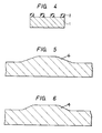
- Figure 4 is a cross sectional view showing this state.
- one side is aligned in parallel with the cleavage direction of the GaAs wafer.
- the GaAs wafer having the thus formed square Si0 2 mask is etched by using an etching solution comprising the composition as described below.
- composition and the method of preparing the etching solution is as follows:
- [H 2 0 2 ] as described above means a commercial 30% (by volume) aqueous solution of H 2 0 2 , so that the solution has the composition 0.177N NH 4 OH : 0.0476N H 2 0 2 (3.72 : 1).
- the purpose of this process can equally be attained by incorporating [H 2 0 2 ] within a range from 5 cc to 25 cc to the entire 100 cc volume, giving a range of compositions of the etching solution of 0.177N NH 4 OH : 0.0117 to 0.0548N H 2 0 2 , i.e. in the range 14.5 : 1 to 3.22 : 1.
- Figures 5 and 6 are views showing the cross sectional mesa structures obtained by use of such solutions using a GaAs wafer having a direction of plane (100).
- Figure 5 is an etching cross section in the direction of (110) plane, that is, the cross section through a mesa 4 in the conventional forward mesa direction
- Figure 6 is an etching cross section in the direction (110) plane, that is, the cross section of a so-called conventional reversed mesa direction, each of which shows forward mesa structures.
- the angle relative to the wafer surface is about 18 degrees in the direction of the (110) plane and about 25 degree in the direction of the (110) plane.
- the mesa structure according to this invention is applied to the operation region of a field effect transistor.
- the mesa structure according to this invention is also applicable to LED, LD or like other device in addition to the field effect transistor.
- FIG. 7 shows a GaAs FET (field effect transistor) prepared by using the mesa structure according to this invention.
- This FET comprises a wafer 3 having an operation layer doped with - 2 x 10 17 cm -3 Te epitaxially grown to a thickness of 0. 5 ⁇ m on a semi-insulating GaAs substrate.
- This FET is prepared by the steps as described below. (1) The epitaxial grown layer at the operating region portion of the FET is etched into a mesa configuration 4 for the inter-device separation.
- Ohmic electrodes 5, 6 each composed of Au/Ni/AuGe are formed by the tecnics of photoetching, vapor deposition and alloying. A pair of electrodes 5, 6 form a source and a drain. (3) In the same manner, a gate electrode 8 is prepared by using photoetching and vapor deposition-tecnics.
- the mesa structure is formed by using the NH 4 OH type etching solution as described above. Since each of the portions of the FET can be prepared by the known steps employed so far,except for forming the operation region of the FET into the mesa structure 4, explanations for the details of the preparation steps are omitted. Since the requirement for previously determining the aligning direction either to (110) or (110) in the photolithography can thus be eliminated, as well as the work for confirming the aligning direction, i. e., the work for confirming that the gate lead out portion 7 is always in the forward mesa direction is no more necessary, the working steps can be shortened and occurrence of defects due to the erroneous aligning in the direction can completely be eliminated.
Landscapes
- Weting (AREA)
- Junction Field-Effect Transistors (AREA)
- Drying Of Semiconductors (AREA)
- Electrodes Of Semiconductors (AREA)
Applications Claiming Priority (2)
| Application Number | Priority Date | Filing Date | Title |
|---|---|---|---|
| JP59178315A JPS6158273A (ja) | 1984-08-29 | 1984-08-29 | 化合物半導体メサ状構造体 |
| JP178315/84 | 1984-08-29 |
Publications (2)
| Publication Number | Publication Date |
|---|---|
| EP0173558A2 true EP0173558A2 (de) | 1986-03-05 |
| EP0173558A3 EP0173558A3 (de) | 1987-10-07 |
Family
ID=16046326
Family Applications (1)
| Application Number | Title | Priority Date | Filing Date |
|---|---|---|---|
| EP85306086A Withdrawn EP0173558A3 (de) | 1984-08-29 | 1985-08-28 | Halbleiterverbindung enthaltende Mesastruktur |
Country Status (3)
| Country | Link |
|---|---|
| EP (1) | EP0173558A3 (de) |
| JP (1) | JPS6158273A (de) |
| KR (1) | KR860002136A (de) |
Cited By (1)
| Publication number | Priority date | Publication date | Assignee | Title |
|---|---|---|---|---|
| DE4427840A1 (de) * | 1994-07-28 | 1996-02-01 | Osa Elektronik Gmbh | Verfahren zur Effizienzerhöhung von A¶I¶¶I¶¶I¶B¶V¶ - Halbleiter-Chips |
Family Cites Families (3)
| Publication number | Priority date | Publication date | Assignee | Title |
|---|---|---|---|---|
| FR2168936B1 (de) * | 1972-01-27 | 1977-04-01 | Labo Electronique Physique | |
| FR2486104A1 (fr) * | 1980-07-04 | 1982-01-08 | Radiotechnique Compelec | Procede d'obtention de creusures a contour circulaire dans les monocristaux de composes intermetalliques cristallisant dans le systeme cubique a faces centrees et dispositif comportant de telles creusures |
| DE3678761D1 (de) * | 1985-07-15 | 1991-05-23 | Philips Nv | Verfahren zur herstellung einer halbleiteranordnung unter verwendung des aetzens einer ga-as-schicht mittels einer alkalischen loesung von wasserstoffperoxide. |
-
1984
- 1984-08-29 JP JP59178315A patent/JPS6158273A/ja active Pending
-
1985
- 1985-08-12 KR KR1019850005790A patent/KR860002136A/ko not_active Withdrawn
- 1985-08-28 EP EP85306086A patent/EP0173558A3/de not_active Withdrawn
Cited By (1)
| Publication number | Priority date | Publication date | Assignee | Title |
|---|---|---|---|---|
| DE4427840A1 (de) * | 1994-07-28 | 1996-02-01 | Osa Elektronik Gmbh | Verfahren zur Effizienzerhöhung von A¶I¶¶I¶¶I¶B¶V¶ - Halbleiter-Chips |
Also Published As
| Publication number | Publication date |
|---|---|
| JPS6158273A (ja) | 1986-03-25 |
| KR860002136A (ko) | 1986-03-26 |
| EP0173558A3 (de) | 1987-10-07 |
Similar Documents
| Publication | Publication Date | Title |
|---|---|---|
| US4262296A (en) | Vertical field effect transistor with improved gate and channel structure | |
| EP0551110B1 (de) | Verbindungshalbleiterbauelemente | |
| US7294201B2 (en) | Method of manufacturing crystal of III-V compound of the nitride system, crystal substrate of III-V compound of the nitride system, crystal film of III-V compound of the nitride system, and method of manufacturing device | |
| US5242839A (en) | Method of manufacturing an integrated photoelectric receiving device | |
| US4751195A (en) | Method of manufacturing a heterojunction bipolar transistor | |
| US4496403A (en) | Method of making a compound semiconductor laser | |
| US4524376A (en) | Corrugated semiconductor device | |
| US6784064B2 (en) | Heterojunction bipolar transistor and method of making heterojunction bipolar transistor | |
| US6168962B1 (en) | Method of manufacturing a semiconductor light emitting device | |
| EP0274866B1 (de) | Verfahren zum Herstellen eines Feldeffekttransistors mit selbstausrichtendem Gatter | |
| US20020117665A1 (en) | Bipolar transistor | |
| EP0289343B1 (de) | Heteroübergang-Bipolartransistor | |
| JPS61199666A (ja) | 電界効果トランジスタ | |
| JP3057679B2 (ja) | ヘテロ接合バイポーラトランジスタ及びその製造方法 | |
| JPS6158273A (ja) | 化合物半導体メサ状構造体 | |
| JPH01248524A (ja) | 半導体装置とその製造方法 | |
| JPS60229375A (ja) | 化合物半導体装置の製法 | |
| CA2057123C (en) | Semiconductor device and method of making it | |
| US5273807A (en) | Substrate having a V-shaped groove of a special configuration in a substrate | |
| JPH02306668A (ja) | 量子細線を有する半導体装置及びその製造方法 | |
| JPH0964063A (ja) | 砒化ガリウム半導体素子 | |
| JP2615657B2 (ja) | ヘテロ接合バイポーラトランジスタ | |
| JPH03129833A (ja) | 半導体装置の製造方法 | |
| JPS6065577A (ja) | 極めて短いゲ−ト及び水平構造を有する電界効果トランジスタ及びその製造方法 | |
| JPS6211236A (ja) | 化合物半導体の化学エツチング方法 |
Legal Events
| Date | Code | Title | Description |
|---|---|---|---|
| PUAI | Public reference made under article 153(3) epc to a published international application that has entered the european phase |
Free format text: ORIGINAL CODE: 0009012 |
|
| 17P | Request for examination filed |
Effective date: 19851011 |
|
| AK | Designated contracting states |
Kind code of ref document: A2 Designated state(s): DE FR GB |
|
| PUAL | Search report despatched |
Free format text: ORIGINAL CODE: 0009013 |
|
| RHK1 | Main classification (correction) |
Ipc: H01L 21/30 |
|
| AK | Designated contracting states |
Kind code of ref document: A3 Designated state(s): DE FR GB |
|
| STAA | Information on the status of an ep patent application or granted ep patent |
Free format text: STATUS: THE APPLICATION IS DEEMED TO BE WITHDRAWN |
|
| 18D | Application deemed to be withdrawn |
Effective date: 19880408 |
|
| RIN1 | Information on inventor provided before grant (corrected) |
Inventor name: MORIOKA, MAKOTO Inventor name: USAGAWA, TOSHIYUKI Inventor name: SHIRAKI, YASUHIRO Inventor name: KATAYAMA, YOSHIFUMI Inventor name: MORI, MITSUHIRO |