EP0173965A2 - Leistungssteuerungsvorrichtung für Plattengerät - Google Patents
Leistungssteuerungsvorrichtung für Plattengerät Download PDFInfo
- Publication number
- EP0173965A2 EP0173965A2 EP85110890A EP85110890A EP0173965A2 EP 0173965 A2 EP0173965 A2 EP 0173965A2 EP 85110890 A EP85110890 A EP 85110890A EP 85110890 A EP85110890 A EP 85110890A EP 0173965 A2 EP0173965 A2 EP 0173965A2
- Authority
- EP
- European Patent Office
- Prior art keywords
- supplied
- read
- signal
- power
- write
- Prior art date
- Legal status (The legal status is an assumption and is not a legal conclusion. Google has not performed a legal analysis and makes no representation as to the accuracy of the status listed.)
- Granted
Links
Images



Classifications
-
- G—PHYSICS
- G11—INFORMATION STORAGE
- G11B—INFORMATION STORAGE BASED ON RELATIVE MOVEMENT BETWEEN RECORD CARRIER AND TRANSDUCER
- G11B19/00—Driving, starting, stopping record carriers not specifically of filamentary or web form, or of supports therefor; Control thereof; Control of operating function ; Driving both disc and head
- G11B19/20—Driving; Starting; Stopping; Control thereof
-
- G—PHYSICS
- G11—INFORMATION STORAGE
- G11B—INFORMATION STORAGE BASED ON RELATIVE MOVEMENT BETWEEN RECORD CARRIER AND TRANSDUCER
- G11B19/00—Driving, starting, stopping record carriers not specifically of filamentary or web form, or of supports therefor; Control thereof; Control of operating function ; Driving both disc and head
-
- G—PHYSICS
- G11—INFORMATION STORAGE
- G11B—INFORMATION STORAGE BASED ON RELATIVE MOVEMENT BETWEEN RECORD CARRIER AND TRANSDUCER
- G11B19/00—Driving, starting, stopping record carriers not specifically of filamentary or web form, or of supports therefor; Control thereof; Control of operating function ; Driving both disc and head
- G11B19/02—Control of operating function, e.g. switching from recording to reproducing
-
- G—PHYSICS
- G11—INFORMATION STORAGE
- G11B—INFORMATION STORAGE BASED ON RELATIVE MOVEMENT BETWEEN RECORD CARRIER AND TRANSDUCER
- G11B5/00—Recording by magnetisation or demagnetisation of a record carrier; Reproducing by magnetic means; Record carriers therefor
- G11B5/48—Disposition or mounting of heads or head supports relative to record carriers ; arrangements of heads, e.g. for scanning the record carrier to increase the relative speed
- G11B5/54—Disposition or mounting of heads or head supports relative to record carriers ; arrangements of heads, e.g. for scanning the record carrier to increase the relative speed with provision for moving the head into or out of its operative position or across tracks
- G11B5/55—Track change, selection or acquisition by displacement of the head
- G11B5/5521—Track change, selection or acquisition by displacement of the head across disk tracks
- G11B5/5526—Control therefor; circuits, track configurations or relative disposition of servo-information transducers and servo-information tracks for control thereof
- G11B5/553—Details
Definitions
- the present invention relates to a disk apparatus with low power consumption.
- a conventional disk apparatus e.g., a floppy disk system is illustrated in Fig. 1.
- Floppy disk drivers 5 and 7 for driving the floppy disk drive are connected to a floppy disk controller 3 and a main processor 1 through a floppy disk interface (not shown).
- the controller 3 controls the drivers 5 and 7 under the control of the processor 1 to perform data read/write access, serial/parallel conversion and CRC (Cyclic Redundancy Check).
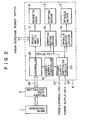
- Fig. 2 is a detailed block diagram of a conventional floppy disk driver 5.
- the driver 5 has a magnetic head 9, a read/write amp 11 for supplying a read/write signal to the head 9, a stepping motor 13 for driving a carriage having the head 9 thereon, a stepping motor driver 15, a spindle motor 17 for driving the floppy disk, a spindle motor driver 19, a power supply controller 21, a power supply switching circuit 23 and a controller 25 for controlling the above- mentioned components 11, 15, 19 and 21.
- the controller 25 controls the overall operation of the driver 5 in response to an interface signal supplied from the controller 3.
- the controller 25 comprises a random logic circuit constituted by TTL gates or a microprocessor controlled by a program.
- the controller 25 is connected to the controller 21.
- the controller 21 is connected to the circuit 23.
- the controller 21 controls power supply switching of the circuit 23.
- the circuit 23 supplies a plurality of power supply voltages 27 externally supplied under the control of the controller 21 to or stops supplying them to the driver 15, the motor 13, the driver 19 and the motor 17. At the same time, the circuit 23 switches different types of power supply voltages (e.g., +5 V and +12 V).
- the circuit 23 supplies the power supply voltage to the driver 19 and the motor 17 or stops supplying it thereto.
- the circuit 23 supplies the power supply voltage to the driver 15 and the motor 13 or stops supplying it thereto, and switches the different types of power supply voltages applied to the driver 15 and the motor 13.
- the selection of the power supply voltage applied to the driver 15 and the motor 13 by the circuit 23 is performed such that a DC +12 V voltage is applied to the driver 15 and the motor 13 when the motor 13 requires a high torque, but a DC +5 V voltage is supplied thereto when the motor 13 requires a low torque.
- the amp 11 directly receives the externally applied power supply voltage.
- MOTORON signal is used as one of interface signals 29.
- the processor 1 can directly control driving of the motor 17 in response to the MOTORON signal.
- the controller 25 directly controls the controller 21, and the power supply voltage 27 is supplied from the circuit 23 to the driver 19 and the motor 17.
- the power supply voltage is not supplied from the circuit 23 to the driver 19 and the motor 17.
- the processor 1 does not use the driver 5
- the power supply voltage is not supplied to the driver 19 and the motor 17, thereby achieving lower power dissipation and hence decreasing heat dissipation.
- the two types of power supply voltages are selectively applied to the motor 13 in accordance with the operating mode.
- a high torque is required, so that the motor 13 receives a high voltage (i.e., 12-V).
- a period of time (generally called a "settling time") required for application of the high voltage is started when the head receives a seek instruction from the processor 1 and starts a seek operation (i.e., after a STEP PULSE as one of the interface signals is received) and is ended when the seek instruction is completely executed and the stepping motor is completely stopped.
- the processor 1 When the processor 1 does not use the driver 5 and is held in the wait mode, the power supply voltage is not supplied to the driver 15 and the motor 13, thereby achieving low power consumption and decreasing heat generation.
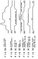
- Figs. 3A through 3G are are timing charts of signals for explaining the power consumption state of the driver 5.
- Fig. 3A shows a change in total power dissipation
- Fig. 3B shows an application state of the external power supply voltage
- Fig. 3C shows a state of the MOTORON signal
- Fig. 3D shows a seek operation
- Fig. 3E shows a state of the power supply voltage applied to the motor 13
- Fig. 3F shows a state of power consumption in the motor 17
- Fig. 3G shows a state of the power supply voltage applied to the amp 11.
- the power supply voltage 27 is always applied to the amp 11 irrespective of the operation mode of the driver 5, so that the amp 11 always consumes power and radiates heat.
- the voltage 27 is applied to the amp 11 when the motor 17 is started and while the seek operation is being performed. As a result, high power is consumed.
- a floppy disk apparatus comprising:
- the power supply voltage is not supplied to the read/write amp 11 except for a necessary period of time, thereby decreasing power consumption.
- a peak of the total power consumption can be eliminated, and the power consumption of the overall system can be averaged. As a result, heat generation can be decreased as a whole.
- Fig. 4 is a block diagram of a floppy disk driver 30 according to an embodiment of the present invention.
- the driver 30 is controlled by a floppy disk interface signal 29 supplied from a floppy disk controller 3 under the control of a main processor 1.
- a read/write amp 11 amplifies read and write signals with respect to a magnetic head 9.
- a stepping motor 13 drives a carriage having the head 9 thereon.
- the motor 13 is driven by a stepping motor driver 15.
- a spindle motor 17 drives the floppy disk.
- the motor 17 is driven by a spindle motor driver 19.
- a controller 31 controls the overall operation of the driver 30.
- a power supply switching circuit 23 supplies +5 and +12 V power supply voltages 27 (when the driver 5 is incorporated in a personal computer system, for example, these voltages are those from the personal computer) externally supplied under the control of the controller 21 to or stops supplying them to the driver 15, the motor 13, the driver 19 and the motor 17.
- the circuit 23 switches different types of power supply voltages (e.g., +5 V and +12 V).
- the circuit 23 supplies the power supply voltage to the driver 19 and the motor 17 or stops supplying it thereto.
- the circuit 23 supplies the power supply voltage to the driver 15 and the motor 13 or stops supplying it thereto, and switches the different types of power supply voltages applied to the driver 15 and the motor 13.
- the selection of the-power supply voltage applied to the driver 15 and the motor 13 by the circuit 23 is performed such that a DC +12 V voltage is applied to the driver 15 and the motor 13 when the motor 13 requires a high torque, but a DC +5 V voltage is supplied thereto when the motor 13 requires a low torque.
- the controller 31 exchanges interface signals 29 with the controller 3 to perform decoding and execution of an instruction from the processor 1, a status acknowledgement to the processor 1, reception/transmission of data with respect to the amp 11, sending of the read/write instruction, start/stop control of the driver 19 for controlling the motor 17, and excitation phase control of the driver 15 for controlling the motor 13. In this manner, the controller 31 performs control of the overall system.
- the controller 31 comprises a random logic circuit of TTL gates or the like. However, the controller 31 may comprise a microprocessor controlled by a program.
- the power supply controller 21 controls the power supply switching circuit 23 under the control of the controller 31.
- the controller 21 causes the circuit 23 to supply a high voltage (DC +12 V) to the motor 13 while the head 9 performs a seek.
- the controller 21 causes the circuit 23 to apply a low voltage (DC +5 V) to the motor 13.
- a power supply controller 33 controls operation of a power supply switching circuit 35 under the control of the controller 31.
- the circuit 35 selectively supplies the power supply voltages 27 under the control of the controller 33.
- Figs. 5A through 5G show the power dissipation state of the driver 30 shown in Fig. 4, in which Fig. 5A shows a change in total power dissipation, Fig. 5B shows a state of an application of the external power supply voltage 27, Fig. 5C shows a state of the MOTORON signal, Fig. 5D shows a state of seek, Fig. 5E shows a state of a power supply voltage applied to the stepping motor, Fig. 5F shows a state of power dissipation in the spindle motor, and Fig. 5G shows a state of the power supply voltage applied to the read/write amp 11.
- Fig. 6 is a detailed circuit diagram of the controller 31 shown in Fig. 4.
- a step signal STEP and a drive select signal DRIVE SELECT are supplied from the controller 3 to a 2-negative input AND gate 37.
- An output from the AND gate 37 is supplied to a stepping motor phase controller 39 and a first flip-flop 41.
- the controller 39 also receives a DIRECTION signal representing a rotational direction.
- the controller 39 supplies two phase signals ⁇ A and ⁇ B to the driver 15.
- the driver 15 supplies two phase signals to the motor 13 through A and B coils.
- the flip-flop 41 latches the output signal from the AND gate 37.
- the flip-flop 41 comprises a monostable multivibrator.
- a Q output signal from the flip-flop 41 is supplied to the circuit 23.
- the circuit 23 controls the power supply voltage supplied to the drivers 15 and 19.
- the signal MOTORON is supplied to a second flip-flop 43.
- the flip-flop 43 comprises a monostable multivibrat
- Q outputs from the flip-flops 41 and 43 and the MOTORON signal are supplied to a NOR gate 45.
- An output from the NOR gate 45 is supplied to the bases of first and second transistors Ql and Q2 serving as switches.
- the emitters of the transistors Ql and Q2 are commonly grounded.
- the collector terminals of the transistors Ql and Q2 are connected to the bases of transistors Q3 and Q4 through resistors, respectively.
- a voltage of +12 V is applied to the emitter of the transistor Q3, and a voltage of +5 V is applied to the emitter of the transistor Q4.
- the collectors of the transistors Q3 and Q4 are connected to the amp 11.
- the portion surrounded by the broken line is a peripheral LSI chip,model No. T6677S available from TOSHIBA CORPORATION, Japan.
- the data read/write access with respect to the head 9 is performed when the following two conditions are satisfied:
- a rush current during starting of the motor 17 and high-voltage supply to the motor 13 causes a peak in total power dissipation.
- the circuit 35 stops supplying the power supply voltage 27 to the amp 11 for a predetermined period of time until the rush current disappears after the motor 17 is started, during the seek of the head 9, and until a predetermined period of time has elapsed after the final step pulse is supplied from the processor 1 to drive the motor 13.
- the output of low level (Fig. 7E) is supplied from the NOR gate 45 to the bases of the transistors Ql and Q2.
- the base potentials of the transistors Ql and Q2 are set at 0 V, as shown in Fig. 7F.
- the transistors Ql and Q2 are kept off.
- the transistors Q3 and Q4 are also kept off.
- the voltages of +12 V and +5 V shown in Figs. 7G and 7H are not supplied to the amp 11.
- the controller 3 generates the MOTORON signal as shown in Fig.
- the MOTORON signal is significant and is set at low level, as shown in Fig. 7A.
- the MOTORON signal is latched by the flip-flop 43, as shown in Fig. 7D.
- the Q output of high level from the flip-flop 43 is supplied to one input terminal of the NOR gate 45.
- the NOR gate 45 supplies the low level signal (Fig. 7 E ) to the bases of the transistors Ql and Q2.
- the base potentials of the transistors Ql and Q2 are set at 0 V, as shown in Fig. 7F, and the transistors are kept off.
- the transistors Q3 and Q4 are also kept off. Therefore, the voltages of +12 V and +5 V are not supplied to the amp 11, as shown in Figs. 7G and 7H.
- the Q output from the flip-flop 43 is disabled when a predetermined period of time (i.e., time Tl) has elapsed.
- the Q output of low level from the flip-flop 41 and the Q output of low level from the flip-flop 43 are supplied to the NOR gate 45.
- the NOR gate 45 generates a signal of high level, as shown in Fig. 7E.
- the bases of the transistors Ql and Q2 receive the signals of high level, as shown in Fig. 7F.
- the transistors Ql and Q2 are turned on, and the voltages of +12 V and +5 V are supplied to the amp 11, as shown in Figs. 7G and 7H, respectively.
- the controller 3 performs the seek operation in response to the seek instruction from the processor 1, and the STEP signal (Fig. 7B) and the DRIVE SELECT signal are supplied to the AND gate 37.
- the output from the AND gate 37 is latched by the flip-flop 41, as shown in Fig. 7C.
- the Q output of high level from the flip-flop 41 and the Q output of low level from tranflip-flop 43 are simultaneously supplied to the NOR gate 45.
- the signal of low level is supplied from the NOR gate 45 to the bases of the transistors Ql and Q2, the transistors Ql and Q2 are kept off, and the transistors Q3 and Q4 are also kept off. Therefore, the voltages of +12 V and +5 V are not supplied to the amp 11 in the same manner as described above.
- a period of time T2 until the Q output from the flip-flop 41 falls in response to the final step pulse after an input T to the flip-flop 41 is hit by a trigger signal from the AND gate 37 and an output signal then rises is designed to be longer than the step pulse width T 3 of Fig. 7B. With such a design, the power supply voltage 27 can be continuously cut off from the amp 11 during the seek operation.
- the above embodiment exemplifies the floppy disk driver.
- the present invention is not limited to this.
- the present invention can be applied to a hard disk driver or an optical disk driver.
Landscapes
- Moving Of Head For Track Selection And Changing (AREA)
- Power Sources (AREA)
Applications Claiming Priority (2)
| Application Number | Priority Date | Filing Date | Title |
|---|---|---|---|
| JP59183862A JPS6163965A (ja) | 1984-09-04 | 1984-09-04 | フロツピ−デイスク装置 |
| JP183862/84 | 1984-09-04 |
Publications (3)
| Publication Number | Publication Date |
|---|---|
| EP0173965A2 true EP0173965A2 (de) | 1986-03-12 |
| EP0173965A3 EP0173965A3 (en) | 1988-06-08 |
| EP0173965B1 EP0173965B1 (de) | 1991-05-15 |
Family
ID=16143122
Family Applications (1)
| Application Number | Title | Priority Date | Filing Date |
|---|---|---|---|
| EP85110890A Expired EP0173965B1 (de) | 1984-09-04 | 1985-08-29 | Leistungssteuerungsvorrichtung für Plattengerät |
Country Status (4)
| Country | Link |
|---|---|
| US (1) | US4709279A (de) |
| EP (1) | EP0173965B1 (de) |
| JP (1) | JPS6163965A (de) |
| DE (1) | DE3582836D1 (de) |
Cited By (4)
| Publication number | Priority date | Publication date | Assignee | Title |
|---|---|---|---|---|
| EP0400923A3 (de) * | 1989-06-02 | 1991-10-09 | Fujitsu Limited | Plattenantriebsvorrichtung und Verfahren zu deren Steuerung |
| EP0381519A3 (de) * | 1989-02-03 | 1992-02-26 | Seagate Technology International | Kompensierung der Schrittmotor-Drehmoment-Veränderung mit verstellbarer Spannung |
| EP0356763A3 (de) * | 1988-08-30 | 1992-05-13 | Kabushiki Kaisha Toshiba | Gerät und Verfahren mit geringem Energieverbrauch zum Zugriff auf einen Aufzeichnungsträger |
| US5243691A (en) * | 1986-06-18 | 1993-09-07 | Hitachi, Ltd. | System for printing documents |
Families Citing this family (9)
| Publication number | Priority date | Publication date | Assignee | Title |
|---|---|---|---|---|
| JPS63157856U (de) * | 1987-04-01 | 1988-10-17 | ||
| JP2814242B2 (ja) * | 1987-09-29 | 1998-10-22 | パイオニア株式会社 | 車載ナビゲーション装置 |
| JPH0775094B2 (ja) * | 1987-10-15 | 1995-08-09 | 株式会社東芝 | 磁気記録再生装置 |
| JPH0362358A (ja) * | 1989-07-31 | 1991-03-18 | Toshiba Corp | 磁気ディスク装置のモータ駆動制御装置 |
| JP2727689B2 (ja) * | 1989-10-06 | 1998-03-11 | ソニー株式会社 | デイスクドライブ装置 |
| JP2753139B2 (ja) * | 1990-11-21 | 1998-05-18 | 株式会社東芝 | データ記録再生装置 |
| JP3046529B2 (ja) * | 1995-09-07 | 2000-05-29 | 株式会社東芝 | 磁気記録装置 |
| US5987635A (en) * | 1996-04-23 | 1999-11-16 | Matsushita Electric Industrial Co., Ltd. | Semiconductor integrated circuit device capable of simultaneously performing self-test on memory circuits and logic circuits |
| JP2001256711A (ja) | 2000-03-14 | 2001-09-21 | Alps Electric Co Ltd | Fdd装置用icのテストモード切換方法およびテストモード切換装置、fdd装置 |
Family Cites Families (7)
| Publication number | Priority date | Publication date | Assignee | Title |
|---|---|---|---|---|
| JPS5920467B2 (ja) * | 1976-01-12 | 1984-05-14 | 利夫 永見 | 水性硬化素材の印刷美装法 |
| US4291346A (en) * | 1979-06-04 | 1981-09-22 | Texas Instruments Incorporated | Optoelectronic system for determining the position of a magnetic head transducer on a flexible magnetic recording disc |
| JPS58108061A (ja) * | 1981-12-18 | 1983-06-28 | Canon Inc | 磁気デイスク制御方式 |
| JPS58211359A (ja) * | 1982-06-01 | 1983-12-08 | Canon Inc | 磁気デイスク装置 |
| JPH0756725B2 (ja) * | 1983-07-29 | 1995-06-14 | ティアツク株式会社 | ディスク駆動装置 |
| JPS60185254A (ja) * | 1984-03-02 | 1985-09-20 | Teac Co | デイスク駆動装置 |
| JPH0721904B2 (ja) * | 1984-03-05 | 1995-03-08 | 株式会社日立製作所 | 回転形記憶装置における記録媒体の装着方法 |
-
1984
- 1984-09-04 JP JP59183862A patent/JPS6163965A/ja active Pending
-
1985
- 1985-08-29 DE DE8585110890T patent/DE3582836D1/de not_active Expired - Lifetime
- 1985-08-29 EP EP85110890A patent/EP0173965B1/de not_active Expired
- 1985-09-03 US US06/771,897 patent/US4709279A/en not_active Expired - Lifetime
Cited By (4)
| Publication number | Priority date | Publication date | Assignee | Title |
|---|---|---|---|---|
| US5243691A (en) * | 1986-06-18 | 1993-09-07 | Hitachi, Ltd. | System for printing documents |
| EP0356763A3 (de) * | 1988-08-30 | 1992-05-13 | Kabushiki Kaisha Toshiba | Gerät und Verfahren mit geringem Energieverbrauch zum Zugriff auf einen Aufzeichnungsträger |
| EP0381519A3 (de) * | 1989-02-03 | 1992-02-26 | Seagate Technology International | Kompensierung der Schrittmotor-Drehmoment-Veränderung mit verstellbarer Spannung |
| EP0400923A3 (de) * | 1989-06-02 | 1991-10-09 | Fujitsu Limited | Plattenantriebsvorrichtung und Verfahren zu deren Steuerung |
Also Published As
| Publication number | Publication date |
|---|---|
| JPS6163965A (ja) | 1986-04-02 |
| DE3582836D1 (de) | 1991-06-20 |
| US4709279A (en) | 1987-11-24 |
| EP0173965B1 (de) | 1991-05-15 |
| EP0173965A3 (en) | 1988-06-08 |
Similar Documents
| Publication | Publication Date | Title |
|---|---|---|
| EP0173965B1 (de) | Leistungssteuerungsvorrichtung für Plattengerät | |
| US6005359A (en) | Power down brake latch circuit for a brushless DC motor | |
| JPH0222466B2 (de) | ||
| EP0356763B1 (de) | Gerät und Verfahren mit geringem Energieverbrauch zum Zugriff auf einen Aufzeichnungsträger | |
| EP0163947B1 (de) | Vorrichtung zur Schrittmotorsteuerung | |
| US4686590A (en) | Apparatus for positioning a magnetic head | |
| US6738213B2 (en) | Disk drive for controlling maximum current that flows through same | |
| JP3847527B2 (ja) | インターフェイス回路および信号伝送方法 | |
| JP3926031B2 (ja) | ディスク装置 | |
| KR19980070525A (ko) | 다상 dc 모터 제동 방법 및 그 장치 | |
| US20020159184A1 (en) | Spindle motor driving method, spindle motor driving circuit, magnetic disk driving method, and magnetic disk device | |
| CN85107244A (zh) | 用于磁盘机的电源控制设备 | |
| JPH0345992B2 (de) | ||
| JP3524848B2 (ja) | モータ駆動装置及びこれを用いたディスク装置 | |
| KR100383635B1 (ko) | 디스크 구동장치의 스핀들모터 제동회로 | |
| JPH07201119A (ja) | ディスク装置 | |
| EP0884727A2 (de) | Bremsverriegelungschaltung bei Stromabschaltung für bürstenlosen Gleichstrommotor | |
| JP2531807B2 (ja) | フロツピイデイスク装置のステツパモ―タ駆動回路 | |
| JPS61269270A (ja) | 磁気デイスク・ドライブ | |
| JPS62129904A (ja) | 磁気記録再生装置の電源制御装置 | |
| JPS61107582A (ja) | 磁気ヘツド制御装置 | |
| JPS6257162A (ja) | 磁気デイスク装置 | |
| JPH07105642A (ja) | ディスク駆動装置 | |
| JPH04344194A (ja) | ステップモータの駆動制御装置 | |
| JPH0587904B2 (de) |
Legal Events
| Date | Code | Title | Description |
|---|---|---|---|
| PUAI | Public reference made under article 153(3) epc to a published international application that has entered the european phase |
Free format text: ORIGINAL CODE: 0009012 |
|
| 17P | Request for examination filed |
Effective date: 19850925 |
|
| AK | Designated contracting states |
Kind code of ref document: A2 Designated state(s): DE FR GB NL |
|
| PUAL | Search report despatched |
Free format text: ORIGINAL CODE: 0009013 |
|
| AK | Designated contracting states |
Kind code of ref document: A3 Designated state(s): DE FR GB NL |
|
| 17Q | First examination report despatched |
Effective date: 19891110 |
|
| GRAA | (expected) grant |
Free format text: ORIGINAL CODE: 0009210 |
|
| AK | Designated contracting states |
Kind code of ref document: B1 Designated state(s): DE FR GB NL |
|
| REF | Corresponds to: |
Ref document number: 3582836 Country of ref document: DE Date of ref document: 19910620 |
|
| ET | Fr: translation filed | ||
| PLBE | No opposition filed within time limit |
Free format text: ORIGINAL CODE: 0009261 |
|
| STAA | Information on the status of an ep patent application or granted ep patent |
Free format text: STATUS: NO OPPOSITION FILED WITHIN TIME LIMIT |
|
| 26N | No opposition filed | ||
| PGFP | Annual fee paid to national office [announced via postgrant information from national office to epo] |
Ref country code: FR Payment date: 20010810 Year of fee payment: 17 |
|
| PGFP | Annual fee paid to national office [announced via postgrant information from national office to epo] |
Ref country code: DE Payment date: 20010820 Year of fee payment: 17 |
|
| PGFP | Annual fee paid to national office [announced via postgrant information from national office to epo] |
Ref country code: NL Payment date: 20010830 Year of fee payment: 17 Ref country code: GB Payment date: 20010830 Year of fee payment: 17 |
|
| REG | Reference to a national code |
Ref country code: GB Ref legal event code: IF02 |
|
| PG25 | Lapsed in a contracting state [announced via postgrant information from national office to epo] |
Ref country code: GB Free format text: LAPSE BECAUSE OF NON-PAYMENT OF DUE FEES Effective date: 20020829 |
|
| PG25 | Lapsed in a contracting state [announced via postgrant information from national office to epo] |
Ref country code: NL Free format text: LAPSE BECAUSE OF NON-PAYMENT OF DUE FEES Effective date: 20030301 Ref country code: DE Free format text: LAPSE BECAUSE OF NON-PAYMENT OF DUE FEES Effective date: 20030301 |
|
| GBPC | Gb: european patent ceased through non-payment of renewal fee |
Effective date: 20020829 |
|
| PG25 | Lapsed in a contracting state [announced via postgrant information from national office to epo] |
Ref country code: FR Free format text: LAPSE BECAUSE OF NON-PAYMENT OF DUE FEES Effective date: 20030430 |
|
| NLV4 | Nl: lapsed or anulled due to non-payment of the annual fee |
Effective date: 20030301 |
|
| REG | Reference to a national code |
Ref country code: FR Ref legal event code: ST |