EP0174185B1 - Halbleiteranordnung und Verfahren zum Herstellen derselben - Google Patents
Halbleiteranordnung und Verfahren zum Herstellen derselben Download PDFInfo
- Publication number
- EP0174185B1 EP0174185B1 EP85306249A EP85306249A EP0174185B1 EP 0174185 B1 EP0174185 B1 EP 0174185B1 EP 85306249 A EP85306249 A EP 85306249A EP 85306249 A EP85306249 A EP 85306249A EP 0174185 B1 EP0174185 B1 EP 0174185B1
- Authority
- EP
- European Patent Office
- Prior art keywords
- substrate
- layer
- concave portion
- contact
- semiconductive layer
- Prior art date
- Legal status (The legal status is an assumption and is not a legal conclusion. Google has not performed a legal analysis and makes no representation as to the accuracy of the status listed.)
- Expired - Lifetime
Links
Images


Classifications
-
- H—ELECTRICITY
- H10—SEMICONDUCTOR DEVICES; ELECTRIC SOLID-STATE DEVICES NOT OTHERWISE PROVIDED FOR
- H10W—GENERIC PACKAGES, INTERCONNECTIONS, CONNECTORS OR OTHER CONSTRUCTIONAL DETAILS OF DEVICES COVERED BY CLASS H10
- H10W20/00—Interconnections in chips, wafers or substrates
- H10W20/01—Manufacture or treatment
- H10W20/071—Manufacture or treatment of dielectric parts thereof
- H10W20/081—Manufacture or treatment of dielectric parts thereof by forming openings in the dielectric parts
- H10W20/083—Manufacture or treatment of dielectric parts thereof by forming openings in the dielectric parts the openings being via holes penetrating underlying conductors
-
- H—ELECTRICITY
- H10—SEMICONDUCTOR DEVICES; ELECTRIC SOLID-STATE DEVICES NOT OTHERWISE PROVIDED FOR
- H10D—INORGANIC ELECTRIC SEMICONDUCTOR DEVICES
- H10D62/00—Semiconductor bodies, or regions thereof, of devices having potential barriers
- H10D62/01—Manufacture or treatment
- H10D62/021—Forming source or drain recesses by etching e.g. recessing by etching and then refilling
-
- H—ELECTRICITY
- H10—SEMICONDUCTOR DEVICES; ELECTRIC SOLID-STATE DEVICES NOT OTHERWISE PROVIDED FOR
- H10D—INORGANIC ELECTRIC SEMICONDUCTOR DEVICES
- H10D64/00—Electrodes of devices having potential barriers
- H10D64/20—Electrodes characterised by their shapes, relative sizes or dispositions
-
- H—ELECTRICITY
- H10—SEMICONDUCTOR DEVICES; ELECTRIC SOLID-STATE DEVICES NOT OTHERWISE PROVIDED FOR
- H10D—INORGANIC ELECTRIC SEMICONDUCTOR DEVICES
- H10D64/00—Electrodes of devices having potential barriers
- H10D64/20—Electrodes characterised by their shapes, relative sizes or dispositions
- H10D64/23—Electrodes carrying the current to be rectified, amplified, oscillated or switched, e.g. sources, drains, anodes or cathodes
- H10D64/251—Source or drain electrodes for field-effect devices
- H10D64/256—Source or drain electrodes for field-effect devices for lateral devices wherein the source or drain electrodes are recessed in semiconductor bodies
-
- H—ELECTRICITY
- H10—SEMICONDUCTOR DEVICES; ELECTRIC SOLID-STATE DEVICES NOT OTHERWISE PROVIDED FOR
- H10W—GENERIC PACKAGES, INTERCONNECTIONS, CONNECTORS OR OTHER CONSTRUCTIONAL DETAILS OF DEVICES COVERED BY CLASS H10
- H10W20/00—Interconnections in chips, wafers or substrates
- H10W20/01—Manufacture or treatment
- H10W20/031—Manufacture or treatment of conductive parts of the interconnections
- H10W20/056—Manufacture or treatment of conductive parts of the interconnections by filling conductive material into holes, grooves or trenches
-
- H—ELECTRICITY
- H10—SEMICONDUCTOR DEVICES; ELECTRIC SOLID-STATE DEVICES NOT OTHERWISE PROVIDED FOR
- H10W—GENERIC PACKAGES, INTERCONNECTIONS, CONNECTORS OR OTHER CONSTRUCTIONAL DETAILS OF DEVICES COVERED BY CLASS H10
- H10W20/00—Interconnections in chips, wafers or substrates
- H10W20/01—Manufacture or treatment
- H10W20/071—Manufacture or treatment of dielectric parts thereof
- H10W20/081—Manufacture or treatment of dielectric parts thereof by forming openings in the dielectric parts
-
- H—ELECTRICITY
- H10—SEMICONDUCTOR DEVICES; ELECTRIC SOLID-STATE DEVICES NOT OTHERWISE PROVIDED FOR
- H10W—GENERIC PACKAGES, INTERCONNECTIONS, CONNECTORS OR OTHER CONSTRUCTIONAL DETAILS OF DEVICES COVERED BY CLASS H10
- H10W20/00—Interconnections in chips, wafers or substrates
- H10W20/40—Interconnections external to wafers or substrates, e.g. back-end-of-line [BEOL] metallisations or vias connecting to gate electrodes
Definitions
- the present invention relates to semiconductor devices and, more particularly, to semiconductor devices in which fine contact portions to connect elements with conductive wires are formed in the surface portion of a semiconductive substrate on which an integrated circuit is formed.
- FR-A-2 371 778 discloses a semiconductor device having the constructional features of the pre-characterising part of Claim 1.
- a semiconductor device comprising a semiconductor substrate having a first conductivity type on which a contact region is defined, wherein a semiconductive layer having a second conductivity type is formed in the surface portion of said substrate, a conductive layer which is electrically connected to said semiconductive layer through said contact region is formed above said substrate, a concave portion is formed in said contact region of said substrate, said semiconductive layer is formed along the surface of said substrate so as to extend up to said concave portion and to surround said concave portion, and the concave portion is deeply formed so as to have a depth larger than a thickness of said semiconductive layer, thereby making the effective area of said contact region substantially larger than the flat area of said contact region, so that the electrical contact characteristic between said semiconductive layer and said conductive layer which is electrically in contact with said semiconductive layer through the whole region of the inner surface of said concave portion is improved, said semiconductive layer comprising: a first semiconductive layer component which is formed in the flat surface portion of said substrate other than
- a method for manufacturing a semiconductor device in which a contact region is formed over a semiconductive substrate of a first conductivity type on which a first semiconductive layer of a second conductivity type is formed substantially uniformly at the surface portion of said substrate, and a conductive layer which is electrically connected with said semiconductive layer through said contact region is formed above said substrate, said method comprising the steps of: forming an insulative layer on said substrate; forming an opening in said insulative layer so as to define the contact region having a predetermined flat area; subjecting said substrate to an anisotropic ion etching treatment to form in the surface portion of the substrate a concave portion which is deep enough to pierce said semiconductive layer, thereby giving said concave portion an inner surface having an area which is substantially larger than the flat area of said contact region; introducing impurities into said concave portion of said substrate, to form a second semiconductive layer having the second conductivity type so as to surround the concave portion in the substrate;
- Fig. 1 shows a cross sectional structure in the main portion of a semiconductor integrated circuit.
- a substrate 10 is made of a p-type semiconductor material, such as silicon.
- a metal oxide semiconductor field effect transistor (MOS FET) Q 1 is formed on the silicone substrate 10.
- Semiconductive regions 12 and 14 of the opposite conductivity type i.e., n-type are formed on the surface portion of the silicon substrate 10 so as to define source and drain of the MOS FET Q i .
- the semiconductive regions 12 and 14 are formed by way of implantation or diffusion of n-type impurities of phosphorus or arsenic.
- a gate layer 16 is insulated from the source and drain regions 12 and 14 and is provided above the substrate 10 substantially self-aligned with the regions 12 and 14.
- the drain region 14 of the FET Q 1 extends in the direction of the surface of the substrate 10 and reaches a contact region C l .
- An insulating layer 18 having an opening 20 to define the contact region C covers the portions on and over the substrate 10 and FET Q l .
- the insulating layer 18 may be a thermal oxidation film, a CVD Si0 2 film, a PSG (phosphorus glass) layer, or PBSG (boron-phosphorus glass) layer, or a multilayer film consisting of a combination of these layers. Since the active elements including the FET Q, are integrated on and over the substrate 10 at a high density, the size of the opening (hereinafter, referred to as a "contact hole") 20 is reduced to less than 1 pm.
- the surface portion of the substrate 10 which is exposed through the contact hole 20 is not flat but concave.
- the cross sectional shape of a concave portion 22 in the contact region of the substrate 10 is designed so as to have a slanted surface portion.
- the concave portion 22 in the contact region C 1 of the substrate 10 is formed so as to have a depth larger than a thickness d 1 of the drain region 14 of the FET Q, and also to have a V-shaped cross section.
- a semiconductor layer 24 of the n conductivity type is formed in the substrate 10 so as to surround the concave portion 22 having the V-shaped cross section of the substrate 10.
- the semiconductor layer 24 consists of a diffusion layer of impurities of phosphorus. According to this device, the semiconductor layer 24 is formed so as to be continuous with the drain region 14 of the FET Q 1 as illustrated in Fig. 1 by performing heat diffusion treatment after the implantation of impurities.
- the depth d 1 of the n-type layers 12 and 14 serving as source and drain of the FET Q 1 is different from a depth d 2 of the V-shaped n-type layer 24 in the contact region C i .
- the depth d 1 of the n-type layers 12 and 14 is set to be smaller than the depth d2 of the V-shaped n-type layer 24. This is because the performance or characteristic of the MOS FET Q, is improved as a result of the reduction in depth.
- the depth of the source and drain regions of each FET is decreased in accordance with it (in proportion to a decrease in channel length). This configuration can contribute greatly to improvement in fundamental characteristic of the FET Q i .
- a metal wiring layer 26, which is connected to the drain region of the FET Q 1 , is made of aluminum silicon alloy.
- the metal wiring layer 26 is formed on the insulative layer 18 and is made to contact the V-shaped n-type diffusion layer 24 formed in the substrate 10 through the contact hole 20 formed in the layer 18 so as to surround the V-shaped contact concave portion 22.
- the angle of inclination ⁇ of the slanted surface of the V-shaped contact concave portion 22 is set to about 60°. Electrical contact between the metal wiring layer 26 in the contact region C 1 and the n-type layer 24 is made through the slanted surfaces of the V-shaped contact concave portion 22, so that the effective contact area is increased compared with when contact surface is flat.
- Fig. 2 is a graph showing the contact resistance characteristic which was made on the basis of the result of a measurement with respect to how the contact resistance (0) in the contact region C 1 of the highly integrated semiconductor device according to Fig. 1 changes depending on the change in area of the contact region C i .
- a solid line 30 indicates the result of a measurement in the case of the device of Fig. 1
- a dotted line 32 represents the result of a measurement in the case of a conventional semiconductor device having a flat contact region.
- the conventional device having integration which is substantially equal to that of the device of Fig.
- the contact resistance suddenly increases as shown by the dotted line 32.
- the size of the contact region is 1 um
- the contact resistance increases to about 200 Q.
- the size of the contact region is 0.6 pm
- the contact resistance increases to about 350 Q.
- increasing the size of the contact region is unavoidable. This means that further improvement of integration cannot be expected any more.
- the contact resistance of the device of Fig. 1 is suppressed to about 12 ⁇ and this value is about one-third that of a conventional device. Consequently, it is possible to provide a semiconductor device in which the electrical characteristics of the MOS FETs are improved while simultaneously keeping integration high.
- the effective area of the contact portion of the metal and semiconductor is increased due to the adaptation of the V-shaped contact concave portion 22.
- the angle of inclination 8 of the slanted surface of the V-shaped contact concave portion 22 to the substrate surface is about 60°. Therefore, assuming that the flat area of the contact hole 20 formed in the insulative layer 18 is expressed as "A o ", the V-shaped surface area "A" becomes Namely, the V-shaped surface area "A" of the invention is increased to about twice the flat area of the contact hole 20.
- n-type semiconductive layer 50 Phosphorus or arsenic ions are diffused and implanted as n-type impurities into the surface portion of the p-type silicon substrate 10 to obtain an n-type semiconductive layer 50.
- the n-type semiconductive layer 50 may be used as the source or drain region of the MOS FET; however, it may also be used as a part of wiring region on the substrate 10 other than the source or drain region.
- An insulative layer 52 is deposited on the n-type layer 50.
- the insulative layer 52 may be a thermal oxidation film, a CVD Si0 2 film, a PSG (phosphorus glass) layer, or a BPSG (boron-phosphorus glass) layer, or a multi-layer film consisting of a combination of these layers.
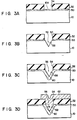
- the substrate 10 above which the insulative layer 52 is formed is subjected to a well-known photolithography and, as shown in Fig. 3A, an opening 54 is formed in the portion of the insulative layer 52 corresponding to the contact region of the substrate 10.
- anisotropic etching is performed to form a concave portion 56 having a V-shaped cross section in a partial surface 10a of the substrate 10 which is exposed through the opening 54.
- anisotropic etching technique it is desirable to use reactive ion etching (RIE) using etching gases such as C x Hy, CI 2 and the like. It is also possible to use a conventional wet etching technique using an etching fluid such as KOH. Photo-excited dry etching process is also applicable.
- the concave portion 56 formed by this etching has slanted surfaces 58 which are inclined by only a predetermined angle with respect to the substrate surface similar to the device of Fig. 1.
- the concave portion 56 is deeply formed so as to pierce the n-type semiconductive layer 50 formed in the surface portion of the substrate 10 as shown in Fig. 3B.
- the etching technology itself to form the recessed portion with the desired cross section of in the substrate 10 is well known. For instance, it is disclosed in:
- arsenic ions are implanted as n-type impurities into the substrate region in which the concave portion 56 having the V-shaped cross section under the condition of, for example, 50 kV and 1 x 10 15 /c m -2 . Since the recessed contact region 58 has the V-shaped cross section, the ions can be relatively easily implanted into the recessed portion of the substrate 10.
- the substrate 10 into which ions were implanted is heated to a proper temperature and the implanted ions are thermally diffused, so that an n-type diffusion layer 60 is formed surrounding the V-shaped contact concave portion 56.
- the n-type diffusion layer 60 again connects the n-type layer 50 which was partially cut due to the formation of the V-shaped contact concave portion 56. It should be noted that the thicknesses of the n-type layers 50 and 60 (namely, the depths of the diffusion layers) differ from each other since the steps of forming the n-type layers 50 and 60 differ. The thickness of the V-shaped diffusion layer 60 may be substantially equal to, larger or smaller than the thickness of the previous diffusion layer 50. "
- a metal wiring layer 62 made of, for instance, aluminum silicon alloy is deposited on the insulative layer 52 and is sintered for a suitable period of time (for example, thirty minutes) in atmosphere of forming gas (for instance, a mixture of nitrogen and hydrogen) at a suitable temperature (e.g., 450°C).
- atmosphere of forming gas for instance, a mixture of nitrogen and hydrogen
- a suitable temperature e.g., 450°C
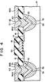
- Fig. 4 shows an embodiment of the invention, this being a modified form of the semiconductor integrated circuit device having the V-shaped contact concave portion shown in Fig. 1.
- similar portions as those in Fig. 1 are designated by the same reference numerals and detailed descriptions thereof are omitted.
- the source and drain regions 12 and 14 of the MOS FET 0 1 extend into two contact regions C 1 and C z .
- An opening 70 is formed in the insulative layer 18 and defines the second contact regions C 2 .
- a concave portion 72 having a V-shaped cross section is formed in the second contact region C 2 of the substrate 10.
- Another n-type diffusion layer 74 is formed so as to surround the V-shaped contact concave portion 72.
- the n-type diffusion layer 74 is continuously connected with the source region 12 of the FET 0 1 and has a thickness larger than the depth of the source region 12.
- Impurities having the same conductivity type as that of the substrate 10; namely, having the p-type are implanted into the contact regions C 1 and C 2 of the substrate 10 so as to provide p-type semiconductor layers 76 and 78 which surround the V-shaped thick n-type diffusion layers 24 and 74.
- boron ions are selected as the p-type impurities.
- V-shaped contact concave portions 22 and 72 surrounded by the p-type semiconductor layers (referred to as "p well regions" in this specification) 76 and 78 are formed on both sides of the source and drain regions 12 and 14 of one MOS FET Q i , it is possible to prevent the occurrence of "punch through” which result in a leakage current flowing between the V-shaped contact concave portions 22 and 72. This is because a current loss from the n-type diffusion layers 24 and 74 to the substrate 10 can be reliably prevented since the concentration of p-type impurities is set to be high in the substrate portion which is in contact with the neighboring V-shaped n-type diffusion layers 24 and 74.
- the metal wiring layer has a double-layered structure.
- a first metal layer (such as tungsten) 80a is buried in the contact hole 22 formed in the insulative layer 18.
- the contact region can be easily refilled with tungsten by using a CVD method wherein WF 6 gas is reduced by H 2 gas or silicon.
- the surface of the metal layer 80a is recessed and has an increased surface area.
- a second metal layer 80b is stacked on the insulative layer 18 so as to be electrically connected with the first metal layer 80a through the recessed surface portion 82. Consequently, a metal wiring layer 80 for the contact region C, is formed.
- a metal wiring layer 84 for the other contact region C 2 is also constructed of upper and lower metal layers 84b and 84a which are mutually stacked in the contact region C 2 in a similar manner as the case of the contact region C i .
- the manufacturing of the wiring of the highly integrated semiconductor device can be simplified by adopting of such a double-layered metal wiring structure. Further, although this structure is double-layered, the upper and lower metal layers 80b and 80a (84b and 84a) are electrically in contact with each other through the increased surface portion 82 and, consequently, the contact resistance between the metals can be reduced compared with a simple flat interface.
- the cross sectional shape of concave portion in the recessed contact region in the devices shown in Fig. 1 and Fig. 4 is not limited to the above-mentioned V-shaped cross section but may be variably modified as illustrated in Figs. 5 to 8, respectively.
- the similar portions as those shown in the foregoing are designated by the same reference numerals.
- a contact concave portion 100 formed in the p-type substrate 10 has a rectangular cross section having no slanted surface.
- an n-type semiconductive layer 102 into which n-type impurities were implanted is formed along the configuration of the substrate surface in the contact region of the substrate 10 so as to surround the contact concave portion 100 having a rectangular cross section.
- the n-type impurity layer 102 can be formed in the following manner.
- n-type impurities are- implanted into the bottom portion of the rectangular contact concave portion 100 and then this substrate is subjected to thermal diffusion treatment, so that the n-type impurity layer portion extending along the vertical wall of the rectangular contact concave portion 100 can be formed.
- a contact concave portion 104 formed in the substrate 10 has slanted surfaces 106 at the bottom portion.
- a contact concave portion 108 has slanted surfaces that reach the substrate surface and also has a horizontal surface at the bottom portion.
- a contact concave portion 110 has vertical side walls that reach the substrate surface and also has V-shaped slanted surfaces at the bottom portion.
Landscapes
- Internal Circuitry In Semiconductor Integrated Circuit Devices (AREA)
- Electrodes Of Semiconductors (AREA)
Claims (10)
Applications Claiming Priority (2)
| Application Number | Priority Date | Filing Date | Title |
|---|---|---|---|
| JP182810/84 | 1984-09-03 | ||
| JP59182810A JPS6161441A (ja) | 1984-09-03 | 1984-09-03 | 半導体装置の製造方法 |
Publications (3)
| Publication Number | Publication Date |
|---|---|
| EP0174185A2 EP0174185A2 (de) | 1986-03-12 |
| EP0174185A3 EP0174185A3 (en) | 1988-01-07 |
| EP0174185B1 true EP0174185B1 (de) | 1990-01-03 |
Family
ID=16124832
Family Applications (1)
| Application Number | Title | Priority Date | Filing Date |
|---|---|---|---|
| EP85306249A Expired - Lifetime EP0174185B1 (de) | 1984-09-03 | 1985-09-03 | Halbleiteranordnung und Verfahren zum Herstellen derselben |
Country Status (5)
| Country | Link |
|---|---|
| US (2) | US4860084A (de) |
| EP (1) | EP0174185B1 (de) |
| JP (1) | JPS6161441A (de) |
| KR (1) | KR900008359B1 (de) |
| DE (1) | DE3575241D1 (de) |
Families Citing this family (37)
| Publication number | Priority date | Publication date | Assignee | Title |
|---|---|---|---|---|
| JPH04368182A (ja) * | 1991-06-17 | 1992-12-21 | Mitsubishi Electric Corp | 半導体装置およびその製造方法 |
| US4795436A (en) * | 1983-11-14 | 1989-01-03 | Bio-Mimetics, Inc. | Bioadhesive composition and method of treatment therewith |
| JPH0226049A (ja) * | 1988-07-14 | 1990-01-29 | Matsushita Electron Corp | 半導体装置の製造方法 |
| US5084418A (en) * | 1988-12-27 | 1992-01-28 | Texas Instruments Incorporated | Method of making an array device with buried interconnects |
| US5216264A (en) * | 1989-06-07 | 1993-06-01 | Sharp Kabushiki Kaisha | Silicon carbide MOS type field-effect transistor with at least one of the source and drain regions is formed by the use of a schottky contact |
| US5585288A (en) * | 1990-07-16 | 1996-12-17 | Raytheon Company | Digital MMIC/analog MMIC structures and process |
| JPH0496336A (ja) * | 1990-08-11 | 1992-03-27 | Nec Corp | Mos型半導体装置 |
| US5506421A (en) * | 1992-11-24 | 1996-04-09 | Cree Research, Inc. | Power MOSFET in silicon carbide |
| US5447871A (en) * | 1993-03-05 | 1995-09-05 | Goldstein; Edward F. | Electrically conductive interconnection through a body of semiconductor material |
| US6310384B1 (en) * | 1993-07-02 | 2001-10-30 | Hitachi, Ltd. | Low stress semiconductor devices with thermal oxide isolation |
| US5466616A (en) * | 1994-04-06 | 1995-11-14 | United Microelectronics Corp. | Method of producing an LDMOS transistor having reduced dimensions, reduced leakage, and a reduced propensity to latch-up |
| US5395777A (en) * | 1994-04-06 | 1995-03-07 | United Microelectronics Corp. | Method of producing VDMOS transistors |
| US5387534A (en) * | 1994-05-05 | 1995-02-07 | Micron Semiconductor, Inc. | Method of forming an array of non-volatile sonos memory cells and array of non-violatile sonos memory cells |
| FR2720191B1 (fr) * | 1994-05-18 | 1996-10-18 | Michel Haond | Transistor à effet de champ à grille isolée, et procédé de fabrication correspondant. |
| US5895766A (en) * | 1995-09-20 | 1999-04-20 | Micron Technology, Inc. | Method of forming a field effect transistor |
| JP3012187B2 (ja) * | 1996-02-05 | 2000-02-21 | 松下電子工業株式会社 | 半導体装置の製造方法 |
| US5831312A (en) * | 1996-04-09 | 1998-11-03 | United Microelectronics Corporation | Electrostic discharge protection device comprising a plurality of trenches |
| US5721146A (en) * | 1996-04-29 | 1998-02-24 | Taiwan Semiconductor Manufacturing Company Ltd | Method of forming buried contact architecture within a trench |
| US5719409A (en) * | 1996-06-06 | 1998-02-17 | Cree Research, Inc. | Silicon carbide metal-insulator semiconductor field effect transistor |
| US5736418A (en) * | 1996-06-07 | 1998-04-07 | Lsi Logic Corporation | Method for fabricating a field effect transistor using microtrenches to control hot electron effects |
| TW313674B (en) * | 1996-09-21 | 1997-08-21 | United Microelectronics Corp | High pressure metal oxide semiconductor device and manufacturing method thereof |
| DE19711165A1 (de) * | 1997-03-18 | 1998-09-24 | Smi Syst Microelect Innovat | Kontaktanordnung einer planaren, integrierbaren Halbleiteranordnung und Verfahren zur Herstellung dieser Kontaktanordnung |
| US6297533B1 (en) * | 1997-12-04 | 2001-10-02 | The Whitaker Corporation | LDMOS structure with via grounded source |
| US6153934A (en) * | 1998-07-30 | 2000-11-28 | International Business Machines Corporation | Buried butted contact and method for fabricating |
| JP3996286B2 (ja) * | 1998-11-27 | 2007-10-24 | 株式会社ルネサステクノロジ | 半導体装置およびその製造方法 |
| JP3566885B2 (ja) * | 1999-06-02 | 2004-09-15 | シャープ株式会社 | トレンチアイソレーションの形成方法及び半導体装置の製造方法 |
| US7217977B2 (en) * | 2004-04-19 | 2007-05-15 | Hrl Laboratories, Llc | Covert transformation of transistor properties as a circuit protection method |
| US6815816B1 (en) * | 2000-10-25 | 2004-11-09 | Hrl Laboratories, Llc | Implanted hidden interconnections in a semiconductor device for preventing reverse engineering |
| US7049667B2 (en) | 2002-09-27 | 2006-05-23 | Hrl Laboratories, Llc | Conductive channel pseudo block process and circuit to inhibit reverse engineering |
| WO2004055868A2 (en) | 2002-12-13 | 2004-07-01 | Hrl Laboratories, Llc | Integrated circuit modification using well implants |
| JP2004363302A (ja) * | 2003-06-04 | 2004-12-24 | Toshiba Corp | Mosfet |
| KR100604527B1 (ko) * | 2003-12-31 | 2006-07-24 | 동부일렉트로닉스 주식회사 | 바이폴라 트랜지스터 제조방법 |
| US7242063B1 (en) | 2004-06-29 | 2007-07-10 | Hrl Laboratories, Llc | Symmetric non-intrusive and covert technique to render a transistor permanently non-operable |
| KR101101192B1 (ko) * | 2004-08-26 | 2012-01-03 | 동부일렉트로닉스 주식회사 | 반도체 소자의 금속 배선 형성 방법 |
| US8168487B2 (en) | 2006-09-28 | 2012-05-01 | Hrl Laboratories, Llc | Programmable connection and isolation of active regions in an integrated circuit using ambiguous features to confuse a reverse engineer |
| CN113611736B (zh) * | 2020-05-29 | 2022-11-22 | 联芯集成电路制造(厦门)有限公司 | 半导体元件及其制作方法 |
| US12610605B2 (en) * | 2022-11-28 | 2026-04-21 | Globalfoundries U.S. Inc. | IC structure with gate electrode fully within V-shaped cavity |
Family Cites Families (20)
| Publication number | Priority date | Publication date | Assignee | Title |
|---|---|---|---|---|
| US3553536A (en) * | 1968-11-19 | 1971-01-05 | Rca Corp | Semiconductor rectifiers having controlled storage and recovery characteristics |
| GB1507061A (en) * | 1974-03-26 | 1978-04-12 | Signetics Corp | Semiconductors |
| US4151546A (en) * | 1976-01-14 | 1979-04-24 | Tokyo Shibaura Electric Co., Ltd. | Semiconductor device having electrode-lead layer units of differing thicknesses |
| JPS5363983A (en) * | 1976-11-19 | 1978-06-07 | Toshiba Corp | Semiconductor device |
| JPS5379378A (en) * | 1976-12-23 | 1978-07-13 | Matsushita Electric Ind Co Ltd | Semoconductor davice and its production |
| US4116720A (en) * | 1977-12-27 | 1978-09-26 | Burroughs Corporation | Method of making a V-MOS field effect transistor for a dynamic memory cell having improved capacitance |
| JPS55107260A (en) * | 1979-02-08 | 1980-08-16 | Shindengen Electric Mfg Co Ltd | Power transistor |
| DE2929939A1 (de) * | 1979-07-24 | 1981-02-19 | Licentia Gmbh | Halbleiteranordnung und verfahren zu ihrer herstellung |
| JPS5633823A (en) * | 1979-08-29 | 1981-04-04 | Toshiba Corp | Preparation of semiconductor device |
| JPS56111217A (en) * | 1980-02-07 | 1981-09-02 | Chiyou Lsi Gijutsu Kenkyu Kumiai | Preparation of semiconductor device |
| US4397075A (en) * | 1980-07-03 | 1983-08-09 | International Business Machines Corporation | FET Memory cell structure and process |
| EP0067566A3 (de) * | 1981-06-13 | 1985-08-07 | Plessey Overseas Limited | Integrierter Lichtdetektor oder -generator mit Verstärker |
| US4458259A (en) * | 1981-11-12 | 1984-07-03 | Gte Laboratories Incorporated | Etched-source static induction transistor |
| JPS58137245A (ja) * | 1982-02-10 | 1983-08-15 | Hitachi Ltd | 大規模半導体メモリ |
| US4625388A (en) * | 1982-04-26 | 1986-12-02 | Acrian, Inc. | Method of fabricating mesa MOSFET using overhang mask and resulting structure |
| US4503598A (en) * | 1982-05-20 | 1985-03-12 | Fairchild Camera & Instrument Corporation | Method of fabricating power MOSFET structure utilizing self-aligned diffusion and etching techniques |
| JPS5963719A (ja) * | 1982-10-04 | 1984-04-11 | Matsushita Electronics Corp | 半導体装置 |
| JPS60126861A (ja) * | 1983-12-13 | 1985-07-06 | Fujitsu Ltd | 半導体記憶装置 |
| US4622569A (en) * | 1984-06-08 | 1986-11-11 | Eaton Corporation | Lateral bidirectional power FET with notched multi-channel stacking and with dual gate reference terminal means |
| US4633281A (en) * | 1984-06-08 | 1986-12-30 | Eaton Corporation | Dual stack power JFET with buried field shaping depletion regions |
-
1984
- 1984-09-03 JP JP59182810A patent/JPS6161441A/ja active Pending
-
1985
- 1985-06-05 KR KR1019850003944A patent/KR900008359B1/ko not_active Expired
- 1985-09-03 DE DE8585306249T patent/DE3575241D1/de not_active Expired - Lifetime
- 1985-09-03 EP EP85306249A patent/EP0174185B1/de not_active Expired - Lifetime
-
1989
- 1989-01-03 US US07/293,570 patent/US4860084A/en not_active Expired - Fee Related
- 1989-06-07 US US07/362,653 patent/US4914050A/en not_active Expired - Fee Related
Also Published As
| Publication number | Publication date |
|---|---|
| JPS6161441A (ja) | 1986-03-29 |
| EP0174185A2 (de) | 1986-03-12 |
| KR860002862A (ko) | 1986-04-30 |
| KR900008359B1 (ko) | 1990-11-17 |
| US4860084A (en) | 1989-08-22 |
| DE3575241D1 (de) | 1990-02-08 |
| US4914050A (en) | 1990-04-03 |
| EP0174185A3 (en) | 1988-01-07 |
Similar Documents
| Publication | Publication Date | Title |
|---|---|---|
| EP0174185B1 (de) | Halbleiteranordnung und Verfahren zum Herstellen derselben | |
| US4683643A (en) | Method of manufacturing a vertical MOSFET with single surface electrodes | |
| US6518128B2 (en) | Trench MOSFET with double-diffused body profile | |
| US6114207A (en) | Method of producing a semiconductor device | |
| KR100976526B1 (ko) | 반도체 디바이스 및 반도체 디바이스 제조 방법 | |
| US5442214A (en) | VDMOS transistor and manufacturing method therefor | |
| JP3387563B2 (ja) | 電界効果トランジスタ及びその製造方法 | |
| US7049194B2 (en) | Trench DMOS device with improved drain contact | |
| US6872611B2 (en) | Method of manufacturing transistor | |
| US6627951B2 (en) | High speed trench DMOS | |
| EP0345380B1 (de) | Verfahren zur Herstellung eines Halbleiterbauelements | |
| US6867456B2 (en) | Semiconductor device having high breakdown voltage without increased on resistance | |
| US6774408B2 (en) | Trench gate power device having a concentration at channel layer higher than a base layer and uniformly distributed along the depth of the trench and its manufacturing method | |
| US4786953A (en) | Vertical MOSFET and method of manufacturing the same | |
| EP1052690A2 (de) | Verfahren zur Herstellung von Bauelementen mit MOS-Gate und selbstjustierten Gräben | |
| JP2000164869A (ja) | ブレ―クダウン特性及びオン抵抗特性を改善したトレンチ形mosfet並びにその製造方法 | |
| US4486266A (en) | Integrated circuit method | |
| KR100883795B1 (ko) | 대칭적인 트렌치 mosfet 디바이스 및 그 제조 방법 | |
| US4454523A (en) | High voltage field effect transistor | |
| EP0090520B1 (de) | Verfahren zur Herstellung einer Halbleiteranordnung mit einer tiefen Isolationszone in einem Halbleiter | |
| US4975754A (en) | Trench dual-gate MOSFET | |
| US8133788B2 (en) | Method of manufacturing semiconductor device | |
| KR0173458B1 (ko) | 반도체집적회로 및 그 제조방법 | |
| US5254867A (en) | Semiconductor devices having an improved gate | |
| US7176533B2 (en) | Semiconductor devices having contact plugs including polysilicon doped with an impurity having a lesser diffusion coefficient than phosphorus |
Legal Events
| Date | Code | Title | Description |
|---|---|---|---|
| PUAI | Public reference made under article 153(3) epc to a published international application that has entered the european phase |
Free format text: ORIGINAL CODE: 0009012 |
|
| 17P | Request for examination filed |
Effective date: 19850916 |
|
| AK | Designated contracting states |
Kind code of ref document: A2 Designated state(s): DE FR GB |
|
| PUAL | Search report despatched |
Free format text: ORIGINAL CODE: 0009013 |
|
| AK | Designated contracting states |
Kind code of ref document: A3 Designated state(s): DE FR GB |
|
| 17Q | First examination report despatched |
Effective date: 19880419 |
|
| GRAA | (expected) grant |
Free format text: ORIGINAL CODE: 0009210 |
|
| AK | Designated contracting states |
Kind code of ref document: B1 Designated state(s): DE FR GB |
|
| PG25 | Lapsed in a contracting state [announced via postgrant information from national office to epo] |
Ref country code: FR Free format text: THE PATENT HAS BEEN ANNULLED BY A DECISION OF A NATIONAL AUTHORITY Effective date: 19900103 |
|
| REF | Corresponds to: |
Ref document number: 3575241 Country of ref document: DE Date of ref document: 19900208 |
|
| EN | Fr: translation not filed | ||
| PG25 | Lapsed in a contracting state [announced via postgrant information from national office to epo] |
Ref country code: GB Effective date: 19900903 |
|
| PLBE | No opposition filed within time limit |
Free format text: ORIGINAL CODE: 0009261 |
|
| STAA | Information on the status of an ep patent application or granted ep patent |
Free format text: STATUS: NO OPPOSITION FILED WITHIN TIME LIMIT |
|
| 26N | No opposition filed | ||
| GBPC | Gb: european patent ceased through non-payment of renewal fee | ||
| PGFP | Annual fee paid to national office [announced via postgrant information from national office to epo] |
Ref country code: DE Payment date: 20040902 Year of fee payment: 20 |