EP0175461B1 - Corps de bobine - Google Patents
Corps de bobine Download PDFInfo
- Publication number
- EP0175461B1 EP0175461B1 EP85305308A EP85305308A EP0175461B1 EP 0175461 B1 EP0175461 B1 EP 0175461B1 EP 85305308 A EP85305308 A EP 85305308A EP 85305308 A EP85305308 A EP 85305308A EP 0175461 B1 EP0175461 B1 EP 0175461B1
- Authority
- EP
- European Patent Office
- Prior art keywords
- core
- contact element
- coil assembly
- winding
- electrically connected
- Prior art date
- Legal status (The legal status is an assumption and is not a legal conclusion. Google has not performed a legal analysis and makes no representation as to the accuracy of the status listed.)
- Expired
Links
Images
Classifications
-
- H—ELECTRICITY
- H01—ELECTRIC ELEMENTS
- H01F—MAGNETS; INDUCTANCES; TRANSFORMERS; SELECTION OF MATERIALS FOR THEIR MAGNETIC PROPERTIES
- H01F27/00—Details of transformers or inductances, in general
-
- H—ELECTRICITY
- H01—ELECTRIC ELEMENTS
- H01F—MAGNETS; INDUCTANCES; TRANSFORMERS; SELECTION OF MATERIALS FOR THEIR MAGNETIC PROPERTIES
- H01F27/00—Details of transformers or inductances, in general
- H01F27/28—Coils; Windings; Conductive connections
- H01F27/29—Terminals; Tapping arrangements for signal inductances
-
- H—ELECTRICITY
- H01—ELECTRIC ELEMENTS
- H01F—MAGNETS; INDUCTANCES; TRANSFORMERS; SELECTION OF MATERIALS FOR THEIR MAGNETIC PROPERTIES
- H01F5/00—Coils
- H01F5/04—Arrangements of electric connections to coils, e.g. leads
-
- H—ELECTRICITY
- H01—ELECTRIC ELEMENTS
- H01F—MAGNETS; INDUCTANCES; TRANSFORMERS; SELECTION OF MATERIALS FOR THEIR MAGNETIC PROPERTIES
- H01F5/00—Coils
- H01F5/04—Arrangements of electric connections to coils, e.g. leads
- H01F2005/046—Details of formers and pin terminals related to mounting on printed circuits
-
- H—ELECTRICITY
- H05—ELECTRIC TECHNIQUES NOT OTHERWISE PROVIDED FOR
- H05K—PRINTED CIRCUITS; CASINGS OR CONSTRUCTIONAL DETAILS OF ELECTRIC APPARATUS; MANUFACTURE OF ASSEMBLAGES OF ELECTRICAL COMPONENTS
- H05K3/00—Apparatus or processes for manufacturing printed circuits
- H05K3/30—Assembling printed circuits with electric components, e.g. with resistors
- H05K3/306—Assembling printed circuits with electric components, e.g. with resistors with lead-in-hole components
- H05K3/308—Adaptations of leads
Definitions
- This invention relates generally to inductors and more particularly concerns a coil assembly including a core, a winding on the core, and a contact element electrically connected to the winding which is both mechanically clamped and bonded to the core.
- One type of conventional coil assembly takes the form of a core, often of a magnetic material such as a ferrite, and a winding wound on the core. Means are provided for making electrical connections to the winding to permit the use of the coil in an electrical circuit. Means are also provided for physically mounting the coil assembly in a circuit, such as on a printed circuit board. Such coils may be surface mounted on a printed circuit board, wherein the coils are soldered to the copper pattern side of the board; or, the coil mounting assembly may include pins which pass through the board, and which are soldered to the underside of the board.
- an electrically conductive contact element, or pad is bonded to a portion of the core and subsequently soldered onto the printed circuit board.
- two such contact elements spaced apart from one another on the core, are provided; and one end of the winding is soldered to one of the contact elements, and the other end of the winding is soldered to the other contact element.
- the contact elements, and connected winding terminations, are then soldered onto the printed circuit board.
- a iayer of epoxy is applied to the contact element or to a location on the core to which the contact element, or pad, is to be bonded, and the pad is held in place on the core until the epoxy has cured to establish the desired bond.
- such pads might have edge dimensions of a few millimeters or less. The manipulation and alignment of the pads, and the maintenance of the pads in position during bonding can be extremely difficult.
- a coil assembly in accordance with the invention comprises, a core, an inductive winding on the core and an electrically conductive contact element on the core characterised in that the contact element is formed to have a web and at least two generally opposed portions which apply a clamping force to the core the element being electrically connected to a first location on the winding and in that adhesive means for bonding the contact element to the core are applied between the web and the core, the clamping element serving to hold the contact element in place on the core during bonding.
- a generally U-shaped contact element is clamped onto each foot of a C-core and also bonded to the bottom of the core foot.
- Each end of a winding on the core is soldered to a different one of the contact elements, and the completed coil assembly may be subsequently connected into an electrical circuit such as by soldering onto a printed circuit board.
- the mechanical clamping force of each contact element holds the element in place on the C-core foot during bonding so that each contact element need not be held in place during bonding.
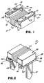
- a microcoil assembly 11 includes a core 12 upon which is wound a winding 13.
- the core 12 is a C-core having a winding-bearing portion and two feet 14, 16.
- One end of the winding 13 is electrically connected to a contact element 17 on the foot 14, and the other end of the winding 13 is electrically connected to a contact element 18 on the foot 16.
- the contact element 17 is generally U-shaped, having a pair of legs 19, 21 joined by an intermediate web portion 22.
- a layer of epoxy 23 is applied to the bottom surface of the foot 14, or to the mating surface of the contact element, and the contact element is mechanically secured on the core foot with the epoxy layer pressed between the web portion 22 of the contact element and the bottom of the foot of the core.
- the web 22 of the contact element is bent slightly, spreading the legs 19, 21 slightly apart, and the contact element is positioned with the legs 19, 21 on opposite sides of the core foot 14.
- the legs 19, 21 move toward one another and grip the foot 14 of the core 12, applying a mechanical clamping force to the core and holding the contact element in position. After the epoxy 23 has cured, the contact element is bonded to the core and held securely in position.
- the contact element 18 has a pair of legs 24, 26 joined by an intermediate web portion 27 and is mounted on the core leg 16 in the same fashion as the contact element 17 is mechanically secured on the foot 14 of the core 12.
- the end of the winding is soldered to the lower surface of the web 22 of the contact element 17.
- the second end of the winding 13 is soldered to the lower surface of the intermediate web 27 of the contact element 18.
- the coil assembly 11 may then be surface mounted on a printed circuit board by soldering the bottom surfaces of the webs 22, 27 to the appropriate portions of the copper pattern on the printed circuit board.
- a visible solder joint is produced so that proper electrical connection of the assembly to the board can be visually verified. This visible solder joint is produced along the outer faces of the legs such as 19 adjacent the circuit board.
- a coil assembly 31 includes a winding 33 wound on a core 32 which includes a pair of feet 34, 36.
- the ends of the winding 33 are soldered to a pair of contact elements 37, 38 which are secured to the core feet 34, 36 respectively.
- the contact element 37 has a pair of legs 39, 41 joined by an intermediate web portion 42.
- the contact element 37 is clamped and bonded to the core foot 34 in the same manner as the contact element 17 is secured to the foot 14 in the coil assembly 11.
- the contact element 38 is substantially identical to the contact element 37 and is attached to the core foot 36 in the same manner as the contact element 37 is secured to the core foot 34.
- The- contact element 37 further includes a downwardly extending pin portion 51.
- the element 38 also includes a downwardly extending pin portion 52.
- the coil assembly 31 may be mounted on a printed circuit board by inserting the pins 51, 52 through holes in the printed circuit board and soldering the pins to the appropriate portions of the copper pattern on the underside of the board. Electrical connection from the circuit board to the winding 33 is provided via the contact elements 37, 38 to which the ends of the coil 33 are soldered.
- the invention has now been described in connection with coil assemblies employing C-cores, many other types of core configurations may be employed in practicing the invention.
- the contact elements may be mounted on an I-core (having no feet), with the contact elements serving to maintain the coil winding spaced apart from the board.
Landscapes
- Engineering & Computer Science (AREA)
- Power Engineering (AREA)
- Coils Or Transformers For Communication (AREA)
- Magnetic Resonance Imaging Apparatus (AREA)
- Ignition Installations For Internal Combustion Engines (AREA)
Claims (12)
Applications Claiming Priority (2)
| Application Number | Priority Date | Filing Date | Title |
|---|---|---|---|
| US06/640,945 US4588974A (en) | 1984-08-15 | 1984-08-15 | Coil assembly having clamped and bonded contacts |
| US640945 | 1984-08-15 |
Publications (2)
| Publication Number | Publication Date |
|---|---|
| EP0175461A1 EP0175461A1 (fr) | 1986-03-26 |
| EP0175461B1 true EP0175461B1 (fr) | 1989-03-08 |
Family
ID=24570318
Family Applications (1)
| Application Number | Title | Priority Date | Filing Date |
|---|---|---|---|
| EP85305308A Expired EP0175461B1 (fr) | 1984-08-15 | 1985-07-25 | Corps de bobine |
Country Status (5)
| Country | Link |
|---|---|
| US (1) | US4588974A (fr) |
| EP (1) | EP0175461B1 (fr) |
| JP (1) | JPS6159707A (fr) |
| KR (1) | KR860002118A (fr) |
| DE (1) | DE3568665D1 (fr) |
Families Citing this family (11)
| Publication number | Priority date | Publication date | Assignee | Title |
|---|---|---|---|---|
| DE3615307C2 (de) * | 1986-05-06 | 1994-07-07 | Johann Leonhard Huettlinger | Spule für automatische SMD-Bestückung |
| DE3708742A1 (de) * | 1987-03-18 | 1988-10-06 | Bosch Gmbh Robert | Ferritkernspuele mit mehr als zwei spulenanschluessen fuer reflow-loetung auf einer leiterplatte |
| US4725806A (en) * | 1987-05-21 | 1988-02-16 | Standex International Corporation | Contact elements for miniature inductor |
| DE4217434A1 (de) * | 1992-05-26 | 1993-12-02 | Siemens Ag | Elektrisches Bauteil |
| GB2298316B (en) * | 1995-02-23 | 1998-12-16 | Standex Int Corp | Surface mount electronic reed switch component |
| GB2342509A (en) * | 1998-10-05 | 2000-04-12 | Standex Int Corp | Surface mount reed switch having transverse feet formed from leads |
| IL161373A (en) * | 2004-04-14 | 2008-11-03 | Iscar Ltd | Cutting tool and cutting insert therefor |
| TW200743434A (en) * | 2006-05-11 | 2007-11-16 | Delta Electronics Inc | Packaged electronic component for shielding electromagnetic interference |
| IL178377A (en) * | 2006-09-28 | 2010-06-30 | Iscar Ltd | Cutting tool and cutting tool fastened by its external clamp |
| RU2539537C1 (ru) * | 2013-08-05 | 2015-01-20 | Нина Алексеевна Корюкина | Режущая пластина, сборная режущая пластина и сборный режущий инструмент |
| CN110391074B (zh) * | 2019-07-01 | 2020-10-13 | 广州市一变电气设备有限公司 | 低噪音节能环保变压器 |
Family Cites Families (8)
| Publication number | Priority date | Publication date | Assignee | Title |
|---|---|---|---|---|
| GB815595A (en) * | 1955-11-02 | 1959-07-01 | Cole E K Ltd | Improvements in or relating to inductance coils |
| US3697817A (en) * | 1971-01-25 | 1972-10-10 | Rca Corp | Mounting attachment for a modular substrate |
| JPS585317B2 (ja) * | 1974-12-12 | 1983-01-29 | 日本化薬株式会社 | セルロ−ズケイセンイノ センシヨクホウ |
| US4004200A (en) * | 1975-07-21 | 1977-01-18 | Johanson Manufacturing Corporation | Chip capacitor with spring-like leads |
| DE2617465C3 (de) * | 1976-04-21 | 1978-10-19 | Siemens Ag, 1000 Berlin Und 8000 Muenchen | Elektrische Spule und Verfahren zu ihrer Herstellung |
| US4245207A (en) * | 1977-05-20 | 1981-01-13 | Toko, Inc. | Miniature high frequency coil assembly or transformer |
| FR2506504B1 (fr) * | 1981-05-19 | 1985-10-11 | Europ Composants Electron | Circuit magnetique, inductance utilisant un tel circuit et procede de realisation dudit circuit magnetique |
| JPS58166713A (ja) * | 1982-03-29 | 1983-10-01 | Toko Inc | 固定インダクタの製造方法 |
-
1984
- 1984-08-15 US US06/640,945 patent/US4588974A/en not_active Expired - Fee Related
-
1985
- 1985-07-25 DE DE8585305308T patent/DE3568665D1/de not_active Expired
- 1985-07-25 EP EP85305308A patent/EP0175461B1/fr not_active Expired
- 1985-08-14 KR KR1019850005849A patent/KR860002118A/ko not_active Ceased
- 1985-08-14 JP JP60177807A patent/JPS6159707A/ja active Pending
Also Published As
| Publication number | Publication date |
|---|---|
| US4588974A (en) | 1986-05-13 |
| KR860002118A (ko) | 1986-03-26 |
| DE3568665D1 (en) | 1989-04-13 |
| JPS6159707A (ja) | 1986-03-27 |
| EP0175461A1 (fr) | 1986-03-26 |
Similar Documents
| Publication | Publication Date | Title |
|---|---|---|
| US5055971A (en) | Magnetic component using core clip arrangement operative for facilitating pick and place surface mount | |
| EP0387441B1 (fr) | Montage en surface d'un élément inductif | |
| US4588974A (en) | Coil assembly having clamped and bonded contacts | |
| JP3173654B2 (ja) | インダクタンス素子 | |
| EP0291602B1 (fr) | Eléments de contact pour inductance miniature | |
| EP1168385B1 (fr) | Appareil à bobine et son procédé de fabrication | |
| US6727794B2 (en) | Apparatus for establishing inductive coupling in an electrical circuit and method of manufacture therefor | |
| JPH0543453Y2 (fr) | ||
| US20040058593A1 (en) | Coupling adjusting structure for double-tuned circuit | |
| JP3426564B2 (ja) | 表面実装チョークコイル | |
| JPS62278776A (ja) | 電気的又は電子的な素子のためのはんだ付け接続装置 | |
| JP3614490B2 (ja) | コイル装置 | |
| JPH04142716A (ja) | 電磁機器の回路基板への取付け方法 | |
| JPH06151178A (ja) | コイル | |
| JPH02148705A (ja) | インダクタンス素子 | |
| JPS6223054Y2 (fr) | ||
| JPH0817653A (ja) | 積層型コイル及びその製造方法 | |
| JPH04105512U (ja) | 積層シートコイル装置 | |
| JPH07297048A (ja) | コイルコア部材を有する回路基板 | |
| JP2594365B2 (ja) | 配線基板及び配線基板の接続方法 | |
| JP3571094B2 (ja) | 薄型トランス | |
| JPH03133109A (ja) | プリント基板実装形コイル | |
| JPH0353455Y2 (fr) | ||
| JPH0737731A (ja) | トランス装置及びその製造方法 | |
| JPH0115121Y2 (fr) |
Legal Events
| Date | Code | Title | Description |
|---|---|---|---|
| PUAI | Public reference made under article 153(3) epc to a published international application that has entered the european phase |
Free format text: ORIGINAL CODE: 0009012 |
|
| AK | Designated contracting states |
Kind code of ref document: A1 Designated state(s): DE FR GB NL |
|
| 17P | Request for examination filed |
Effective date: 19860718 |
|
| 17Q | First examination report despatched |
Effective date: 19871112 |
|
| GRAA | (expected) grant |
Free format text: ORIGINAL CODE: 0009210 |
|
| AK | Designated contracting states |
Kind code of ref document: B1 Designated state(s): DE FR GB NL |
|
| REF | Corresponds to: |
Ref document number: 3568665 Country of ref document: DE Date of ref document: 19890413 |
|
| ET | Fr: translation filed | ||
| PLBE | No opposition filed within time limit |
Free format text: ORIGINAL CODE: 0009261 |
|
| STAA | Information on the status of an ep patent application or granted ep patent |
Free format text: STATUS: NO OPPOSITION FILED WITHIN TIME LIMIT |
|
| 26N | No opposition filed | ||
| PGFP | Annual fee paid to national office [announced via postgrant information from national office to epo] |
Ref country code: FR Payment date: 19940711 Year of fee payment: 10 |
|
| PGFP | Annual fee paid to national office [announced via postgrant information from national office to epo] |
Ref country code: GB Payment date: 19940718 Year of fee payment: 10 |
|
| PGFP | Annual fee paid to national office [announced via postgrant information from national office to epo] |
Ref country code: DE Payment date: 19940721 Year of fee payment: 10 |
|
| PGFP | Annual fee paid to national office [announced via postgrant information from national office to epo] |
Ref country code: NL Payment date: 19940731 Year of fee payment: 10 |
|
| PG25 | Lapsed in a contracting state [announced via postgrant information from national office to epo] |
Ref country code: GB Effective date: 19950725 |
|
| PG25 | Lapsed in a contracting state [announced via postgrant information from national office to epo] |
Ref country code: NL Effective date: 19960201 |
|
| GBPC | Gb: european patent ceased through non-payment of renewal fee |
Effective date: 19950725 |
|
| NLV4 | Nl: lapsed or anulled due to non-payment of the annual fee |
Effective date: 19960201 |
|
| PG25 | Lapsed in a contracting state [announced via postgrant information from national office to epo] |
Ref country code: DE Effective date: 19960402 |
|
| PG25 | Lapsed in a contracting state [announced via postgrant information from national office to epo] |
Ref country code: FR Effective date: 19960430 |
|
| REG | Reference to a national code |
Ref country code: FR Ref legal event code: ST |
|
| REG | Reference to a national code |
Ref country code: FR Ref legal event code: ST |
|
| REG | Reference to a national code |
Ref country code: FR Ref legal event code: ST |