EP0180218A2 - Magnetkopf und Herstellungsverfahren - Google Patents
Magnetkopf und Herstellungsverfahren Download PDFInfo
- Publication number
- EP0180218A2 EP0180218A2 EP85113846A EP85113846A EP0180218A2 EP 0180218 A2 EP0180218 A2 EP 0180218A2 EP 85113846 A EP85113846 A EP 85113846A EP 85113846 A EP85113846 A EP 85113846A EP 0180218 A2 EP0180218 A2 EP 0180218A2
- Authority
- EP
- European Patent Office
- Prior art keywords
- magnetic
- head
- pair
- coil
- magnetic head
- Prior art date
- Legal status (The legal status is an assumption and is not a legal conclusion. Google has not performed a legal analysis and makes no representation as to the accuracy of the status listed.)
- Granted
Links
Images



Classifications
-
- G—PHYSICS
- G11—INFORMATION STORAGE
- G11B—INFORMATION STORAGE BASED ON RELATIVE MOVEMENT BETWEEN RECORD CARRIER AND TRANSDUCER
- G11B5/00—Recording by magnetisation or demagnetisation of a record carrier; Reproducing by magnetic means; Record carriers therefor
- G11B5/127—Structure or manufacture of heads, e.g. inductive
-
- G—PHYSICS
- G11—INFORMATION STORAGE
- G11B—INFORMATION STORAGE BASED ON RELATIVE MOVEMENT BETWEEN RECORD CARRIER AND TRANSDUCER
- G11B5/00—Recording by magnetisation or demagnetisation of a record carrier; Reproducing by magnetic means; Record carriers therefor
- G11B5/127—Structure or manufacture of heads, e.g. inductive
- G11B5/29—Structure or manufacture of unitary devices formed of plural heads for more than one track
-
- G—PHYSICS
- G11—INFORMATION STORAGE
- G11B—INFORMATION STORAGE BASED ON RELATIVE MOVEMENT BETWEEN RECORD CARRIER AND TRANSDUCER
- G11B5/00—Recording by magnetisation or demagnetisation of a record carrier; Reproducing by magnetic means; Record carriers therefor
- G11B5/10—Structure or manufacture of housings or shields for heads
- G11B5/11—Shielding of head against electric or magnetic fields
- G11B5/115—Shielding devices arranged between heads or windings
-
- G—PHYSICS
- G11—INFORMATION STORAGE
- G11B—INFORMATION STORAGE BASED ON RELATIVE MOVEMENT BETWEEN RECORD CARRIER AND TRANSDUCER
- G11B5/00—Recording by magnetisation or demagnetisation of a record carrier; Reproducing by magnetic means; Record carriers therefor
- G11B5/127—Structure or manufacture of heads, e.g. inductive
- G11B5/17—Construction or disposition of windings
-
- Y—GENERAL TAGGING OF NEW TECHNOLOGICAL DEVELOPMENTS; GENERAL TAGGING OF CROSS-SECTIONAL TECHNOLOGIES SPANNING OVER SEVERAL SECTIONS OF THE IPC; TECHNICAL SUBJECTS COVERED BY FORMER USPC CROSS-REFERENCE ART COLLECTIONS [XRACs] AND DIGESTS
- Y10—TECHNICAL SUBJECTS COVERED BY FORMER USPC
- Y10T—TECHNICAL SUBJECTS COVERED BY FORMER US CLASSIFICATION
- Y10T29/00—Metal working
- Y10T29/49—Method of mechanical manufacture
- Y10T29/49002—Electrical device making
- Y10T29/4902—Electromagnet, transformer or inductor
- Y10T29/49021—Magnetic recording reproducing transducer [e.g., tape head, core, etc.]
- Y10T29/49032—Fabricating head structure or component thereof
- Y10T29/49055—Fabricating head structure or component thereof with bond/laminating preformed parts, at least two magnetic
-
- Y—GENERAL TAGGING OF NEW TECHNOLOGICAL DEVELOPMENTS; GENERAL TAGGING OF CROSS-SECTIONAL TECHNOLOGIES SPANNING OVER SEVERAL SECTIONS OF THE IPC; TECHNICAL SUBJECTS COVERED BY FORMER USPC CROSS-REFERENCE ART COLLECTIONS [XRACs] AND DIGESTS
- Y10—TECHNICAL SUBJECTS COVERED BY FORMER USPC
- Y10T—TECHNICAL SUBJECTS COVERED BY FORMER US CLASSIFICATION
- Y10T29/00—Metal working
- Y10T29/49—Method of mechanical manufacture
- Y10T29/49002—Electrical device making
- Y10T29/4902—Electromagnet, transformer or inductor
- Y10T29/49021—Magnetic recording reproducing transducer [e.g., tape head, core, etc.]
- Y10T29/49032—Fabricating head structure or component thereof
- Y10T29/4906—Providing winding
- Y10T29/49066—Preformed winding
Definitions
- Electronic still cameras for recording static images on a magnetic record medium in the form of a disc include a pair of magnetic heads which'are adapted for sliding contact with the signal bearing surface of the record medium in rotation and by which signals are delivered to or received from two tracks of the medium at the same time or alternately.
- the present applicant has already proposed such a magnetic head of the composite type as shown in Figs. 23 and 24.
- the proposed magnetic head is disclosed in detail in Published Unexamined Japanese Patent Application SHO 60-147912.
- the magnetic head comprises a pair of head chips 25, 26 fixed to each other with a shield member 12 interposed therebetween, and base plates 1, 10 are secured to the outer sides of the head chips 25,26, respectively, to give increased strength to the assembly.
- Each head chip 25 (26) comprises a pair of plate-like magnetic cores 2, 20 (21, 22) prepared from a magnetic bulk material, having a thickness equal to the width of the track and butting against each other. At the front ends of the butting joints, gaps Gl and G2 are formed.
- the head chips 25, 26 and the base plates 1, 10 are each formed with a coil window 41 for providing coils 4.
- a magnetic record medium moves in a direction perpendicular to a plane containing the gaps Gl and G2.
- the width of the track i.e. the thickness X of the magnetic cores 2, 20, 21, 22 is about 60 ⁇ m, and the spacing H between the pair of head chips 25 and 26 is 40 ⁇ m.
- the shield member 12 interposed between the two head chips 25 and 26 prevents cross talk of signals owing to the interference of the electro-magnetic fields when signals are recorded or reproduced because the two gaps are very close to each other.
- the two head chips 25 and 26 must be so arranged that the gaps Gl and G2 are positioned on the same plane.
- the magnetic head needs to be produced by fabricating the two head chips 25, 26 individually, winding a wire around each of the chips 25, 26 and thereafter assembling the head chips 25, 26 as arranged side by side at a spacing equal to the specified pitch of the tracks.
- the production of the magnetic head therefore requires an adjusting
- the procedure for arranging the two gaps on the same plane renders the magnetic head inefficient to produce in quantities. Further even if the adjustment is made, the two gaps inevitably involve some adjustment error, so that variations in the adjustment error reduce the yield or record reproductivity of the magnetic head.
- An object of the'present invention is to provide the structure of a magnetic head wherein a pair of gaps can be arranged accurately on a plane and a process for producing the magnetic head.
- Another object of the present invention is to provide a magnetic head which comprises a pair of magnetic cores constituting each head chip and fixedly superposed on each other in a plane substantially parallel to a plane containing two gaps, each of the magnetic cores having a head equal in width to the width of tracks, the gap being formed between the heads of the pair of magnetic cores joined to each other, a stud being provided at the junction between the pair of magnetic cores approximately perpendicular to the plane of junction, a coil being provided around the stud.
- Another object of the present invention is to achieve improved productivity by fitting a sheet-like coil to the stud of the magnetic core described above, the sheet-like coil comprising a base film made of an insulating material, a strip-like conductor extending spirally on the base film and an insulating film covering the conductor.
- Another object of the present invention is to provide a process for producing the magnetic head described above which is characterized in that a single magnetic plate is made into a pair of magnetic cores arranged on a plane with a shield portion provided therebetween.
- Another object of the present invention is to provide a magnetic head of the type described wherein two head chips are magnetically shielded from each other with improved effectiveness by fixedly providing base plates on opposite sides of, and in parallel with, a plane containing the gaps of the head chips, the base plates being made of a magnetic or nonmagnetic metal material.
- Still another object of the present invention is to provide a magnetic head of the type.described wherein the head chips are fixedly provided with magnetic blocks opposed to each other in the direction of arrangement of the gaps to assure still improved magnetism shielding properties.
- Fig. 1 shows the appearance of the magnetic head of the present invention
- Fig. 2 is a view in section taken along the plane through two gaps Gl and G2 of the magnetic head to show the interior.
- the magnetic head comprises pairs of plate-like magnetic cores 2, 20 and 21, 22 made of a highly magnetically permeable material, such as sendust or Co-Fe amorphous ribbon, and constituting a pair of symmetric head chips 25 and 26.
- the magnetic cores of each pair are fixedly superposed on each other face-to-face.
- the head chips 25 and 26 are fixedly sandwiched between nonmagnetic base plates 1 and 10 to give increased strength to the assembly.
- the base plates land 10 are made of a material close to sendust in coefficient of thermal expansion, such as ⁇ -quartz, ⁇ -cristobalite or like crystallized glass having a crystal phase, or MnO 2 -NiO nonmagnetic ceramic.
- Each of the magnetic cores 2, 20, 21 and 22 has a head 31 which is tapered to a width approximately equal to the width of tracks.
- a nonmagnetic spacer 15 of SiO 2 or the like is sandwiched between the heads of each pair of magnetic cores 2, 20 (21, 22) joined together to form a gap Gl (G2).
- a magnetic shield member 12 is interposed between the opposed pairs of heads 31, i.e., between the gaps Gl and G2 to prevent cross talk.
- the shield member 12 can be formed by fixing electricallv conductive plates, for example, of Cu or Ag to each surface of a magnetic sheet of Parmalloy.
- each of the lower magnetic cores 20 and 22 includes at its rear portion a rectangular stud portion 3 having the same thickness as the head 31 and made integral with the head 31 by a stepped portion 30 of reduced thickness.
- the height of projection of the stud portion 3 beyond the stepped portion 30 is about 50-100 ⁇ m or higher than this.
- the upper magnetic cores 2 and 21 shown are each in the form of a flat plate of uniform thickness and have the same contour as the lower magnetic cores 20 and 22, respectively.
- a coil 4 is provided around the stud portion 3 of each of the magnetic cores 20 and 22. Each end of the coil wire is connected to a coil terminal 40 provided at the rear end of the base plate 10.
- the shield member 12 has a height to extend from one base plate 1 to the other base plate 10 and a length to extend between the heads 31 of the cores 20, 22 and further extend rearward beyond the stepped portions 30 thereof.
- the magnetic head described differs from the conventional magnetic head as follows.
- the magnetic cores 2 and 20, as well as 21 and 22 are fixedly joined together end-to-end, with their inner or outer surfaces arranged in a plane perpendicular to a plane containing the gaps Gl and G2, whereas with the magnetic head of Fig. 1, the magnetic cores 2 and 20, as well as 21 and 22, are joined together as superposed on each other at a plane containing the gaps Gl and G2.
- This structure characterizes the magnetic head of the present invention and also distinctly characterizes the production process of the invention as will be described below to result in various advantages.
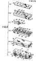
- the magnetic head is produced by the process to be described below with reference to Figs. 3 (a) to (f).
- a highly magnetically permeable material such as sendust or the like is machined to prepare a comb-like magnetic plate 23 as shown in Fig. 3 (a).
- the plate 23 has a highly planar surface.
- the magnetic plate 23 is joined to a nonmagnetic plate 14 which is already provided with a plurality of terminals 40 at its rear portion.
- the magnetic plate 23 can be joined to the nonmagnetic plate 14 by frit or an organic resin adhesive of the epoxy or polyamide type.
- the magnetic plate 23 shown in Fig. 3 (b) is cut along the phantom lines B, B to remove the portion between the lines on the plate 14, and a widthwise groove 24 is formed in the plate 23 to obtain a single elongated ridge 32 and a plurality of projections 33 made integral with the ridge by a thin stepped portion 30 as shown in Fig. 3 (c) and (d).
- a spacer 15 of SiO 2 is formed on the surface of the ridge 32 to a thickness of 0.2 to 0.3 pm by vacuum evaporation.
- a coil 4 is provided around each projection 33, and each end of the coil wire is connected to the terminal 40 (see Fig. 3 (d)).
- a magnetic plate 27 having approximately the same shape as the magnetic plate 23 of.Fig. 3 (a) and secured to a nonmagnetic plate 16 is prepared as a block, which is placed over the block of Fig. 3 (d) and bonded thereto with frit or organic resin adhesive to obtain an assembly as illustrated.
- Recesses 17 are then formed in the front side of the assembly at twice the pitch of the projections 33 as shown in Fig. 3 (f), whereby protrusions 18 are formed between the recesses 17.
- the protrusion 18 is aligned with the center line between the pair of adjacent projections 33 and 33 as seen in Fig. 2.
- a cutout 11 extending toward the rear side of the assembly beyond the groove 24 is formed in each protrusion 17, and a shield member 12 is fitted into the cutout 11.
- the cutouts 11 may be formed before forming the recesses 18.
- the cutouts 11 are 40 ⁇ m in width and about 400 ⁇ m in depth. Consequently, the magnetic plate 23 can be divided into a plurality of magnetic pieces each having two projections 33 (see Fig. 2).
- the shield member 12 may be prepared in the form of a plate conforming to the shape of the cutout 11 and inserted into the cutout.
- the shield member may be formed by admixing a powder of Al, Ag or the like with a resin, injecting the mixture into the cutout 11 and solidifying the mixture.
- the assembly is cut along the lines A in Fig. 3 (f), whereby a plurality of magnetic heads shown in Fig. 1 are completed at the same time.
- the nonmagnetic plates 14, 16 serve as the base plates 1, 10, and the magnetic plates 23, 27 provide the magnetic cores 2, 20, 21 and 23.
- the ridge 32 and the projections 33 of the'magnetic plate 23 respectively provide the heads 31 and stud portions 3 of the magnetic cores 20, 22.
- each magnetic head is finished by polishing, and the surface of the head to be in sliding contact with the record medium is finished to a predetermined outwardly curved surface.
- the magnetic cores 2, 20 or 21, 22 form a closed magnetic circuit including the stud portion 3, bringing the gap Gl or G2 into operation.
- the nonmagnetic spacer 15 providing the gaps Gl and G2 is formed on the single magnetic plate 23 shown in Figs. 3 (a) to (d), and the assembly is cut into magnetic heads in the step shown in Fig. 3 (f), with the spacer portions of each pair of head chips 25, 26 remaining in fixed position relative to each other.
- the two gaps Gl and G2 can be positioned accurately on a plane, whereby the positioning error involved in the conventional assembling procedure is avoidable.
- the process is simple and achieves remarkably improved productivity.
- the amount of head depth can be set to an optimum value. This gives a prolonged life to the magnetic head.
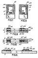
- Figs. 4 to 12 show other embodiments wherein the coil 4 formed around the projection 33 in the step shown in Fig. 3 (d) is replaced by a sheet-like coil 4 which is formed by spiralling a conductor within the plane of a flexible base film and fixing the winding to the film.
- Fig. 4 shows the sheet-like coil 4 as fitted around the projection 33.
- the coil 4 has a thickness smaller than the height (e.g. 200 ⁇ m) of the projection 33, is formed with a centeral hole 51 for the projection to fit in and is integrally provided with terminals 43, 43.
- the sheet-like coil 4 comprises a flexible base sheet 5 made of an insulating material and having a thickness of about 30 ⁇ m, a conductor 44 up to 10 ⁇ m in thickness and spiralled around the hole 51 on the base film 5, and an insulation film 50 about 10 ⁇ m in thickness and covering the conductor 44.
- the inner end of the condcutor 44 is electrically connected to one terminal 43 by a connector 52, while the other end thereof is electrically connected to the other terminal 43.
- Polyester, polyamide or the like is usable for forming the base film 5.
- the conductor 44 is formed as a strip from Cu or Ag by patterning.
- the coil is up to 10 ⁇ m in the width of the conductor 44 and in the conductor-to-conductor spacing.
- the number of turns of the coil which is optional, is for example four in the case of the illustrated embodiment.
- the sheet coil 4 can be produced at a low cost in quantities. Since the sheet-like coil 4 has an overall thickness of up to 70 ⁇ m which is sufficiently smaller than the height (for example, 100 ⁇ m) of the projection 33, the magnetic plates 23 and 27 can be joined together by the step of Fig. 3 (e) without any trouble.
- the coil terminals 40 shown in Fig. 2 can be dispensed with.
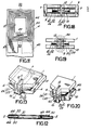
- Figs. 7 to 12 show embodiments wherein conductors 44 are provided in two layers.
- symmetric coils provide a pair of coil half segments 45 and 46, which are joined together as superposed on each other as seen in Fig. 9.
- the inner ends of conductors 44 are exposed on the upper or lower surfaces of the coil half segments 45, 46 to form connecting portions 47, 48, which are electrically connected together, with the segments joined together as ! seen in Fig. 9.
- the two coil half segments 45, 46 form a sheet-like coil 4.
- Fig. 10 shows another sheet-like coil 4 which is obtained by preparing two coil half segments 45 shown in Fig. 7, inverting one of the segments 45 and superposing the segment on the other segment 45.
- Figs. 11 and 12 show another sheet-like coil 4 which comprises a conductor 44 provided on each surface of a single base film 5 and covered with an insulation film 50.
- the two conductors 44 are connected together at a connection 49.
- the coil is mountable on the magnetic core 20 or 22 merely by fitting the coil to the stud portion 3 placing the coil in a space between studs without the necessity of winding a conductor around the stud portion 3. This achieves remarkably improved productivity. Further because the conductor 44 is fully protected by the base film 5 and the insulation film 50, the conductor is free of an insulation breakdown and therefore of short-circuiting during manufacture.
- the sheet-like coil 4 is not limited to the single-or two-layer structure described but can be of a multilayer structure comprising three or more layers, whereby the coil can be given an increased number of turns.
- Fig. 13 shows'a magnetic head wherein the pair of gaps Gl and G2 are magnetically insulated from each other more effectively.
- the width of the cutout 11 needs to be set to about 40 pm in view of the standard for the pitch of tracks. In this case, the limit to the depth of the cutout 11 is 400 pm. Accordingly, magnetic insulation at rear portion of the magnetic head including coils becomes insufficient, which renders cross talk between channels at rear portion of the magnetic head.
- a shield plate 6 opposed to the shield member 12 is inserted between the base plates 1, 10 to separate the space between the two stud portions 3, 3.
- the process for producing this magnetic head includes the steps shown in Figs. 14 (a) and (b) and corresponding to those of Figs. 3 (b) and (f).
- the nonmagnetic plate 14 shown in Fig. 3 (b) is formed in its upper surface with grooves 60 extending from its rear end toward the magnetic plate 23 so as to oppose to the shield members 12.
- the nonmagnetic plate 16 shown in Fig. 3 (e) is also formed in its inner surface with grooves (not shown) opposed to the grooves 60.
- shield plates 6 separately prepared are inserted into the assembly along the grooves 60 and secured to the non- magnetic plates 14, 16. The assembly is thereafter cut along the broken lines A shown, whereby magnetic heads like the one shown in Fig. 13 are completed.
- a resin containing Ag or the like can be provided in the grooves and in the vicinity thereof as in the case of the front shield member 12 to achieve the same effect as the shield plate 6.
- the pair of head chips 25, 26 are magnetically shielded fully by the shield member 12 and the shield plate 6 over the area of from the heads 31 to the stud portions 3, so that cross talk can be prevented more sufficiently.
- Figs. 15 to 17 show another magnetic head wherein two base plates 1 and 10 are made of a magnetic metal material, such as sendust , having approximately the same mechanical properties as the magnetic cores.
- the opposite head chips 25, 26 are magnetically shielded from each other with improved effectiveness, and the magnetic head is improved in mechanical strength and reliability.
- each of the base plates 1 and 10 of sendust has an electromagnetic shield layer 80 in the form of Ag film (1.6 x 10 -8 ohm-cm in specific resistivity) and formed over the inner surface thereof, and an insulation layer 8 in the form of an SiO 2 film ( at least 10 15 ohm-cm in specific resistivity) is formed over the layer 80.
- Magnetic cores 2, 21 (20, 22) are fixedly provided on the upper surface of the insulation layer 8.
- Cu (1.7 x 10 -8 ohm-cm in specific resistivity) is usable for the shield layer 80. In either case, a highly electrically conductive material is useful.
- the magnetic plates 14 and 23 for forming them can be bonded not only by frit or organic resin adhesive but also by silver or like soldering or brazing metal.
- the base plates 1, 10 are made of a nonmagnetic nonmetal material, such as ceramic or the like
- the difference in workability between the material of the base plates 1, 10 and that of the magnetic cores 2, 20, 21, 22 makes it difficult to work the assembly of such plates and cores by a grindstone or abrasive device.
- sendust material is 15 - 20 x 10 -6 / °c
- ceramic materials are 8 - 13 x 10 -6 / °C in coefficient of expansion.
- the assembly in the machining step of Fig. 3 (f) to be performed for the magnetic head of Fig. 15, the assembly can be easily worked, for example, by a thin abrasive blade of boronnitride (BN) type, because the magnetic plates 14, 16 and the magnetic plates 23, 27 are both metal. Moreover, since there is little or no difference between the magnetic plate 14 and the magnetic plate 23 in coefficient of thermal expansion, no deformation or separation occurs during production unlike the above-stated case. Further because the plates to be bonded together can be heated to a higher temperature, a glass material, silver brazing material or like bonding agent of higher bond strength is usable. This gives higher reliability to the production process.
- BN boronnitride
- Fig. 20 shows another magnetic head wherein the base plates 1 and 10 are made of a nonmagnetic metal material to magnetically shield the two head chips 25 and 26 more effectively and give improved mechanical strength and reliability to the head.
- the base plate 10 is formed with an insulation layer 81 over the rear half of its inner surface where coil terminals 40 are to be fixedly provided.
- the process for producing the magnetic head includes the steps shown in Fig. 21 (a) and (b) and corre- spon d ing to the step of Fig. 3 (b).
- a magnetic plate 23 is bonded to the nonmagnetic plate 14.
- the base plates 1 and 10 of the magnetic head shown in Fig. 20 are made of metal material as is the case with the magnetic head of Fig. 15, so that the magnetic plate 23 or the nonmagnetic plate 14 will not deform or separate during the production process, and the parts are easy to machine.
- the magnetic head has the same advantages as the head of Fig. 15.
Landscapes
- Engineering & Computer Science (AREA)
- Manufacturing & Machinery (AREA)
- Magnetic Heads (AREA)
Applications Claiming Priority (10)
| Application Number | Priority Date | Filing Date | Title |
|---|---|---|---|
| JP59229807A JPS61110318A (ja) | 1984-10-31 | 1984-10-31 | 磁気ヘツド及びその製造方法 |
| JP229807/84 | 1984-10-31 | ||
| JP60102071A JPS61283014A (ja) | 1985-05-14 | 1985-05-14 | 磁気ヘツドの製造方法 |
| JP102071/85 | 1985-05-14 | ||
| JP104248/85 | 1985-05-16 | ||
| JP60104248A JPS61283015A (ja) | 1985-05-16 | 1985-05-16 | 磁気ヘツド |
| JP60106383A JPS61283017A (ja) | 1985-05-17 | 1985-05-17 | 磁気ヘツド |
| JP106382/85 | 1985-05-17 | ||
| JP60106382A JPS61283016A (ja) | 1985-05-17 | 1985-05-17 | 磁気ヘツド及びその製造方法 |
| JP106383/85 | 1985-05-17 |
Publications (3)
| Publication Number | Publication Date |
|---|---|
| EP0180218A2 true EP0180218A2 (de) | 1986-05-07 |
| EP0180218A3 EP0180218A3 (en) | 1987-11-25 |
| EP0180218B1 EP0180218B1 (de) | 1991-02-06 |
Family
ID=27526078
Family Applications (1)
| Application Number | Title | Priority Date | Filing Date |
|---|---|---|---|
| EP85113846A Expired - Lifetime EP0180218B1 (de) | 1984-10-31 | 1985-10-31 | Magnetkopf und Herstellungsverfahren |
Country Status (6)
| Country | Link |
|---|---|
| US (2) | US4719527A (de) |
| EP (1) | EP0180218B1 (de) |
| KR (1) | KR930008776B1 (de) |
| CN (1) | CN85108011B (de) |
| CA (1) | CA1249658A (de) |
| DE (1) | DE3581694D1 (de) |
Cited By (1)
| Publication number | Priority date | Publication date | Assignee | Title |
|---|---|---|---|---|
| US4946344A (en) * | 1987-12-08 | 1990-08-07 | B.V. Machinefabriek Figee | General cargo crane |
Families Citing this family (15)
| Publication number | Priority date | Publication date | Assignee | Title |
|---|---|---|---|---|
| JPH0664709B2 (ja) * | 1984-01-26 | 1994-08-22 | キヤノン株式会社 | 薄膜磁気ヘツド |
| US4883950A (en) * | 1987-05-23 | 1989-11-28 | The Furukawa Electric Co., Ltd. | Composite magnetic and optical head |
| JPH01182908A (ja) * | 1988-01-13 | 1989-07-20 | Hitachi Ltd | 薄膜磁気ヘツド |
| US5293360A (en) * | 1989-03-09 | 1994-03-08 | Canon Kabushiki Kaisha | Magnetic field generating device |
| JP2611867B2 (ja) * | 1990-10-25 | 1997-05-21 | 富士写真フイルム株式会社 | 改良されたコイル導体層を備える薄膜磁気ヘッド |
| EP0725387B1 (de) * | 1991-04-19 | 1998-09-02 | Sony Corporation | Magnetkopfherstellungsverfahren |
| JPH04344311A (ja) * | 1991-05-21 | 1992-11-30 | Ngk Insulators Ltd | 薄膜磁気回路基板及びそれを用いた磁気ヘッド |
| US5778514A (en) * | 1993-01-06 | 1998-07-14 | Das Devices, Inc. | Method for forming a transducing head |
| EP0631275B1 (de) * | 1993-06-28 | 2002-09-04 | Tandberg Data Asa | Kopfanordnung mit geringem Abstand zwischen Aufnahme/Wiedergabeköpfe |
| JPH07169015A (ja) * | 1993-12-10 | 1995-07-04 | Sony Corp | 磁気ヘッド |
| JP3463759B2 (ja) * | 1993-12-29 | 2003-11-05 | ソニー株式会社 | 磁気ヘッド及びその製造方法 |
| US6963464B2 (en) * | 2000-10-26 | 2005-11-08 | Hitachi Global Storage Technologies Japan, Ltd. | Magnetic head heating element in a disk drive |
| US7403354B2 (en) * | 2005-02-28 | 2008-07-22 | Seagate Technology Llc | Two layer writer heater using writer as one current lead |
| JP5542898B2 (ja) * | 2012-10-24 | 2014-07-09 | Jx日鉱日石金属株式会社 | カメラモジュール及びチタン銅箔 |
| US20210375536A1 (en) * | 2017-11-06 | 2021-12-02 | United States Department Of Energy | Mixed material magnetic core for shielding of eddy current induced excess losses |
Family Cites Families (17)
| Publication number | Priority date | Publication date | Assignee | Title |
|---|---|---|---|---|
| DE1160502B (de) * | 1959-01-10 | 1964-01-02 | Grundig Max | Mehrspurmagnetkopf-Anordnung |
| US3412216A (en) * | 1965-01-13 | 1968-11-19 | Headmaster Electronics Corp | Combination record-reproduce and erase magnetic head |
| US3685144A (en) * | 1967-09-18 | 1972-08-22 | Ncr Co | Method of making a magnetic transducer |
| DE1800384A1 (de) * | 1968-10-01 | 1970-05-21 | Bogen Gmbh W | Magnetkopf mit integrierter Abschirmung |
| US3613228A (en) * | 1969-07-02 | 1971-10-19 | Ibm | Manufacture of multielement magnetic head assemblies |
| US3700827A (en) * | 1970-01-31 | 1972-10-24 | Nippon Electric Co | Magnetic head including thin magnetic film separated by a gap spacer |
| GB1358084A (en) * | 1970-12-11 | 1974-06-26 | Ibm | Multi-gap magnetic transducers and methods of making them |
| US3829896A (en) * | 1972-11-08 | 1974-08-13 | Ibm | Bias means for batch fabricated magnetic head and method of manufacture thereof |
| US4124874A (en) * | 1976-09-02 | 1978-11-07 | Bell & Howell Company | Magnetic information transducer assembly |
| GB2050699B (en) * | 1977-12-13 | 1982-10-20 | Fujitsu Ltd | Thin-film coil producing method |
| JPS5620A (en) * | 1979-06-12 | 1981-01-06 | Fujitsu Ltd | Magnetic head |
| US4357640A (en) * | 1980-10-24 | 1982-11-02 | Nortronics Company, Inc. | Thin film magnetic transducer |
| FR2494952B1 (fr) * | 1980-11-27 | 1986-06-06 | Bull Sa | Transducteur magnetoresistant de lecture d'un support d'enregistrement a haute densite d'informations |
| US4396967A (en) * | 1981-04-13 | 1983-08-02 | International Business Machines Corporation | Multielement magnetic head assembly |
| JPS58130419A (ja) * | 1982-01-29 | 1983-08-03 | Victor Co Of Japan Ltd | 複合型磁気ヘツドコア |
| JPS595413A (ja) * | 1982-07-01 | 1984-01-12 | Nec Home Electronics Ltd | バルク型磁気ヘツド |
| JPH0664714B2 (ja) * | 1983-11-25 | 1994-08-22 | 株式会社東芝 | 薄膜磁気ヘッド |
-
1985
- 1985-10-30 CA CA000494243A patent/CA1249658A/en not_active Expired
- 1985-10-30 KR KR1019850008030A patent/KR930008776B1/ko not_active Expired - Fee Related
- 1985-10-30 US US06/793,007 patent/US4719527A/en not_active Expired - Fee Related
- 1985-10-31 CN CN85108011A patent/CN85108011B/zh not_active Expired
- 1985-10-31 DE DE8585113846T patent/DE3581694D1/de not_active Expired - Fee Related
- 1985-10-31 EP EP85113846A patent/EP0180218B1/de not_active Expired - Lifetime
-
1987
- 1987-10-13 US US07/106,841 patent/US4774755A/en not_active Expired - Fee Related
Cited By (1)
| Publication number | Priority date | Publication date | Assignee | Title |
|---|---|---|---|---|
| US4946344A (en) * | 1987-12-08 | 1990-08-07 | B.V. Machinefabriek Figee | General cargo crane |
Also Published As
| Publication number | Publication date |
|---|---|
| CN85108011B (zh) | 1988-04-20 |
| DE3581694D1 (de) | 1991-03-14 |
| US4719527A (en) | 1988-01-12 |
| KR930008776B1 (ko) | 1993-09-15 |
| US4774755A (en) | 1988-10-04 |
| KR860003581A (ko) | 1986-05-26 |
| CA1249658A (en) | 1989-01-31 |
| EP0180218A3 (en) | 1987-11-25 |
| CN85108011A (zh) | 1986-04-10 |
| EP0180218B1 (de) | 1991-02-06 |
Similar Documents
| Publication | Publication Date | Title |
|---|---|---|
| EP0180218B1 (de) | Magnetkopf und Herstellungsverfahren | |
| CA1147055A (en) | Magnetic transducer head and method of manufacturing the same | |
| EP0233086A2 (de) | Dünnschichtmagnetkopf | |
| US4071868A (en) | Narrow track MR head with side shields | |
| US4713709A (en) | Twin head for electronic still camera and a method for making the same | |
| EP0062739B1 (de) | Mehrelement-Magnetkopfeinheit und Verfahren zu deren Herstellung | |
| US4860140A (en) | Magnetic head closure having ferrite substrate and closure and conductive thin film coil deposited in recess of substantially same shape in ferrite substrate | |
| US5497283A (en) | Magnetic head having coil bobbins separated from a terminal assembly | |
| US4821134A (en) | Magnetic alloy R/W head with centrally pinched and end slotted core | |
| US4514776A (en) | Magnetic head and method of manufacturing the same | |
| US5267392A (en) | Method of manufacturing a laminated high frequency magnetic transducer | |
| US5390062A (en) | Thin-film magnetic circuit board and magnetic head using the same | |
| KR930000067B1 (ko) | 자기헤드 | |
| EP0061069B1 (de) | Magnetischer Wandler | |
| US6038109A (en) | Magnetic head and method of manufacturing the same | |
| JP2646746B2 (ja) | 磁気ヘッド及びその製造方法 | |
| US5883766A (en) | Magnetic head with groove positioned to identify head orientation | |
| KR960005113B1 (ko) | 박막자기헤드 | |
| JPH0232686B2 (de) | ||
| JPH0561681B2 (de) | ||
| KR19990023461A (ko) | 자기 헤드 및 그 제조 방법 | |
| JPS6334708A (ja) | 磁気ヘツドおよびその製造方法 | |
| JPH04167205A (ja) | 磁気ヘッド | |
| JPH0757214A (ja) | ラミネート型磁気ヘッドおよびその製造方法 | |
| JPS63124206A (ja) | 磁気ヘツド |
Legal Events
| Date | Code | Title | Description |
|---|---|---|---|
| PUAI | Public reference made under article 153(3) epc to a published international application that has entered the european phase |
Free format text: ORIGINAL CODE: 0009012 |
|
| AK | Designated contracting states |
Kind code of ref document: A2 Designated state(s): CH DE FR GB LI NL |
|
| PUAL | Search report despatched |
Free format text: ORIGINAL CODE: 0009013 |
|
| AK | Designated contracting states |
Kind code of ref document: A3 Designated state(s): CH DE FR GB LI NL |
|
| 17P | Request for examination filed |
Effective date: 19880318 |
|
| 17Q | First examination report despatched |
Effective date: 19890919 |
|
| GRAA | (expected) grant |
Free format text: ORIGINAL CODE: 0009210 |
|
| AK | Designated contracting states |
Kind code of ref document: B1 Designated state(s): CH DE FR GB LI NL |
|
| ET | Fr: translation filed | ||
| REF | Corresponds to: |
Ref document number: 3581694 Country of ref document: DE Date of ref document: 19910314 |
|
| PLBE | No opposition filed within time limit |
Free format text: ORIGINAL CODE: 0009261 |
|
| STAA | Information on the status of an ep patent application or granted ep patent |
Free format text: STATUS: NO OPPOSITION FILED WITHIN TIME LIMIT |
|
| 26N | No opposition filed | ||
| PGFP | Annual fee paid to national office [announced via postgrant information from national office to epo] |
Ref country code: FR Payment date: 19981009 Year of fee payment: 14 |
|
| PGFP | Annual fee paid to national office [announced via postgrant information from national office to epo] |
Ref country code: NL Payment date: 19981028 Year of fee payment: 14 |
|
| PGFP | Annual fee paid to national office [announced via postgrant information from national office to epo] |
Ref country code: GB Payment date: 19981106 Year of fee payment: 14 Ref country code: DE Payment date: 19981106 Year of fee payment: 14 |
|
| PGFP | Annual fee paid to national office [announced via postgrant information from national office to epo] |
Ref country code: CH Payment date: 19981113 Year of fee payment: 14 |
|
| PG25 | Lapsed in a contracting state [announced via postgrant information from national office to epo] |
Ref country code: LI Free format text: LAPSE BECAUSE OF NON-PAYMENT OF DUE FEES Effective date: 19991031 Ref country code: GB Free format text: LAPSE BECAUSE OF NON-PAYMENT OF DUE FEES Effective date: 19991031 Ref country code: CH Free format text: LAPSE BECAUSE OF NON-PAYMENT OF DUE FEES Effective date: 19991031 |
|
| PG25 | Lapsed in a contracting state [announced via postgrant information from national office to epo] |
Ref country code: NL Free format text: LAPSE BECAUSE OF NON-PAYMENT OF DUE FEES Effective date: 20000501 |
|
| REG | Reference to a national code |
Ref country code: CH Ref legal event code: PL |
|
| GBPC | Gb: european patent ceased through non-payment of renewal fee |
Effective date: 19991031 |
|
| PG25 | Lapsed in a contracting state [announced via postgrant information from national office to epo] |
Ref country code: FR Free format text: LAPSE BECAUSE OF NON-PAYMENT OF DUE FEES Effective date: 20000630 |
|
| NLV4 | Nl: lapsed or anulled due to non-payment of the annual fee |
Effective date: 20000501 |
|
| PG25 | Lapsed in a contracting state [announced via postgrant information from national office to epo] |
Ref country code: DE Free format text: LAPSE BECAUSE OF NON-PAYMENT OF DUE FEES Effective date: 20000801 |
|
| REG | Reference to a national code |
Ref country code: FR Ref legal event code: ST |