EP0214610B1 - Epitaktische Gallium-Arsenid-Halbleiterscheibe und Verfahren zu ihrer Herstellung - Google Patents
Epitaktische Gallium-Arsenid-Halbleiterscheibe und Verfahren zu ihrer Herstellung Download PDFInfo
- Publication number
- EP0214610B1 EP0214610B1 EP19860112178 EP86112178A EP0214610B1 EP 0214610 B1 EP0214610 B1 EP 0214610B1 EP 19860112178 EP19860112178 EP 19860112178 EP 86112178 A EP86112178 A EP 86112178A EP 0214610 B1 EP0214610 B1 EP 0214610B1
- Authority
- EP
- European Patent Office
- Prior art keywords
- layer
- gaas
- substrate
- gap
- gaasp
- Prior art date
- Legal status (The legal status is an assumption and is not a legal conclusion. Google has not performed a legal analysis and makes no representation as to the accuracy of the status listed.)
- Expired - Lifetime
Links
Images


Classifications
-
- H—ELECTRICITY
- H10—SEMICONDUCTOR DEVICES; ELECTRIC SOLID-STATE DEVICES NOT OTHERWISE PROVIDED FOR
- H10F—INORGANIC SEMICONDUCTOR DEVICES SENSITIVE TO INFRARED RADIATION, LIGHT, ELECTROMAGNETIC RADIATION OF SHORTER WAVELENGTH OR CORPUSCULAR RADIATION
- H10F10/00—Individual photovoltaic cells, e.g. solar cells
- H10F10/10—Individual photovoltaic cells, e.g. solar cells having potential barriers
- H10F10/14—Photovoltaic cells having only PN homojunction potential barriers
- H10F10/144—Photovoltaic cells having only PN homojunction potential barriers comprising only Group III-V materials, e.g. GaAs,AlGaAs, or InP photovoltaic cells
-
- H—ELECTRICITY
- H10—SEMICONDUCTOR DEVICES; ELECTRIC SOLID-STATE DEVICES NOT OTHERWISE PROVIDED FOR
- H10D—INORGANIC ELECTRIC SEMICONDUCTOR DEVICES
- H10D62/00—Semiconductor bodies, or regions thereof, of devices having potential barriers
- H10D62/40—Crystalline structures
- H10D62/405—Orientations of crystalline planes
-
- H—ELECTRICITY
- H10—SEMICONDUCTOR DEVICES; ELECTRIC SOLID-STATE DEVICES NOT OTHERWISE PROVIDED FOR
- H10D—INORGANIC ELECTRIC SEMICONDUCTOR DEVICES
- H10D62/00—Semiconductor bodies, or regions thereof, of devices having potential barriers
- H10D62/80—Semiconductor bodies, or regions thereof, of devices having potential barriers characterised by the materials
- H10D62/82—Heterojunctions
-
- H—ELECTRICITY
- H10—SEMICONDUCTOR DEVICES; ELECTRIC SOLID-STATE DEVICES NOT OTHERWISE PROVIDED FOR
- H10F—INORGANIC SEMICONDUCTOR DEVICES SENSITIVE TO INFRARED RADIATION, LIGHT, ELECTROMAGNETIC RADIATION OF SHORTER WAVELENGTH OR CORPUSCULAR RADIATION
- H10F30/00—Individual radiation-sensitive semiconductor devices in which radiation controls the flow of current through the devices, e.g. photodetectors
- H10F30/20—Individual radiation-sensitive semiconductor devices in which radiation controls the flow of current through the devices, e.g. photodetectors the devices having potential barriers, e.g. phototransistors
- H10F30/21—Individual radiation-sensitive semiconductor devices in which radiation controls the flow of current through the devices, e.g. photodetectors the devices having potential barriers, e.g. phototransistors the devices being sensitive to infrared, visible or ultraviolet radiation
- H10F30/22—Individual radiation-sensitive semiconductor devices in which radiation controls the flow of current through the devices, e.g. photodetectors the devices having potential barriers, e.g. phototransistors the devices being sensitive to infrared, visible or ultraviolet radiation the devices having only one potential barrier, e.g. photodiodes
- H10F30/223—Individual radiation-sensitive semiconductor devices in which radiation controls the flow of current through the devices, e.g. photodetectors the devices having potential barriers, e.g. phototransistors the devices being sensitive to infrared, visible or ultraviolet radiation the devices having only one potential barrier, e.g. photodiodes the potential barrier being a PIN barrier
-
- H—ELECTRICITY
- H10—SEMICONDUCTOR DEVICES; ELECTRIC SOLID-STATE DEVICES NOT OTHERWISE PROVIDED FOR
- H10F—INORGANIC SEMICONDUCTOR DEVICES SENSITIVE TO INFRARED RADIATION, LIGHT, ELECTROMAGNETIC RADIATION OF SHORTER WAVELENGTH OR CORPUSCULAR RADIATION
- H10F71/00—Manufacture or treatment of devices covered by this subclass
- H10F71/127—The active layers comprising only Group III-V materials, e.g. GaAs or InP
-
- H—ELECTRICITY
- H10—SEMICONDUCTOR DEVICES; ELECTRIC SOLID-STATE DEVICES NOT OTHERWISE PROVIDED FOR
- H10H—INORGANIC LIGHT-EMITTING SEMICONDUCTOR DEVICES HAVING POTENTIAL BARRIERS
- H10H20/00—Individual inorganic light-emitting semiconductor devices having potential barriers, e.g. light-emitting diodes [LED]
- H10H20/01—Manufacture or treatment
- H10H20/011—Manufacture or treatment of bodies, e.g. forming semiconductor layers
- H10H20/013—Manufacture or treatment of bodies, e.g. forming semiconductor layers having light-emitting regions comprising only Group III-V materials
- H10H20/0133—Manufacture or treatment of bodies, e.g. forming semiconductor layers having light-emitting regions comprising only Group III-V materials with a substrate not being Group III-V materials
-
- H—ELECTRICITY
- H10—SEMICONDUCTOR DEVICES; ELECTRIC SOLID-STATE DEVICES NOT OTHERWISE PROVIDED FOR
- H10P—GENERIC PROCESSES OR APPARATUS FOR THE MANUFACTURE OR TREATMENT OF DEVICES COVERED BY CLASS H10
- H10P14/00—Formation of materials, e.g. in the shape of layers or pillars
- H10P14/20—Formation of materials, e.g. in the shape of layers or pillars of semiconductor materials
- H10P14/24—Formation of materials, e.g. in the shape of layers or pillars of semiconductor materials using chemical vapour deposition [CVD]
-
- H—ELECTRICITY
- H10—SEMICONDUCTOR DEVICES; ELECTRIC SOLID-STATE DEVICES NOT OTHERWISE PROVIDED FOR
- H10P—GENERIC PROCESSES OR APPARATUS FOR THE MANUFACTURE OR TREATMENT OF DEVICES COVERED BY CLASS H10
- H10P14/00—Formation of materials, e.g. in the shape of layers or pillars
- H10P14/20—Formation of materials, e.g. in the shape of layers or pillars of semiconductor materials
- H10P14/29—Formation of materials, e.g. in the shape of layers or pillars of semiconductor materials characterised by the substrates
- H10P14/2901—Materials
- H10P14/2902—Materials being Group IVA materials
- H10P14/2905—Silicon, silicon germanium or germanium
-
- H—ELECTRICITY
- H10—SEMICONDUCTOR DEVICES; ELECTRIC SOLID-STATE DEVICES NOT OTHERWISE PROVIDED FOR
- H10P—GENERIC PROCESSES OR APPARATUS FOR THE MANUFACTURE OR TREATMENT OF DEVICES COVERED BY CLASS H10
- H10P14/00—Formation of materials, e.g. in the shape of layers or pillars
- H10P14/20—Formation of materials, e.g. in the shape of layers or pillars of semiconductor materials
- H10P14/29—Formation of materials, e.g. in the shape of layers or pillars of semiconductor materials characterised by the substrates
- H10P14/2926—Crystal orientations
-
- H—ELECTRICITY
- H10—SEMICONDUCTOR DEVICES; ELECTRIC SOLID-STATE DEVICES NOT OTHERWISE PROVIDED FOR
- H10P—GENERIC PROCESSES OR APPARATUS FOR THE MANUFACTURE OR TREATMENT OF DEVICES COVERED BY CLASS H10
- H10P14/00—Formation of materials, e.g. in the shape of layers or pillars
- H10P14/20—Formation of materials, e.g. in the shape of layers or pillars of semiconductor materials
- H10P14/32—Formation of materials, e.g. in the shape of layers or pillars of semiconductor materials characterised by intermediate layers between substrates and deposited layers
- H10P14/3202—Materials thereof
- H10P14/3214—Materials thereof being Group IIIA-VA semiconductors
- H10P14/3218—Phosphides
-
- H—ELECTRICITY
- H10—SEMICONDUCTOR DEVICES; ELECTRIC SOLID-STATE DEVICES NOT OTHERWISE PROVIDED FOR
- H10P—GENERIC PROCESSES OR APPARATUS FOR THE MANUFACTURE OR TREATMENT OF DEVICES COVERED BY CLASS H10
- H10P14/00—Formation of materials, e.g. in the shape of layers or pillars
- H10P14/20—Formation of materials, e.g. in the shape of layers or pillars of semiconductor materials
- H10P14/32—Formation of materials, e.g. in the shape of layers or pillars of semiconductor materials characterised by intermediate layers between substrates and deposited layers
- H10P14/3202—Materials thereof
- H10P14/3214—Materials thereof being Group IIIA-VA semiconductors
- H10P14/3221—Arsenides
-
- H—ELECTRICITY
- H10—SEMICONDUCTOR DEVICES; ELECTRIC SOLID-STATE DEVICES NOT OTHERWISE PROVIDED FOR
- H10P—GENERIC PROCESSES OR APPARATUS FOR THE MANUFACTURE OR TREATMENT OF DEVICES COVERED BY CLASS H10
- H10P14/00—Formation of materials, e.g. in the shape of layers or pillars
- H10P14/20—Formation of materials, e.g. in the shape of layers or pillars of semiconductor materials
- H10P14/32—Formation of materials, e.g. in the shape of layers or pillars of semiconductor materials characterised by intermediate layers between substrates and deposited layers
- H10P14/3242—Structure
- H10P14/3244—Layer structure
- H10P14/3251—Layer structure consisting of three or more layers
- H10P14/3252—Alternating layers, e.g. superlattice
-
- H—ELECTRICITY
- H10—SEMICONDUCTOR DEVICES; ELECTRIC SOLID-STATE DEVICES NOT OTHERWISE PROVIDED FOR
- H10P—GENERIC PROCESSES OR APPARATUS FOR THE MANUFACTURE OR TREATMENT OF DEVICES COVERED BY CLASS H10
- H10P14/00—Formation of materials, e.g. in the shape of layers or pillars
- H10P14/20—Formation of materials, e.g. in the shape of layers or pillars of semiconductor materials
- H10P14/34—Deposited materials, e.g. layers
- H10P14/3402—Deposited materials, e.g. layers characterised by the chemical composition
- H10P14/3414—Deposited materials, e.g. layers characterised by the chemical composition being group IIIA-VIA materials
- H10P14/3421—Arsenides
-
- H—ELECTRICITY
- H10—SEMICONDUCTOR DEVICES; ELECTRIC SOLID-STATE DEVICES NOT OTHERWISE PROVIDED FOR
- H10P—GENERIC PROCESSES OR APPARATUS FOR THE MANUFACTURE OR TREATMENT OF DEVICES COVERED BY CLASS H10
- H10P14/00—Formation of materials, e.g. in the shape of layers or pillars
- H10P14/20—Formation of materials, e.g. in the shape of layers or pillars of semiconductor materials
- H10P14/34—Deposited materials, e.g. layers
- H10P14/3438—Doping during depositing
- H10P14/3441—Conductivity type
-
- Y—GENERAL TAGGING OF NEW TECHNOLOGICAL DEVELOPMENTS; GENERAL TAGGING OF CROSS-SECTIONAL TECHNOLOGIES SPANNING OVER SEVERAL SECTIONS OF THE IPC; TECHNICAL SUBJECTS COVERED BY FORMER USPC CROSS-REFERENCE ART COLLECTIONS [XRACs] AND DIGESTS
- Y02—TECHNOLOGIES OR APPLICATIONS FOR MITIGATION OR ADAPTATION AGAINST CLIMATE CHANGE
- Y02E—REDUCTION OF GREENHOUSE GAS [GHG] EMISSIONS, RELATED TO ENERGY GENERATION, TRANSMISSION OR DISTRIBUTION
- Y02E10/00—Energy generation through renewable energy sources
- Y02E10/50—Photovoltaic [PV] energy
- Y02E10/544—Solar cells from Group III-V materials
-
- Y—GENERAL TAGGING OF NEW TECHNOLOGICAL DEVELOPMENTS; GENERAL TAGGING OF CROSS-SECTIONAL TECHNOLOGIES SPANNING OVER SEVERAL SECTIONS OF THE IPC; TECHNICAL SUBJECTS COVERED BY FORMER USPC CROSS-REFERENCE ART COLLECTIONS [XRACs] AND DIGESTS
- Y10—TECHNICAL SUBJECTS COVERED BY FORMER USPC
- Y10S—TECHNICAL SUBJECTS COVERED BY FORMER USPC CROSS-REFERENCE ART COLLECTIONS [XRACs] AND DIGESTS
- Y10S117/00—Single-crystal, oriented-crystal, and epitaxy growth processes; non-coating apparatus therefor
- Y10S117/901—Levitation, reduced gravity, microgravity, space
- Y10S117/902—Specified orientation, shape, crystallography, or size of seed or substrate
-
- Y—GENERAL TAGGING OF NEW TECHNOLOGICAL DEVELOPMENTS; GENERAL TAGGING OF CROSS-SECTIONAL TECHNOLOGIES SPANNING OVER SEVERAL SECTIONS OF THE IPC; TECHNICAL SUBJECTS COVERED BY FORMER USPC CROSS-REFERENCE ART COLLECTIONS [XRACs] AND DIGESTS
- Y10—TECHNICAL SUBJECTS COVERED BY FORMER USPC
- Y10S—TECHNICAL SUBJECTS COVERED BY FORMER USPC CROSS-REFERENCE ART COLLECTIONS [XRACs] AND DIGESTS
- Y10S148/00—Metal treatment
- Y10S148/072—Heterojunctions
-
- Y—GENERAL TAGGING OF NEW TECHNOLOGICAL DEVELOPMENTS; GENERAL TAGGING OF CROSS-SECTIONAL TECHNOLOGIES SPANNING OVER SEVERAL SECTIONS OF THE IPC; TECHNICAL SUBJECTS COVERED BY FORMER USPC CROSS-REFERENCE ART COLLECTIONS [XRACs] AND DIGESTS
- Y10—TECHNICAL SUBJECTS COVERED BY FORMER USPC
- Y10S—TECHNICAL SUBJECTS COVERED BY FORMER USPC CROSS-REFERENCE ART COLLECTIONS [XRACs] AND DIGESTS
- Y10S148/00—Metal treatment
- Y10S148/097—Lattice strain and defects
-
- Y—GENERAL TAGGING OF NEW TECHNOLOGICAL DEVELOPMENTS; GENERAL TAGGING OF CROSS-SECTIONAL TECHNOLOGIES SPANNING OVER SEVERAL SECTIONS OF THE IPC; TECHNICAL SUBJECTS COVERED BY FORMER USPC CROSS-REFERENCE ART COLLECTIONS [XRACs] AND DIGESTS
- Y10—TECHNICAL SUBJECTS COVERED BY FORMER USPC
- Y10S—TECHNICAL SUBJECTS COVERED BY FORMER USPC CROSS-REFERENCE ART COLLECTIONS [XRACs] AND DIGESTS
- Y10S148/00—Metal treatment
- Y10S148/16—Superlattice
-
- Y—GENERAL TAGGING OF NEW TECHNOLOGICAL DEVELOPMENTS; GENERAL TAGGING OF CROSS-SECTIONAL TECHNOLOGIES SPANNING OVER SEVERAL SECTIONS OF THE IPC; TECHNICAL SUBJECTS COVERED BY FORMER USPC CROSS-REFERENCE ART COLLECTIONS [XRACs] AND DIGESTS
- Y10—TECHNICAL SUBJECTS COVERED BY FORMER USPC
- Y10S—TECHNICAL SUBJECTS COVERED BY FORMER USPC CROSS-REFERENCE ART COLLECTIONS [XRACs] AND DIGESTS
- Y10S438/00—Semiconductor device manufacturing: process
- Y10S438/933—Germanium or silicon or Ge-Si on III-V
-
- Y—GENERAL TAGGING OF NEW TECHNOLOGICAL DEVELOPMENTS; GENERAL TAGGING OF CROSS-SECTIONAL TECHNOLOGIES SPANNING OVER SEVERAL SECTIONS OF THE IPC; TECHNICAL SUBJECTS COVERED BY FORMER USPC CROSS-REFERENCE ART COLLECTIONS [XRACs] AND DIGESTS
- Y10—TECHNICAL SUBJECTS COVERED BY FORMER USPC
- Y10S—TECHNICAL SUBJECTS COVERED BY FORMER USPC CROSS-REFERENCE ART COLLECTIONS [XRACs] AND DIGESTS
- Y10S438/00—Semiconductor device manufacturing: process
- Y10S438/938—Lattice strain control or utilization
Definitions
- the present invention relates to semiconductor wafers having an epitaxially grown gallium arsenide layer, useful for fabricating various GaAs compound semiconducting devices, and methods suitable for producing such semiconductor wafers and devices.
- Group III-V compound semiconductors with a gallium arsenide (GaAs) layer have high carrier mobility, direct-gap band structure, and variable nature of band gap and lattice parameter or constant in the case of the compounds consisting of three or four elements. Owing to these characteristics, the Group III-V compound semiconductors have been enjoying expanding industrial applications for fabricating not only a variety of semiconductor elements such as high-speed transistors, laser diodes, light emitting diodes (LED), phototransistors, photodiodes and solar cells, but also integrated circuits incorporating these semiconductor elements.
- An active layer providing such an active element is formed in a monocrystalline substrate of gallium arsenide, by preferential diffusion or ion implantation technique, or alternatively as an epitaxial GaAs layer formed by epitaxy on the GaAs substrate crystal.
- a monocrystalline gallium arsenide (GaAs) substrate suffers from some disadvantages over a monocrystalline silicon (Si) substrate, e.g., more difficulty in obtaining an ingot of a relatively large diameter, higher cost of production, and lower mechanical strength.
- a monocrystalline gallium arsenide substrate there has been an attempt to use a monocrystalline substrate of silicon, since the technologies for producing and processing its ingot are most advanced in the field of semiconductor materials.
- an active layer of gallium arsenide is epitaxially grown or formed by epitaxy on the surface of the monocrystalline silicon substrate.
- the thus obtained semiconductor wafer tends to have a lattice mismatch or dislocation of the epitaxial gallium arsenide active layer and the silicon substrate, and is not satisfactory in crystallinity of the active layer.
- Applied Physics Letters, Vol. 45, August 1985, pages 397-399 discloses GaAs bipolar transistors grown on (100) Si substrates by molecular beam epitaxy. Said Si-substrates are oriented 4° of (100) towards (110) on which a GaAs buffer is grown.
- Applied Physics Letters, Vol. 45, August 15,1984, pages 309-311 discloses the design of a monolithie GaAs/Si diode laser which comprises a Ge-coated Si on which GaAs and AIGaAs layers are epitaxially grown.
- IBM Technical Disclosure Bulletin, Vol. 22, June 1979, page 401, discloses integrated light-emitting devices with silicon LSI circuits comprising a silicon substrate and different semiconductor layers.
- the present inventors have conducted extensive studies and investigations on an intermediate buffer layer to be interposed between the silicon substrate and the epitaxial gallium arsenide layer for accommodating a lattice mismatch therebetween, and on an off angle at which the major surface of the silicon substrate is inclined with respect to a given plane (100) of the crystal.
- the present invention was developed as a result of the above findings of the inventors. According to the invention, there is provided a semiconductor wafer as defined in claim 1.
- the present semiconductor wafer with the epitaxial GaAs layer is suitably produced by a method according to the invention as defined in claim 3.
- the crystallinity of the epitaxial gallium arsenide (GaAs) layer formed on the silicon (Si) substrate was evaluated by measuring the surface roughness of the GaAs layer by a contact-type surface roughness tester, and the value (meV) of photoluminescence full-width at half maximum.
- the specified optimum range (0.5 to 5 degrees) of the off angle of the Si substrate permits the epitaxial GaAs layer according to the invention to have a higher degree of crystallinity, and a smaller, that those of a GaAs layer to be grown on the Si substrate of (100) orientation (commonly used as a major surface on which the GaAs layer is formed).
- the off angle range is preferably between 1° and 3°, and more preferably in the neighborhood of 2°.
- the intermediate layer consists of a single gallium phosphide (GaP) layer.
- the intermediate layer may include at least one superlatice layer.
- the intermediate layer consists of at least one GaP/GaAsP superlattice layer formed on the Si substrate, and at least one GaAsP/GaAs superlattice layer which is formed on the at least one GaP/GaAsP superlattice layer and on which the epitaxial GaAs layer is formed.
- the GaAs layer is formed on the intermediate buffer layers which consist of the Gap layer, the GaP/GaAsP and GaAsP/GaAs superlattice layers, all of these intermediate layers being superposed on each other in the order of description as seen in the direction from the major surface of the Si substrate.
- the provision of these intermediate layers contribute to improved crystallinity of the epitaxial GaAs layer formed on top of the intermediate layers.
- the instant semiconductor wafer using a silicon substrate and an epitaxial gallium arsenide active layer is suitably applied for the fabrication of various high-quality semiconductor elements, integrated circuits, and optical integrated circuits and other hybrid integrated circuits which are combinations of conventional silicon ICs and Ground III-V compound gallium arsenide ICs.
- the instant semiconductor wafer is used for bi-polar transistors, field effect transistors, light emitting diodes, laser diodes, light receiving elements, solar cells, and other semiconductor elements, and is further used for integrated circuits incorporating such semiconductor elements in combination.
- a semiconductor light emitting element and a compound semiconductor device as defined in claim 5 and claim 8 respectively.
- reference numeral 10 designates an n-type monocrystalline silicon (Si) substrate.
- Si monocrystalline silicon
- GaP intermediate gallium phosphide
- GaAs epitaxial gallium arsenide
- the monocrystalline Si substrate 10 has a thickness of 300 micrometers.
- the GaP layer 30 is 0.5 micrometers thick, while the GaAs layer 50 is 2 micrometers thick.
- the GaP and GaAs layers 30, 50 were formed continuously by epitaxy on the Si substrate, in a metalorganic chemical vapor deposition process (MOCVD), in a reaction furnace in the form of a horizontal induction-heating furnace under the atmospheric pressure.
- MOCVD metalorganic chemical vapor deposition process
- materials for the GaP and GaAs layers 30, 50 trimethylgallium (TMGa, Ga(Ch 3 ) 3 ), arsine (AsH 3 ) and phosphine (PH 3 ) were used.
- TMGa, Ga(Ch 3 ) 3 trimethylgallium
- arsine (AsH 3 ) and phosphine (PH 3 ) were used.
- the flow rates of these gases were controlled accurately by a flow control device so that the epitaxial growth of the GaP and GaAs layers may occur at a suitable rate. No pre-cracking of the Group V elements was effected.
- the Si substrate 10 Prior to starting the epitaxy, the Si substrate 10 was first annealed at 1000°C in hydrogen for ten minutes, to remove an oxide layer from its surface. Subsequently, the Si substrate 10 was maintained at 900°C to permit an epitaxial growth of GaP into the intermediate GaP layer 30, and thereafter maintained at 650°C to allow an epitaxial growth of GaAs into the GaAs layer 50.
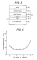
- FIG. 3 there is shown in cross section another example of a semiconductor wafer according to the invention, wherein reference numeral 10 designates an n-type monocrystalline Si substrate on which a plurality of intermediate layers 30 are formed, so as to accommodate a lattice mismatch between the Si substrate 10 and an epitaxial GaAs layer 50 formed on the intermediate layers 30.
- This Example 2 is different from Example 1 in that the four intermediate layers 30 are used in Example 2, in place of the single intermediate GaP layer 30 used in Example 1.
- the intermediate layers 30 of Example 2 consist of: a first intermediate layer in the form of an aluminum phosphide (AIP) layer 31 which is easily epitaxially grown on the Si substrate 10, with a high degree of adherence thereto; a second intermediate layer in the form of an aluminum gallium phosphide (Al 0.5 Ga 0.5 P) layer 32 formed on the first intermediate AIP layer 31; a third intermediate layer in the form of ten superlattice layers 33 of gallium phosphide (GaP) and gallium arsenide-phosphide (GaAs o . s P o . s ), formed on the second intermediate Ai o .
- AIP aluminum phosphide
- GaP gallium phosphide
- GaAs o . s P o . s gallium arsenide-phosphide
- Ga o .gP layer 32 s Ga o .gP layer 32; and a fourth intermediate layer in the form of ten superlattice layers 34 of gallium arsenide (GaAs o . 5 P o . 5 ) and gallium arsenide (GaAs), formed on the third intermediate GaP/GaAs 0.5 P 0.5 superlattice layer 33.
- the Si substrate 10 is 300 micrometers thick, and the epitaxial GaP layer 50 is 2 micrometers thick.
- the four intermediate layers 30 have a total thickness of 0.42 micrometer.
- Each of the first and second intermediate layers 31, 32 is 10 nm (100 Angstroms) thick.
- Example 1 a metalorganic chemical vapor deposition process (MOCVD) was employed to form the intermediate layers 30 and the GaAs layer 50.
- MOCVD metalorganic chemical vapor deposition process
- TMAi - AI(CH 3 ) 3 trimethylaluminum
- the temperature during the epitaxial growth of the first through fourth intermediate layers 31-34 was 830°C
- the temperature during the epitaxial growth of the GaAs layer 50 was 730°C.
- the other conditions were the same as in Example 1.
- the photoluminescence full-width at half maximum (meV) was measured for each wafer prepared.
- the measurements of the individual wafers are shown in Fig. 4.
- the meV value is lower with the substrate off angle within a range between 0.5° to 5°, than that with the substrate off angle of 0°.
- Comparatively good results were obtained with the Si substrates 10 having an off angle within a range from 1° to 4°, and the best results were obtained with the Si substrate 10 with an off angle in the neighborhood of 2°.
- Example 4 the first and second intermediate layers 31 and 32 of the wafer of Fig. 3 were replaced by a single GaP layer having a thickness of 0.5 micrometer. Photoluminescence tests showed similar results, i.e., improved crystallinity of the GaAs layer 50 on the wafers whose Si substrates 50 have an off angle between 0.5° and 5°.
- a wafer prepared according to Example 5 is depicted in Fig. 5.
- the wafer includes a plurality of intermediate layers 30 to accommodate a lattice mismatch between an n-type monocrystalline (100)-oriented Si substrate 10 (with an off angle of 0°) and an epitaxial GaAs layer 50.
- the intermediate layers 30 consist of: a first intermediate layer in the form of a GaP layer formed on the Si substrate 10; a second intermediate layer in the form of ten superlattice layers 32 of gallium phosphide (GaP) and gallium arsenide-phosphide (GaAs o . 5 P O .
- GaP layer 31 formed on the GaP layer 31; and a third intermediate layer in the form of ten superlattice layers 33 of gallium arsenide (GaAs 0.5 P 0.5 ) and gallium arsenide (GaAs), formed on the second intermediate GaP/GaAs o . s P o . s superlattice layer 32.
- the Si substrate 10 is 300 micrometers thick, and the epitaxial GaP layer 50 is 2 micrometers thick.
- the three intermediate layers 30 (31, 32, 33) have a total thickness of 0.9 micrometer.
- the first intermediate layer 31 is 0.5 micrometer thick.
- Each of the ten second intermediate GaP/GaAs o . s P o . s superlattice layers 32, and each of the ten third intermediate GaAs 0.5 P 0.5 /GaAs superlattice layers 33 have a thickness of 20 nm (200 Angstroms).
- the intermediate layers 30 and the epitaxial GaAs layers were formed continuously by epitaxy on the Si substrate 10, in a metalorganic chemical vapor deposition process (MOCVD), within a horizontal induction-heating furnace under the atmospheric pressure.
- MOCVD metalorganic chemical vapor deposition process
- materials for the vapor deposition trimethylgallium (TMGa, Ga(Ch 3 ) 3 ), arsine (AsH 3 ) and phosphine (PH 3 ) were employed.
- TMGa, Ga(Ch 3 ) 3 trimethylgallium
- arsine AsH 3
- phosphine phosphine
- the Si substrate 10 Prior to starting the epitaxy, the Si substrate 10 was first annealed at 950°C with a flow of PH 3 at 100 cc/min. Thereafter, the Si substrate 10 was maintained at 900°C to permit an epitaxial growth of GaP into the first intermediate GaP layer 31, and then at 830°C to allow epitaxial growth of the second and third intermediate superlattice layers 32, 33. Subsequently, the epitaxial growth temperature was lowered down to 650°C, to grow the GaAs layer 50 on the GaAs 0.5 P 0 . 5 /GaAs superlattice layer 33.
- the annealing temperature of the Si substrate 10 may be selected within a range from 600°C to 1100°C, and the annealing period during which the Si substrate 10 is exposed to PH 3 may be selected within a range from 1 to 60 minutes.
- the semiconductor wafer of Fig. 5 (Sample No. 1) was prepared, and its photoluminescence characteristic was compared with those of Comparative Samples Nos. 2-4.
- the measured photoluminescence full-width at half maximum (meV) at 150°K are indicated in the following table.
- Comparative Sample No. 3 using a single intermediate layer of Ge had the largest measurement of 62 meV, and that the second largest measurement (52 meV) was obtained on Comparative Sample No. 2 which uses GaP/GaAs 0.5 P 0.5 superlattice layers and GaAs 0.5 P 0.5 / GaAs superlattice layers.
- Sample No. 1 of the present Example 5 had a value of 45 meV. This value is considered to indicate a relatively high degree of crystallinity of the GaAs layer 50 of Sample No. 1, in view of the fact that Comparative Sample No. 4 which uses a GaAs substrate for an epitaxial GaAs layer had a value of 33 meV.
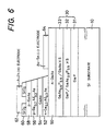
- reference numeral 10 designates an n-type monocrystalline Si substrate having a major surface which is inclined at 2° with respect to the (100) orientation.
- Reference numeral 30 generally indicates a plurality of intermediate layers, while reference numeral 50 indicates an n-type epitaxially grown GaAs layer.
- n-Ga 0.7 Al 0.3 As cladding layer 52 On the epitaxial GaAs layer 50, the following layers are superposed on each other in the order of description: n-Ga 0.7 Al 0.3 As cladding layer 52; i-GaAs active layer 54; p-Ga 0.7 Al 0.3 As cladding layer 56; P-GaAs cap layer 58; SiO 2 insulating layer 60; and Au-Zn electrode 62 (anode).
- An Au-Sn electrode 64 cathode is also formed on the epitaxial n-GaAs layer 50.
- the thicknesses of the layers 10, 30, 50, 52, 54, 56 and 58 are as follows:
- the intermediate layers 30 consist of: a first intermediate layer in the form of a single GaP layer 31 formed on the Si substrate 10; a second intermediate layer in the form of five Gap/GaAs o . s P o . s superlattice layers 32 formed on the GaP layer 31; and a third intermediate layer in the form of five GaAs 0.5 P 0.5 /GaAs superlattice layers 33 formed on the second intermediate layer 32.
- the first intermediate GaP layer 31 has a thickness of 50 nm (500 Angstroms)
- each superlattice layer of the second and third intermediate layers 32, 33 has a thickness of 20 nm (200 Angstroms).
- the layers 30, 50, 52, 54, 56 and 58 were formed continuously on each other by epitaxy on the Si substrate 10, in a metalorganic chemical vapor deposition process (MOCVD), in a horizontal induction-heating furnace under the atmospheric pressure.
- MOCVD metalorganic chemical vapor deposition process
- materials for the vapor deposition trimethylgallium (TMGa, Ga(Ch 3 ) 3 ), trimethylaluminum (TMAI - AI(CH 3 ) 3 ), arsine (AsH 3 ) and phosphine (PH 3 ) were employed.
- TMGa, Ga(Ch 3 ) 3 trimethylaluminum
- TMAI - AI(CH 3 ) 3 trimethylaluminum
- arsine AsH 3
- phosphine phosphine
- p-type and n-type dopants dietylzinc (DEZn) and hydrogen selenide (H 3 Se) were used.
- the flow rates of these gases were controlled accurately by a flow control device so as to achieve a suitable rate of epitaxial growth of crystals. No pre-cracking of the Group V elements was effected.
- the Si substrate 10 Prior to starting the epitaxy, the Si substrate 10 was first annealed at 950°C with a flow of PH 3 at 100 cc/min., to remove the oxide layer from its surface. Thereafter, the Si substrate 10 was maintained at 900°C to permit an epitaxial growth of a GaP crystal into the first intermediate GaP layer 31, and then at 700°C to allow epitaxial growth of the second and third intermediate superlattice layers 32, 33.
- the epitaxial growth temperature of 700° was further maintained to grow the n-GaAs layer, n-Ga 0.7 Al 0.3 As cladding layer 52, GaAs active layer 54, p-Ga 0.7 Al 0.3 As cladding layer 56 and p-GaAs cap layer 58.
- the surface of the p-GaAs cap layer 58 was coated with a photoresist or light-sensitive coating. A selected area of the applied photoresist coating was covered with a mask, and the non-covered area of the photoresist coating was exposed to light, to provide a mask for a subsequent etching process.
- the portions of the layers 52, 54, 56, 58 corresponding to the exposed area of the photoresist were removed in the etching process, whereby a portion of the surface of the n-GaAs layer 50 was exposed, as shown in Fig. 6.
- Si0 2 was applied to the surface of the p-GaAs cap layer 58, to form the Si0 2 insulating layer 60.
- a recess was formed in the insulating layer 60 in a known photolithographic manner, and the Au-Zn electrode 62 (anode) was formed by vapor deposition on the insulating layer 60.
- the Au-Zn electrode 64 cathode was formed by vapor deposition and diffusion on the exposed surface of the n-GaAs layer.
- the thus prepared multilayered structure was cut into a plurality of laser diodes, such that each diode had a laser emitting face.
- the laser diodes were activated to produce a lasing action.
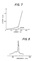
- the input-output characteristic curve is shown in Fig. 7.
- the threshold value of current was 460 mA.
- the spectrum of the emitted light is given in Fig. 8.
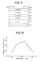
- reference numeral 13 indicates an n-type monocrystalline Si substrate having a major surface which is inclined at 2° with respect to (100).
- Si substrate 13 On this Si substrate 13, there are formed an intermediate n + Gap layer 34, an epitaxial n + GaAs layer 70, an epitaxial n- GaAs layer 71, and an epitaxial p-GaAs layer 72.
- a Au-Zn electrode 73 and a Au-Sn electrode 74 are formed on the top surface of the p-GaAs layer 72 and the bottom surface of the Si substrate 13, respectively.
- the layers 70, 71 and 72 constitute a PIN diode.
- the Si substrate 13 which has an initial thickness of 300 micrometers, was ground to 50 micrometers after the layers 34, 70-72 had been formed thereon by epitaxy. Thicknesses of the epitaxially grown layers 34, 71, 72 and 73 are 1 micrometer, 0.5 micrometer, 2.5 micrometers and 0.5 micrometer, respectively. These layers were formed in an MOCVD process as practiced in the preceding Examples.
- the intermediate layer 34 was grown at 900°C, and the layers 71-73 were grown at 650°C. After these layers were formed by epitaxy, the electrodes 73, 74 were vapor deposited, and the prepared multilayered structure was cut into a plurality of photodiodes, such that each photodiode had a light receiving face.
- the quantum efficiency (emitted energy/incident energy) of the thus produced photodiodes, in relation to the wavelength, is shown in Fig. 10.
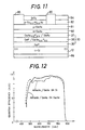
- reference numeral 12 designates an n-type monocrystalline Si substrate having a major surface which is inclined at 2° to (100).
- Si substrate 12 On this Si substrate 12, there are epitaxially formed the following epitaxial layers: a first intermediate GaP layer 35; a second intermediate layer in the form of GaP/ GaAs O . 5 P O . 5 superlattice layers 36; a third intermediate layer in the form of GaAs o .gP o .
- Reference numeral 84 designates a non-reflection Si0 2 coating
- numerals 85 and 86 indicate Au-Zn and AI electrodes, respectively.
- the Si substrate 12 which has an initial thickness of 300 micrometers, was ground to 50 micrometers after the intermediate layers 35-37 and the layers 80-82, 84 had been epitaxially grown thereon.
- the first intermediate GaP layer 35 is 50 nm (500 Angstroms) thick.
- the thicknesses of the layers 80, 81, 82 and 84 are 0.5 micrometer, 0.5 micrometer, 0.1 micrometer and 80 nanometers, respectively.
- These epitaxial layers 35 ⁇ 37, 80 ⁇ 82 were formed in a metalorganic chemical vapor deposition process (MOCVD) as in the preceding Examples.
- MOCVD metalorganic chemical vapor deposition process
- the growth temperature was 900°C for the intermediate layer 35, and 650°C for the layers 80-82.
- Si0 2 was applied by sputtering to form the non-reflection coating 84 on the layer 82.
- recesses were formed in the selected areas of the coating 84 and the layer 82, in order to accommodate the Au-Zn electrodes 85 which were formed by vapor deposition.
- the Si substrate 12 was ground to 50 micrometers as previously mentioned.
- the AI electrode 86 was subsequently formed by vapor deposition.
- the thus prepared solar cell using the silicion substrate 12 exhibited very excellent spectral sensitivity as shown in solid line in Fig. 12. Dashed line in the same figure represents a spectral sensitivity curve of a conventional solar cell using a GaAs substrate.
- the spectral sensitivity of the present Example 8 using the Si substrate 12 is comparable to that of the conventional cell using the GaAs substrate.
- the gallium arsenide wafers employed for the semiconductor devices of Examples 6-8 use a silicon substrate whose major surface is inclined at 2° to (100), the off angle of the substrates of these examples may be zero. In this case, too, the GaAs layers are given a satisfactory level of crystallinity. Further, the semiconductor devices of Examples 6-8 may use the semiconductor wafers of Examples 2 and 3.
- the GaAs light emitting layer 54 of Example 6 may be replaced by a AIGaP layer.
Claims (9)
einer Vielzahl von kristallinen Halbleiterschichten, die als Grundelemente GaAs enthalten und die auf der epitaxialen GaAs-Schicht durch Epitaxie wachsen gelassen und aufeinandergeschichtet worden sind, wobei die kristallinen Halbleiterschichten eine lichtemittierende Schicht enthalten.
wenigstens einem Halbleiterbauelement, das auf der epitaxialen GaAs-Schicht gebildet ist.
Applications Claiming Priority (8)
| Application Number | Priority Date | Filing Date | Title |
|---|---|---|---|
| JP60195629A JPS6258615A (ja) | 1985-09-03 | 1985-09-03 | 砒素化ガリウム系化合物半導体装置 |
| JP195628/85 | 1985-09-03 | ||
| JP60195628A JPS6258614A (ja) | 1985-09-03 | 1985-09-03 | 砒素化ガリウムエピタキシヤルウエハ及びその製造方法 |
| JP195630/85 | 1985-09-03 | ||
| JP19563085A JPS6258616A (ja) | 1985-09-03 | 1985-09-03 | 砒素化ガリウムエピタキシヤルウエハ及びその製造方法 |
| JP195629/85 | 1985-09-03 | ||
| JP195435/85 | 1985-09-04 | ||
| JP60195435A JPS6258690A (ja) | 1985-09-04 | 1985-09-04 | 砒素化ガリウム系半導体発光素子 |
Publications (3)
| Publication Number | Publication Date |
|---|---|
| EP0214610A2 EP0214610A2 (de) | 1987-03-18 |
| EP0214610A3 EP0214610A3 (en) | 1987-12-02 |
| EP0214610B1 true EP0214610B1 (de) | 1990-12-05 |
Family
ID=27475763
Family Applications (1)
| Application Number | Title | Priority Date | Filing Date |
|---|---|---|---|
| EP19860112178 Expired - Lifetime EP0214610B1 (de) | 1985-09-03 | 1986-09-03 | Epitaktische Gallium-Arsenid-Halbleiterscheibe und Verfahren zu ihrer Herstellung |
Country Status (4)
| Country | Link |
|---|---|
| US (2) | US4928154A (de) |
| EP (1) | EP0214610B1 (de) |
| CA (1) | CA1292550C (de) |
| DE (1) | DE3676019D1 (de) |
Families Citing this family (116)
| Publication number | Priority date | Publication date | Assignee | Title |
|---|---|---|---|---|
| JPS6288318A (ja) * | 1985-10-14 | 1987-04-22 | Sharp Corp | 半導体装置の製造方法 |
| JPS63226918A (ja) * | 1987-03-16 | 1988-09-21 | Shin Etsu Handotai Co Ltd | 燐化砒化ガリウム混晶エピタキシヤルウエ−ハ |
| US5130269A (en) * | 1988-04-27 | 1992-07-14 | Fujitsu Limited | Hetero-epitaxially grown compound semiconductor substrate and a method of growing the same |
| JPH0760791B2 (ja) * | 1988-11-04 | 1995-06-28 | シャープ株式会社 | 化合物半導体基板 |
| JPH02235327A (ja) * | 1989-03-08 | 1990-09-18 | Fujitsu Ltd | 半導体成長装置および半導体成長方法 |
| JP3114809B2 (ja) * | 1989-05-31 | 2000-12-04 | 富士通株式会社 | 半導体装置 |
| US5164359A (en) * | 1990-04-20 | 1992-11-17 | Eaton Corporation | Monolithic integrated circuit having compound semiconductor layer epitaxially grown on ceramic substrate |
| US5281834A (en) * | 1990-08-31 | 1994-01-25 | Motorola, Inc. | Non-silicon and silicon bonded structure and method of manufacture |
| US5723871A (en) * | 1991-05-02 | 1998-03-03 | Daido Tokushuko Kabushiki Kaisha | Process of emitting highly spin-polarized electron beam and semiconductor device therefor |
| US5315127A (en) * | 1991-05-02 | 1994-05-24 | Daido Tokushuko Kabushiki Kaisha | Semiconductor device for emitting highly spin-polarized electron beam |
| US5448084A (en) * | 1991-05-24 | 1995-09-05 | Raytheon Company | Field effect transistors on spinel substrates |
| CA2062134C (en) * | 1991-05-31 | 1997-03-25 | Ibm | Low Defect Densiry/Arbitrary Lattice Constant Heteroepitaxial Layers |
| US5208182A (en) * | 1991-11-12 | 1993-05-04 | Kopin Corporation | Dislocation density reduction in gallium arsenide on silicon heterostructures |
| GB2263814B (en) * | 1992-01-17 | 1996-01-10 | Northern Telecom Ltd | Semiconductor mixed crystal quantum well device manufacture |
| FR2691839B1 (fr) * | 1992-05-27 | 1994-08-05 | Schlumberger Ind Sa | Capteur a effet hall. |
| US5747862A (en) * | 1992-09-25 | 1998-05-05 | Katsumi Kishino | Spin-polarized electron emitter having semiconductor opto-electronic layer with split valence band and reflecting mirror |
| JP2576766B2 (ja) * | 1993-07-08 | 1997-01-29 | 日本電気株式会社 | 半導体基板の製造方法 |
| US5536948A (en) * | 1994-08-23 | 1996-07-16 | Grumman Aerospace Corporation | Infrared detector element substrate with superlattice layers |
| US5456206A (en) * | 1994-12-07 | 1995-10-10 | Electronics And Telecommunications Research Institute | Method for two-dimensional epitaxial growth of III-V compound semiconductors |
| US5833749A (en) * | 1995-01-19 | 1998-11-10 | Nippon Steel Corporation | Compound semiconductor substrate and process of producing same |
| JP3268731B2 (ja) * | 1996-10-09 | 2002-03-25 | 沖電気工業株式会社 | 光電変換素子 |
| US6423990B1 (en) * | 1997-09-29 | 2002-07-23 | National Scientific Corporation | Vertical heterojunction bipolar transistor |
| US5912481A (en) * | 1997-09-29 | 1999-06-15 | National Scientific Corp. | Heterojunction bipolar transistor having wide bandgap, low interdiffusion base-emitter junction |
| JP3420087B2 (ja) * | 1997-11-28 | 2003-06-23 | Necエレクトロニクス株式会社 | 半導体発光素子 |
| US6563661B2 (en) | 2000-02-08 | 2003-05-13 | Seagate Technology Llc | Drive-level bearing friction measurement method |
| US6392257B1 (en) | 2000-02-10 | 2002-05-21 | Motorola Inc. | Semiconductor structure, semiconductor device, communicating device, integrated circuit, and process for fabricating the same |
| US6693033B2 (en) | 2000-02-10 | 2004-02-17 | Motorola, Inc. | Method of removing an amorphous oxide from a monocrystalline surface |
| AU2001257346A1 (en) | 2000-05-31 | 2001-12-11 | Motorola, Inc. | Semiconductor device and method for manufacturing the same |
| US6427066B1 (en) | 2000-06-30 | 2002-07-30 | Motorola, Inc. | Apparatus and method for effecting communications among a plurality of remote stations |
| AU2001274913A1 (en) * | 2000-06-30 | 2002-01-14 | Motorola, Inc. | Thin compound semiconductor structure |
| US6477285B1 (en) | 2000-06-30 | 2002-11-05 | Motorola, Inc. | Integrated circuits with optical signal propagation |
| US6501973B1 (en) | 2000-06-30 | 2002-12-31 | Motorola, Inc. | Apparatus and method for measuring selected physical condition of an animate subject |
| AU2001264987A1 (en) * | 2000-06-30 | 2002-01-14 | Motorola, Inc., A Corporation Of The State Of Delware | Hybrid semiconductor structure and device |
| US6410941B1 (en) | 2000-06-30 | 2002-06-25 | Motorola, Inc. | Reconfigurable systems using hybrid integrated circuits with optical ports |
| WO2002009187A2 (en) | 2000-07-24 | 2002-01-31 | Motorola, Inc. | Heterojunction tunneling diodes and process for fabricating same |
| US6555946B1 (en) | 2000-07-24 | 2003-04-29 | Motorola, Inc. | Acoustic wave device and process for forming the same |
| US6638838B1 (en) * | 2000-10-02 | 2003-10-28 | Motorola, Inc. | Semiconductor structure including a partially annealed layer and method of forming the same |
| US6583034B2 (en) | 2000-11-22 | 2003-06-24 | Motorola, Inc. | Semiconductor structure including a compliant substrate having a graded monocrystalline layer and methods for fabricating the structure and semiconductor devices including the structure |
| US6563118B2 (en) | 2000-12-08 | 2003-05-13 | Motorola, Inc. | Pyroelectric device on a monocrystalline semiconductor substrate and process for fabricating same |
| US20020096683A1 (en) | 2001-01-19 | 2002-07-25 | Motorola, Inc. | Structure and method for fabricating GaN devices utilizing the formation of a compliant substrate |
| US6673646B2 (en) | 2001-02-28 | 2004-01-06 | Motorola, Inc. | Growth of compound semiconductor structures on patterned oxide films and process for fabricating same |
| US7046719B2 (en) | 2001-03-08 | 2006-05-16 | Motorola, Inc. | Soft handoff between cellular systems employing different encoding rates |
| WO2002082551A1 (en) | 2001-04-02 | 2002-10-17 | Motorola, Inc. | A semiconductor structure exhibiting reduced leakage current |
| US20020195599A1 (en) * | 2001-06-20 | 2002-12-26 | Motorola, Inc. | Low-defect semiconductor structure, device including the structure and method for fabricating structure and device |
| US6709989B2 (en) | 2001-06-21 | 2004-03-23 | Motorola, Inc. | Method for fabricating a semiconductor structure including a metal oxide interface with silicon |
| US6992321B2 (en) | 2001-07-13 | 2006-01-31 | Motorola, Inc. | Structure and method for fabricating semiconductor structures and devices utilizing piezoelectric materials |
| US6646293B2 (en) | 2001-07-18 | 2003-11-11 | Motorola, Inc. | Structure for fabricating high electron mobility transistors utilizing the formation of complaint substrates |
| US7019332B2 (en) | 2001-07-20 | 2006-03-28 | Freescale Semiconductor, Inc. | Fabrication of a wavelength locker within a semiconductor structure |
| US6693298B2 (en) | 2001-07-20 | 2004-02-17 | Motorola, Inc. | Structure and method for fabricating epitaxial semiconductor on insulator (SOI) structures and devices utilizing the formation of a compliant substrate for materials used to form same |
| US6472694B1 (en) | 2001-07-23 | 2002-10-29 | Motorola, Inc. | Microprocessor structure having a compound semiconductor layer |
| US6855992B2 (en) | 2001-07-24 | 2005-02-15 | Motorola Inc. | Structure and method for fabricating configurable transistor devices utilizing the formation of a compliant substrate for materials used to form the same |
| US6594414B2 (en) | 2001-07-25 | 2003-07-15 | Motorola, Inc. | Structure and method of fabrication for an optical switch |
| US6667196B2 (en) | 2001-07-25 | 2003-12-23 | Motorola, Inc. | Method for real-time monitoring and controlling perovskite oxide film growth and semiconductor structure formed using the method |
| US6585424B2 (en) | 2001-07-25 | 2003-07-01 | Motorola, Inc. | Structure and method for fabricating an electro-rheological lens |
| US6462360B1 (en) | 2001-08-06 | 2002-10-08 | Motorola, Inc. | Integrated gallium arsenide communications systems |
| US6639249B2 (en) | 2001-08-06 | 2003-10-28 | Motorola, Inc. | Structure and method for fabrication for a solid-state lighting device |
| US6589856B2 (en) | 2001-08-06 | 2003-07-08 | Motorola, Inc. | Method and apparatus for controlling anti-phase domains in semiconductor structures and devices |
| US20030034491A1 (en) | 2001-08-14 | 2003-02-20 | Motorola, Inc. | Structure and method for fabricating semiconductor structures and devices for detecting an object |
| US6673667B2 (en) | 2001-08-15 | 2004-01-06 | Motorola, Inc. | Method for manufacturing a substantially integral monolithic apparatus including a plurality of semiconductor materials |
| US6730987B2 (en) * | 2001-09-10 | 2004-05-04 | Showa Denko K.K. | Compound semiconductor device, production method thereof, light-emitting device and transistor |
| US20030071327A1 (en) | 2001-10-17 | 2003-04-17 | Motorola, Inc. | Method and apparatus utilizing monocrystalline insulator |
| US7329554B2 (en) * | 2001-11-08 | 2008-02-12 | Midwest Research Institute | Reactive codoping of GaAlInP compound semiconductors |
| US7309832B2 (en) * | 2001-12-14 | 2007-12-18 | Midwest Research Institute | Multi-junction solar cell device |
| WO2003052836A1 (en) * | 2001-12-14 | 2003-06-26 | Midwest Research Institute | Multi-junction solar cell device |
| US6916717B2 (en) | 2002-05-03 | 2005-07-12 | Motorola, Inc. | Method for growing a monocrystalline oxide layer and for fabricating a semiconductor device on a monocrystalline substrate |
| WO2003100868A1 (en) * | 2002-05-21 | 2003-12-04 | Midwest Research Institute | Low-bandgap, monolithic, multi-bandgap, optoelectronic devices |
| US20060162768A1 (en) * | 2002-05-21 | 2006-07-27 | Wanlass Mark W | Low bandgap, monolithic, multi-bandgap, optoelectronic devices |
| US8173891B2 (en) * | 2002-05-21 | 2012-05-08 | Alliance For Sustainable Energy, Llc | Monolithic, multi-bandgap, tandem, ultra-thin, strain-counterbalanced, photovoltaic energy converters with optimal subcell bandgaps |
| US7169619B2 (en) | 2002-11-19 | 2007-01-30 | Freescale Semiconductor, Inc. | Method for fabricating semiconductor structures on vicinal substrates using a low temperature, low pressure, alkaline earth metal-rich process |
| US6885065B2 (en) | 2002-11-20 | 2005-04-26 | Freescale Semiconductor, Inc. | Ferromagnetic semiconductor structure and method for forming the same |
| WO2004049459A1 (en) * | 2002-11-25 | 2004-06-10 | The University Of Toledo | Integrated photoelectrochemical cell and system having a solid polymer electrolyte |
| WO2004050961A1 (en) * | 2002-11-27 | 2004-06-17 | University Of Toledo, The | Integrated photoelectrochemical cell and system having a liquid electrolyte |
| US6965128B2 (en) | 2003-02-03 | 2005-11-15 | Freescale Semiconductor, Inc. | Structure and method for fabricating semiconductor microresonator devices |
| US7020374B2 (en) | 2003-02-03 | 2006-03-28 | Freescale Semiconductor, Inc. | Optical waveguide structure and method for fabricating the same |
| US6786390B2 (en) * | 2003-02-04 | 2004-09-07 | United Epitaxy Company Ltd. | LED stack manufacturing method and its structure thereof |
| JP2004265945A (ja) * | 2003-02-21 | 2004-09-24 | Sumitomo Chem Co Ltd | 半導体エピタキシャル結晶ウエハの品質判定方法並びにこれを用いたウエハ製造方法 |
| US7109465B2 (en) * | 2003-04-04 | 2006-09-19 | Avago Technologies Ecbu Ip (Singapore) Pte., Ltd. | System and method for converting ambient light energy into a digitized electrical output signal for controlling display and keypad illumination on a battery powered system |
| US7667133B2 (en) * | 2003-10-29 | 2010-02-23 | The University Of Toledo | Hybrid window layer for photovoltaic cells |
| US20080223439A1 (en) * | 2004-02-19 | 2008-09-18 | Xunming Deng | Interconnected Photoelectrochemical Cell |
| US20060011129A1 (en) * | 2004-07-14 | 2006-01-19 | Atomic Energy Council - Institute Of Nuclear Energy Research | Method for fabricating a compound semiconductor epitaxial wafer |
| US8772628B2 (en) | 2004-12-30 | 2014-07-08 | Alliance For Sustainable Energy, Llc | High performance, high bandgap, lattice-mismatched, GaInP solar cells |
| WO2006110613A2 (en) * | 2005-04-11 | 2006-10-19 | The University Of Toledo | Integrated photovoltaic-electrolysis cell |
| US8324660B2 (en) | 2005-05-17 | 2012-12-04 | Taiwan Semiconductor Manufacturing Company, Ltd. | Lattice-mismatched semiconductor structures with reduced dislocation defect densities and related methods for device fabrication |
| US9153645B2 (en) | 2005-05-17 | 2015-10-06 | Taiwan Semiconductor Manufacturing Company, Ltd. | Lattice-mismatched semiconductor structures with reduced dislocation defect densities and related methods for device fabrication |
| KR100641063B1 (ko) * | 2005-08-26 | 2006-11-01 | 삼성전자주식회사 | 단결정 구조물 형성 방법 및 이를 이용한 반도체 장치의제조 방법 |
| WO2007112066A2 (en) | 2006-03-24 | 2007-10-04 | Amberwave Systems Corporation | Lattice-mismatched semiconductor structures and related methods for device fabrication |
| US20070252216A1 (en) * | 2006-04-28 | 2007-11-01 | Infineon Technologies Ag | Semiconductor device and a method of manufacturing such a semiconductor device |
| EP2062290B1 (de) | 2006-09-07 | 2019-08-28 | Taiwan Semiconductor Manufacturing Company, Ltd. | Defektreduzierung durch kontrolle des aspektverhältnisses |
| US7541105B2 (en) * | 2006-09-25 | 2009-06-02 | Seagate Technology Llc | Epitaxial ferroelectric and magnetic recording structures including graded lattice matching layers |
| US7875958B2 (en) | 2006-09-27 | 2011-01-25 | Taiwan Semiconductor Manufacturing Company, Ltd. | Quantum tunneling devices and circuits with lattice-mismatched semiconductor structures |
| WO2008051503A2 (en) | 2006-10-19 | 2008-05-02 | Amberwave Systems Corporation | Light-emitter-based devices with lattice-mismatched semiconductor structures |
| US8304805B2 (en) | 2009-01-09 | 2012-11-06 | Taiwan Semiconductor Manufacturing Company, Ltd. | Semiconductor diodes fabricated by aspect ratio trapping with coalesced films |
| WO2008124154A2 (en) | 2007-04-09 | 2008-10-16 | Amberwave Systems Corporation | Photovoltaics on silicon |
| US8237151B2 (en) | 2009-01-09 | 2012-08-07 | Taiwan Semiconductor Manufacturing Company, Ltd. | Diode-based devices and methods for making the same |
| US7825328B2 (en) | 2007-04-09 | 2010-11-02 | Taiwan Semiconductor Manufacturing Company, Ltd. | Nitride-based multi-junction solar cell modules and methods for making the same |
| US8329541B2 (en) | 2007-06-15 | 2012-12-11 | Taiwan Semiconductor Manufacturing Company, Ltd. | InP-based transistor fabrication |
| JP2010538495A (ja) | 2007-09-07 | 2010-12-09 | アンバーウェーブ・システムズ・コーポレーション | 多接合太陽電池 |
| EP2270832B1 (de) * | 2008-03-25 | 2016-02-10 | Japan Science and Technology Agency | Spin-polarisierte elektronenquelle |
| US8183667B2 (en) | 2008-06-03 | 2012-05-22 | Taiwan Semiconductor Manufacturing Co., Ltd. | Epitaxial growth of crystalline material |
| US8274097B2 (en) | 2008-07-01 | 2012-09-25 | Taiwan Semiconductor Manufacturing Company, Ltd. | Reduction of edge effects from aspect ratio trapping |
| US8981427B2 (en) | 2008-07-15 | 2015-03-17 | Taiwan Semiconductor Manufacturing Company, Ltd. | Polishing of small composite semiconductor materials |
| US20100072515A1 (en) | 2008-09-19 | 2010-03-25 | Amberwave Systems Corporation | Fabrication and structures of crystalline material |
| EP2335273A4 (de) | 2008-09-19 | 2012-01-25 | Taiwan Semiconductor Mfg | Formierung von geräten durch übermässiges wachstum der epitaxialschicht |
| US8253211B2 (en) | 2008-09-24 | 2012-08-28 | Taiwan Semiconductor Manufacturing Company, Ltd. | Semiconductor sensor structures with reduced dislocation defect densities |
| US8912428B2 (en) * | 2008-10-22 | 2014-12-16 | Epir Technologies, Inc. | High efficiency multijunction II-VI photovoltaic solar cells |
| US8629446B2 (en) | 2009-04-02 | 2014-01-14 | Taiwan Semiconductor Manufacturing Company, Ltd. | Devices formed from a non-polar plane of a crystalline material and method of making the same |
| US20110073887A1 (en) * | 2009-09-25 | 2011-03-31 | Alliance For Sustainable Energy, Llc | Optoelectronic devices having a direct-band-gap base and an indirect-band-gap emitter |
| JP6080167B2 (ja) * | 2010-10-01 | 2017-02-15 | アプライド マテリアルズ インコーポレイテッドApplied Materials,Incorporated | 薄膜トランジスタ用途に用いられる砒化ガリウムに基づく材料 |
| US9543468B2 (en) | 2010-10-12 | 2017-01-10 | Alliance For Sustainable Energy, Llc | High bandgap III-V alloys for high efficiency optoelectronics |
| DE102011107657A1 (de) | 2011-07-12 | 2013-01-17 | Nasp Iii/V Gmbh | Monolithische integrierte Halbleiterstruktur |
| US9590131B2 (en) | 2013-03-27 | 2017-03-07 | Alliance For Sustainable Energy, Llc | Systems and methods for advanced ultra-high-performance InP solar cells |
| WO2015026371A1 (en) | 2013-08-23 | 2015-02-26 | Intel Corporation | High resistance layer for iii-v channel deposited on group iv substrates for mos transistors |
| KR102903271B1 (ko) * | 2020-12-03 | 2025-12-22 | 삼성전자주식회사 | 광학 소자 및 그 제조 방법 |
| CN114628556A (zh) * | 2022-03-14 | 2022-06-14 | 厦门士兰明镓化合物半导体有限公司 | Led外延结构及其制造方法 |
| CN115938916B (zh) * | 2022-12-16 | 2025-10-14 | 中芯越州集成电路制造(绍兴)有限公司 | 硅基砷化镓外延结构、激光器及制备方法 |
| CN116247145B (zh) * | 2023-03-28 | 2026-04-17 | 厦门士兰明镓化合物半导体有限公司 | Led外延结构及其制备方法 |
Family Cites Families (13)
| Publication number | Priority date | Publication date | Assignee | Title |
|---|---|---|---|---|
| FR2225207B1 (de) * | 1973-04-16 | 1978-04-21 | Ibm | |
| US4120706A (en) * | 1977-09-16 | 1978-10-17 | Harris Corporation | Heteroepitaxial deposition of gap on silicon substrates |
| US4675709A (en) * | 1982-06-21 | 1987-06-23 | Xerox Corporation | Quantized layered structures with adjusted indirect bandgap transitions |
| JPS5973499A (ja) * | 1982-10-15 | 1984-04-25 | Agency Of Ind Science & Technol | 化合物半導体の成長方法 |
| JPS6012724A (ja) * | 1983-07-01 | 1985-01-23 | Agency Of Ind Science & Technol | 化合物半導体の成長方法 |
| US4632712A (en) * | 1983-09-12 | 1986-12-30 | Massachusetts Institute Of Technology | Reducing dislocations in semiconductors utilizing repeated thermal cycling during multistage epitaxial growth |
| US4558336A (en) * | 1984-03-02 | 1985-12-10 | The United States Of America As Represented By The Secretary Of The Army | MBE Growth technique for matching superlattices grown on GaAs substrates |
| JPS6191098A (ja) * | 1984-10-09 | 1986-05-09 | Daido Steel Co Ltd | シリコン基板上における砒素化ガリウム成長結晶体とその結晶成長方法 |
| JPS61145820A (ja) * | 1984-12-20 | 1986-07-03 | Seiko Epson Corp | 半導体薄膜材料 |
| JPS621224A (ja) * | 1985-06-26 | 1987-01-07 | Sharp Corp | 半導体素子構造 |
| US4774205A (en) * | 1986-06-13 | 1988-09-27 | Massachusetts Institute Of Technology | Monolithic integration of silicon and gallium arsenide devices |
| US4835116A (en) * | 1987-11-13 | 1989-05-30 | Kopin Corporation | Annealing method for III-V deposition |
| US4826784A (en) * | 1987-11-13 | 1989-05-02 | Kopin Corporation | Selective OMCVD growth of compound semiconductor materials on silicon substrates |
-
1986
- 1986-09-03 CA CA000517386A patent/CA1292550C/en not_active Expired - Lifetime
- 1986-09-03 DE DE8686112178T patent/DE3676019D1/de not_active Expired - Lifetime
- 1986-09-03 EP EP19860112178 patent/EP0214610B1/de not_active Expired - Lifetime
-
1989
- 1989-03-20 US US07/325,115 patent/US4928154A/en not_active Expired - Fee Related
-
1990
- 1990-02-22 US US07/483,364 patent/US4963508A/en not_active Expired - Fee Related
Also Published As
| Publication number | Publication date |
|---|---|
| US4928154A (en) | 1990-05-22 |
| CA1292550C (en) | 1991-11-26 |
| US4963508A (en) | 1990-10-16 |
| DE3676019D1 (de) | 1991-01-17 |
| EP0214610A2 (de) | 1987-03-18 |
| EP0214610A3 (en) | 1987-12-02 |
Similar Documents
| Publication | Publication Date | Title |
|---|---|---|
| US4928154A (en) | Epitaxial gallium arsenide semiconductor on silicon substrate with gallium phosphide and superlattice intermediate layers | |
| US7071015B2 (en) | Semiconductor light emitting device and method for producing the same | |
| US6372356B1 (en) | Compliant substrates for growing lattice mismatched films | |
| JP2792785B2 (ja) | 半導体デバイスおよびその製造方法 | |
| US5442205A (en) | Semiconductor heterostructure devices with strained semiconductor layers | |
| US6110277A (en) | Process for the fabrication of epitaxial layers of a compound semiconductor on monocrystal silicon and light-emitting diode fabricated therefrom | |
| JP6484076B2 (ja) | 光デバイス | |
| JP2666237B2 (ja) | 3族窒化物半導体発光素子 | |
| US7084421B2 (en) | Light-emitting device using group III nitride group compound semiconductor | |
| US20020050288A1 (en) | Solar cell and process of manufacturing the same | |
| JP2001284736A (ja) | 窒化物系半導体発光素子及び窒化物系半導体基板 | |
| JP3207918B2 (ja) | Iii−v族化合物の多結晶半導体材料を用いた発光素子およびその製造方法 | |
| EP0177903B1 (de) | Halbleiteranordnung mit monokristalliner Schicht aus Ga-As auf einem Substrat aus Silicium und Verfahren zu deren Herstellung | |
| KR100433039B1 (ko) | 에피택셜웨이퍼및그제조방법 | |
| KR100289595B1 (ko) | 3족질화물반도체발광소자 | |
| CA1322040C (en) | Epitaxial gallium arsenide semiconductor wafer and method of producing the same | |
| JP4024965B2 (ja) | エピタキシャルウエハおよび発光ダイオード | |
| US6218681B1 (en) | Gallium arsenide phosphide epitaxial wafer and light emitting diode | |
| JP2005136136A (ja) | 半導体装置の製造方法およびウエーハの製造方法 | |
| JP3236649B2 (ja) | 半導体発光素子 | |
| JPH05235406A (ja) | 半導体発光素子 | |
| JP4987240B2 (ja) | 化合物半導体素子、化合物半導体素子の製造方法、ダイオード素子 | |
| JPH0793452B2 (ja) | タンデムヘテロ光電変換素子の製造方法 | |
| JPH08125223A (ja) | 3族窒化物半導体発光素子及びその製造方法 | |
| CN114242851A (zh) | 一种半导体器件及其制作方法 |
Legal Events
| Date | Code | Title | Description |
|---|---|---|---|
| PUAI | Public reference made under article 153(3) epc to a published international application that has entered the european phase |
Free format text: ORIGINAL CODE: 0009012 |
|
| AK | Designated contracting states |
Kind code of ref document: A2 Designated state(s): DE FR GB NL |
|
| PUAL | Search report despatched |
Free format text: ORIGINAL CODE: 0009013 |
|
| RHK1 | Main classification (correction) |
Ipc: H01L 29/267 |
|
| AK | Designated contracting states |
Kind code of ref document: A3 Designated state(s): DE FR GB NL |
|
| 17P | Request for examination filed |
Effective date: 19880120 |
|
| 17Q | First examination report despatched |
Effective date: 19890807 |
|
| GRAA | (expected) grant |
Free format text: ORIGINAL CODE: 0009210 |
|
| AK | Designated contracting states |
Kind code of ref document: B1 Designated state(s): DE FR GB NL |
|
| REF | Corresponds to: |
Ref document number: 3676019 Country of ref document: DE Date of ref document: 19910117 |
|
| ET | Fr: translation filed | ||
| RIN2 | Information on inventor provided after grant (corrected) |
Free format text: UMENO, MASAYOSHI * SAKAI, SHIRO * YAHAGI, SHINICHIRO |
|
| PLBE | No opposition filed within time limit |
Free format text: ORIGINAL CODE: 0009261 |
|
| STAA | Information on the status of an ep patent application or granted ep patent |
Free format text: STATUS: NO OPPOSITION FILED WITHIN TIME LIMIT |
|
| 26N | No opposition filed | ||
| PGFP | Annual fee paid to national office [announced via postgrant information from national office to epo] |
Ref country code: DE Payment date: 19960906 Year of fee payment: 11 |
|
| PGFP | Annual fee paid to national office [announced via postgrant information from national office to epo] |
Ref country code: GB Payment date: 19970826 Year of fee payment: 12 |
|
| PGFP | Annual fee paid to national office [announced via postgrant information from national office to epo] |
Ref country code: FR Payment date: 19970909 Year of fee payment: 12 |
|
| PGFP | Annual fee paid to national office [announced via postgrant information from national office to epo] |
Ref country code: NL Payment date: 19970929 Year of fee payment: 12 |
|
| PG25 | Lapsed in a contracting state [announced via postgrant information from national office to epo] |
Ref country code: DE Free format text: LAPSE BECAUSE OF NON-PAYMENT OF DUE FEES Effective date: 19980603 |
|
| PG25 | Lapsed in a contracting state [announced via postgrant information from national office to epo] |
Ref country code: GB Free format text: LAPSE BECAUSE OF NON-PAYMENT OF DUE FEES Effective date: 19980903 |
|
| PG25 | Lapsed in a contracting state [announced via postgrant information from national office to epo] |
Ref country code: NL Free format text: LAPSE BECAUSE OF NON-PAYMENT OF DUE FEES Effective date: 19990401 |
|
| GBPC | Gb: european patent ceased through non-payment of renewal fee |
Effective date: 19980903 |
|
| PG25 | Lapsed in a contracting state [announced via postgrant information from national office to epo] |
Ref country code: FR Free format text: LAPSE BECAUSE OF NON-PAYMENT OF DUE FEES Effective date: 19990531 |
|
| NLV4 | Nl: lapsed or anulled due to non-payment of the annual fee |
Effective date: 19990401 |
|
| REG | Reference to a national code |
Ref country code: FR Ref legal event code: ST |