EP0219037A2 - Wellenformverarbeitungsschaltung - Google Patents
Wellenformverarbeitungsschaltung Download PDFInfo
- Publication number
- EP0219037A2 EP0219037A2 EP86113848A EP86113848A EP0219037A2 EP 0219037 A2 EP0219037 A2 EP 0219037A2 EP 86113848 A EP86113848 A EP 86113848A EP 86113848 A EP86113848 A EP 86113848A EP 0219037 A2 EP0219037 A2 EP 0219037A2
- Authority
- EP
- European Patent Office
- Prior art keywords
- signal
- processing circuit
- producing
- control pulse
- wave processing
- Prior art date
- Legal status (The legal status is an assumption and is not a legal conclusion. Google has not performed a legal analysis and makes no representation as to the accuracy of the status listed.)
- Granted
Links
Images


Classifications
-
- G—PHYSICS
- G11—INFORMATION STORAGE
- G11B—INFORMATION STORAGE BASED ON RELATIVE MOVEMENT BETWEEN RECORD CARRIER AND TRANSDUCER
- G11B5/00—Recording by magnetisation or demagnetisation of a record carrier; Reproducing by magnetic means; Record carriers therefor
- G11B5/02—Recording, reproducing, or erasing methods; Read, write or erase circuits therefor
- G11B5/027—Analogue recording
- G11B5/035—Equalising
-
- G—PHYSICS
- G11—INFORMATION STORAGE
- G11B—INFORMATION STORAGE BASED ON RELATIVE MOVEMENT BETWEEN RECORD CARRIER AND TRANSDUCER
- G11B20/00—Signal processing not specific to the method of recording or reproducing; Circuits therefor
- G11B20/10—Digital recording or reproducing
- G11B20/10009—Improvement or modification of read or write signals
Definitions
- the present invention relates to a waveform processing circuit for use, for example, in a reproducing circuit of a photomagnetic disc system.
- the waveform processing circuit will be described in connection with a reproducing circuit of a photomagnetic disc system, as an example.
- a photomagnetic disc recording and reproducing system has a laser beam generator for generating a converged laser beam having a diameter of about 1 micrometer on a disc.
- the disc has a laminated film which shows a photomagnetic effect.
- a relatively strong pulsating laser beam (high level beam) carrying information is impinged on the disc to increase the temperature of the impinged spot on the film.
- the spot on the film where the temperature is increased looses the coercive force so that the spot is mangetized in a certain direction effected by a magnetic field produced around the disc by a magnetic field generator, thereby recording the information.
- the recording of information on the photomagnetic disc is effected on a track aligned with a plurality of sectors (Fig. 2), each sector including a head portion where the address data and other similar data are stored with a high frequency signal in a predetermined format, and a data portion, following the head portion, which is utilized for recording and reproducing the desired data at a high frequency.
- the head portion is impinged with a low level beam to read out (reproduce) the address data and other data stored therein thereby locating the sector on the disc now being impinged with the beam.
- the data portion following the detected head portion is impinged with the high level beam carrying information to record data.
- the head portion is reproduced by the low level beam in the same manner to locate the sector now being impinged with the beam, and then, the data portion following the head portion is impinged with the low level beam to reproduce the recorded data. Accordingly, even in the recording mode, the reproducing operation is carried out for reading the address data in the head portion.
- the reproduced signal Sa from the light detector contains a high frequency component signal (VD-VL) or (VP-VL) carrying wanted data and a low frequency component signal VL caused by the conversion between the optical signal and the electric signal.
- the head portion contains a high frequency signal (VD-VL).
- the data portion contains, under the recording mode, a high frequency signal (VP-VL), and under the reproducing mode, a high frequency signal (VD-VL).
- the signal (VP-VL) is greater than the signal (VD-VL).
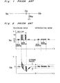
- a high pass filter such as defined by a coupling capacitor Ca and a resistor Ra as shown in Fig. 1 is used.
- the reproduced signal as obtained from the light detector is a current signal, which is converted to a voltage signal by a suitable current-voltage converter.
- the reproduced signal Sa in the voltage form as produced from the current-voltage converter is applied to the high pass filter, and the filter produces a filtered signal Sb which is also shown in Fig. 2.
- the high pass filter When the input signal Sa under the recording mode is applied to the high pass filter, the high pass filter produces an output signal Sb such that the low frequency signal VL is cut off, and the high frequency signal (VD-VL) passes therethrough. But due to the transient phenomena of the high voltage signal VP, the output signal Vo will be deformed greatly. More specifically, as shown in Fig. 2, the output signal Sb gradually decreases after the receipt of the leading edge of the high voltage signal VP and gradually increases after the receipt of the trailing edge of the high voltage signal VP. In this case, since the head portion, as included in the gradual increasing line, may be located outside the dynamic range, the head portion may not be properly read in the subsequent stage, such as the signal detector. Although it is possible to widen the dynamic range to include the head portion therein, the signal becomes poor particularly when the signal is detected at the comparator.
- the present invention has been developed with a view to substantially solving the above described disadvantage and has for its essential object to provide an improved waveform processing circuit by which the high voltage signal VP can be eliminated without deforming the output signal of the high pass filter.
- a waveform processing circuit comprises a switching circuit having first and second inputs and one output.
- the first input is adapted to receive the head portions and the data portions contained in the reproduced signal from the optical head.
- the second input receives a level signal representing the level of the head portion or the level of the signal carrying the head portion.
- the switching circuit is operable to move between a first state in which the first input and the output are connected, and a second state in which the second input and the output are connected.
- a control signal producer is provided for producing a first control pulse indicating the presence of the data portion.
- the first control pulse is applied to the switching circuit for actuating the switching circuit to establish the first state when the first control pulse is present, and to establish the second state when the first control pulse is not present, so that the switching circuit continuously produces the signal having a level within the range of the head portion.
- a photomagnetic disc system which comprises an optical head 50 from which laser beam is produced onto a disc 62, a waveform processing circuit 52, equalizer 54 and signal detector 56 which are connected in series.
- Signal detector 56 is connected to a head portion detector 58 which is in turn connected to a timing pulse generator 60.
- Timing pulses Sl and S2 produced from the timing pulse generator 60 are used in the waveform processing circuit 52. The signals produced from these circuits are described below with reference to Figs. 4 and 5.
- Optical head 50 produces a reproduced voltage signal Sa containing high frequency head portions and high frequency data portions appearing alternately and separated with suitable intervals.
- the head portions and the data portions are carried on a low frequency signal VL.
- the data portions have a relatively high amplitude
- the reproducing mode the data portions have a relatively low amplitude, which is the same as that of the head portions.
- Waveform processing circuit 52 receives the signal Sa and produces a signal Sb which is different between the recording mode and reproducing mode. Under the recording mode, the signal Sb contains only the head portions, and under the reproducing mode, it contains both the head portions and the data portions. In the waveform processing circuit 52, the low frequency signal VL is cut off, so that the head and data portions are now carried on a zero level. According to the present invention no deformation of the output signal Sb is observed which will cause the head portion to be swung out from a predetermined range. The detail of the waveform processing circuit 52 will be described later in connection with Figs. 6-9.
- Equalizer 54 is provided to compensate for an undesired phase frequency response, and produces a signal Sc (Fig. 5) which is substantially the same as the signal Sb, but the waves are more standardized and the slopes are made more steep.
- An example of equalizer 54, defined by a transversal filter, is shown in Fig. 10 which comprises first and second delay circuits DY1 and DY2, buffer amplifiers Bl, B2 and B3 and operational amplifier OP1.
- Other example of the equalizer is disclosed, for example, in Japanese Patent Laid-Open Publication No. 60-107736 published June 13, 1985.
- Signal detector 56 changes the sinusoidal high frequency wave signal contained in the head portion and data portion to a rectangular pulse signal in a binary form.
- signal detector 56 produces signal Sc, as shown in F ig. 5, which is provided to a data demodulator (not shown) and also to head portion detector 58.
- the detail of signal detector 56 will be described later in connection with Figs. 11-14.
- Head portion detector 58 is provided to produce a reference pulse (signal Se) upon detection of the head portion.
- Timing pulse generator 60 generates control pulses S1 and S2 under the recording mode and no control pulse under the reproducing mode.
- Timing pulse generator 60 includes a counter or a delay circuit for counting times Tl, T2, T3 and T4, shown in Fig. 4, after the reference pulse Se is generated so as to prepare control pulses S1 and S2.
- the control pulse S1 has a pulse duration a little greater than the duration of the data portion so as to include the data portion while the control pulse S1 is generated.
- the control pulse S2 has a pulse duration the same as the duration of the data portion and is synchronized with the data portion.
- the control pulses S1 and S2 are used in the waveform processing circuit 52 for extracting the data portion during the recording mode.
- control pulses generated in the second embodiment are different from those of the first embodiment, but are generated in a similar manner described above, and are used for the same purpose.
- the timing pulse generator 60 further produces other pulses to control other circuits (not shown).
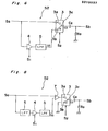
- a first embodiment of the waveform processing circuit 52 which comprises a switching circuit having terminals 3a, 3b and 3c.
- Terminal 3a is connected to the optical head 50 so as to receive the signal Sa directly.
- Terminal 3b is connected to the optical head 50 through a series connection of a sample holding circuit 4 and a low pass filter 5.
- Terminal 3c is connected to a high pass filter defined by capacitor Ca and resistor Ra. The output Sb of the high pass filter is produced as the output of the waveform processing circuit 52.
- Sample holding circuit 4 is controlled by control pulseSl so as to sample the signal Sa in response to the leading edge of the control pulse S1 and holds the sampled signal while the control pulse Sl is present.
- the control pulse S1 is not present, the signal Sa applied to the input of sample holding circuit 4 is transmitted directly to the low pass filter 5.
- Switching circuit 3 is controlled by control pulse S2 such that the terminal 3c is connected to terminal 3b as shown by a real line when the control pulse S2 takes a HIGH level and it is connected to terminal Sa as shown by a dotted line when the control pulse S2 takes a LOW level.
- control pulses Sl and S2 are produced.
- control pulse Sl or S2 is not present.
- the switching circuit 3 is in the position shown by a dotted line.
- the head portion is transmitted through terminals 3a and 3c and through the high pass filter thereby cutting the low frequency level VL.
- the head portion is also transmitted through the sample holding circuit 4 and low pass filter 5, it will not be transmitted through the switching circuit 3.
- the voltage level of signal Sa which is the low frequency level VL, is sampled and held in the circuit 4.
- the switching circuit 3 changes its position to that shown by a real line.
- the sampled low frequency level VL as produced from low pass filter 5 is transmitted through terminals 3b and 3c and through the high pass filter to cut off the low frequency level VL.
- the data portion having a high amplitude is applied to terminal 3a, but it is not transmitted through the switching circuit 3.
- the switching circuit 3 returns back to the position indicated by a dotted line.
- the input signal Sa is again directly transmitted through the switching circuit 3.
- the sample hold circuit 4 releases the sampled signal and permits the signal to pass therethrough. The sampling is effected after each head portion so that the low frequency level VL as sampled by circuit 4 can be renewed after every head portion.
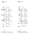
- waveform processing circuit 52 produces a signal Sb as shown by a real line in Fig. 7.
- a second embodiment of the waveform processing circuit 52 is shown, which further comprises a differential amplifier 7.
- a low pass filter 6 is inserted in the input side of the sample and holding circuit 4, but it can be eliminated.
- the non-inverting input of differential amplifier 7 is connected to receive the input signal Sa directly, and inverting input thereof is connected to receive the output of low pass filter 5.
- the output of differential amplifier 7 is connected to terminal 3a. In this embodiment, terminal 3b is connected to ground.
- control pulses S1 and S2 have different pattern.
- the control signal S1 usually takes a HIGH level, but it instantaneously takes a LOW level in the interval between the trailing edge of the head portion and the leading edge of the data portion.
- This pattern of control signal S1 is present both under the recording mode and under the reproducing mode.
- the control signal S2 is the same at that generated in the first embodiment.
- control signals S1 and S2 are produced under the recording mode.
- control signal S1 is HIGH and S2 is LOW.
- sample and holding circuit 4 produces the low frequency level VL which has been sampled in the previous cycle of operation.
- differential amplifier 7 subtracts the low frequency level VL from the header portion, and produces a header portion carried on the zero level to terminal 3a.
- signal S2 is LOW, the switching circuit 3 is in the position shown by a dotted line.
- the head portion is transmitted through terminals 3a and 3c and through the high pass filter.
- the switching circuit 3 changes the position to that shown by a real line.
- the zero volt signal from the ground is transmitted through terminals 3b and 3c and through the high pass filter.
- waveform processing circuit 52 according to the second embodiment produces a signal Sb as shown by a real line in Fig. 9.
- control signal S1 is present, but control signal S2 is not produced, as indicated by dotted lined in Fig. 9.
- the switching circuit 3 is always held in the position so as to connect terminals 3a and 3c as indicated by the dotted line. Therefore, the head portions and the data portions carried on the zero level as produced from differential amplifier 7 are transmitted to the high pass filter.
- the waveform processing circuit of the present invention since the high amplitude data portion will not pass through the high pass filter, there will be no great deformation of the filtered signal as caused by the transient phenomena.
- the waveform processing circuit described herein can be used in the systems other than the photomagnetic disc system. Also, the waveform processing circuit is shown so as to eliminate unwanted transient phenomena caused by the high pass filter, but the circuit may be applied to eliminate unwanted transient phenomena caused by the low pass filter.
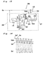
- signal detector 56 which comprises comparator 10 having a non-inverting input 10a and an inverting input Ob.
- the non-inverting input 10a is connected so as to receive the signal Sc produced from equalizer 54, such as shown in Fig. 10, and the inverting input 10b is connected so as to receive a constant voltage Val from a constant voltage generator comprising resistors R4 and R5 connected between a voltage source of Vo and the ground.
- the signal Sc includes the head portion and the data portion defined by a high frequency sinusoidal wave, as shown in Fig. 12.
- Comparator 10 compares the sinusoidal wave Sc with a constant voltage Val and produces a rectangular wave signal Sd of binary form carrying information.
- the constant voltage Val aligns with the center line of the signal Sc
- the rectangular wave signal will be produced with a constant duty ratio such that the duration of one HIGH level period and the duration of one LOW level period will not change.
- the center line of the signal Sc deflects from the constant voltage Val, as shown in Fig. 12, the rectangular wave signal will have different durations of one HIGH level period or one LOW level period, resulting in the error information.
- the signal detector 56 of Fig. 11 is applicable in the cases when the signal Sc is stable, it can not be used when the signal Sc fluctuates.
- an improved signal detector 56 which comprises an envelope detector 26 and a center line detector 27.
- Envelope detector 26 comprises a buffer amplifier 14, diodes Dl and D2, capacitors Cl and C2 arid buffer amplifiers 17 and 20.
- Buffer amplifier 14 receives signal Sc and provides the output thereof to buffer amplifier 17 during the positive half cycle and to buffer amplifier 20 during the negative half cycle.
- Buffer amplifier 17 detects and holds the positive peak value Ve + and buffer amplifier 20 detects and holds the negative peak value Ve-.
- peak values Ve + and Ve- define an envelope of the signal Sc.
- Center line detector 27 comprises resistors R1, R2 and R3 having the same resistance to each other, an opera- ticnal amplifier 24, and a low pass filter 25.
- Operational amplifier 24 produces a voltage signal Vb2 which is an average between Ve+ and Ve-.
- signal Vb2 can be given as follows.
- Vb2 (Ve+ + Ve-) / 2
- the voltage signal Vb2 is applied to low pass filter 25 so as to make the voltage signal smooth.
- the signal Va2 produced from low pass filter 25 closely coincides with the center line of the input signal Sc.
- the input signal Sc is compared with the signal Va2 which closely coincides with the center line of the input signal Sc.
- the signal Sd produced from the comparator 10 shown in Fig. 13 will have a constant duty ratio such that the duration of one HIGH level period and the duration of one LOW level period will not change even when the input signal Sc fluctuates, as shown in Fig. 14.
- signal detector 56 such as shown in Fig. 13
- the data stored in the head portion, as well as in the data portion can be detected with less error, so that the control pulses S1 and S2 as produced relatively to the detection of the head portion can be generated with a high reliability and high accuracy.
Landscapes
- Engineering & Computer Science (AREA)
- Signal Processing (AREA)
- Optical Recording Or Reproduction (AREA)
- Signal Processing For Digital Recording And Reproducing (AREA)
Applications Claiming Priority (4)
| Application Number | Priority Date | Filing Date | Title |
|---|---|---|---|
| JP22459985A JPS6283671A (ja) | 1985-10-08 | 1985-10-08 | 信号検出回路 |
| JP224599/85 | 1985-10-08 | ||
| JP22460085A JPS6282813A (ja) | 1985-10-08 | 1985-10-08 | 波形処理回路 |
| JP224600/85 | 1985-10-08 |
Publications (3)
| Publication Number | Publication Date |
|---|---|
| EP0219037A2 true EP0219037A2 (de) | 1987-04-22 |
| EP0219037A3 EP0219037A3 (en) | 1989-08-30 |
| EP0219037B1 EP0219037B1 (de) | 1993-09-15 |
Family
ID=26526144
Family Applications (1)
| Application Number | Title | Priority Date | Filing Date |
|---|---|---|---|
| EP86113848A Expired - Lifetime EP0219037B1 (de) | 1985-10-08 | 1986-10-07 | Wellenformverarbeitungsschaltung |
Country Status (3)
| Country | Link |
|---|---|
| US (1) | US4785252A (de) |
| EP (1) | EP0219037B1 (de) |
| DE (1) | DE3689023T2 (de) |
Cited By (6)
| Publication number | Priority date | Publication date | Assignee | Title |
|---|---|---|---|---|
| EP0375342A3 (de) * | 1988-12-21 | 1991-07-31 | Matsushita Electric Industrial Co., Ltd. | Datenaufzeichnungs-wiedergabegerät auf einer Aufzeichnungsscheibe |
| EP0357046A3 (de) * | 1988-09-02 | 1991-12-04 | Sharp Kabushiki Kaisha | Signalverarbeitungsanordnung zur Analog-Digital-Wandlung |
| EP0438784A3 (en) * | 1989-12-27 | 1992-07-15 | Sony Corporation | Apparatus for generating clock signals for data reproduction |
| EP0406852A3 (en) * | 1989-07-06 | 1993-08-25 | Hitachi, Ltd. | Automatic gain control method and appartus in optical disk system |
| US5361247A (en) * | 1989-09-12 | 1994-11-01 | Sharp Kabushiki Kaisha | Information recording and reproducing device with reproduction and automatic gain control circuit |
| EP0829962A3 (de) * | 1996-09-12 | 1998-12-30 | Siemens Aktiengesellschaft | Schaltung zur Ermittlung und Speicherung eines Signalmittelwertes |
Families Citing this family (5)
| Publication number | Priority date | Publication date | Assignee | Title |
|---|---|---|---|---|
| US4906874A (en) * | 1988-01-22 | 1990-03-06 | Sharp Kabushiki Kaisha | Analog signal switching device for use in an optical memory |
| JPH04184509A (ja) * | 1990-11-20 | 1992-07-01 | Canon Inc | サンプルホールド回路 |
| US5151662A (en) * | 1991-06-24 | 1992-09-29 | Motorola, Inc. | Circuit and method of signal differentiation |
| CN1882995A (zh) * | 2003-11-18 | 2006-12-20 | 皇家飞利浦电子股份有限公司 | 用于记录介质的复制保护系统 |
| US9979383B2 (en) * | 2016-07-26 | 2018-05-22 | Texas Instruments Incorporated | Delay compensated continuous time comparator |
Family Cites Families (8)
| Publication number | Priority date | Publication date | Assignee | Title |
|---|---|---|---|---|
| US3660821A (en) * | 1970-06-17 | 1972-05-02 | Burroughs Corp | Disc file agc circuit |
| FR2424601A1 (fr) * | 1978-04-25 | 1979-11-23 | Cii Honeywell Bull | Procede d'asservissement du signal de lecture d'un support d'informations et dispositif pour le mettre en oeuvre |
| FR2472304A1 (fr) * | 1979-12-19 | 1981-06-26 | Cii Honeywell Bull | Procede pour commander le gain des circuits amplifiant les signaux delivres par une tete de lecture associee a un support d'informations et dispositif pour le mettre en oeuvre |
| JPS6020962B2 (ja) * | 1980-03-03 | 1985-05-24 | 佐々木農機株式会社 | 四輪トラクタ用フロントデイスクモア |
| US4373141A (en) * | 1981-01-22 | 1983-02-08 | E-Systems, Inc. | Fast updating peak detector circuit |
| US4433255A (en) * | 1981-02-25 | 1984-02-21 | Tokyo Shibaura Denki Kabushiki Kaisha | Signal sampling gate circuit |
| US4538257A (en) * | 1982-12-23 | 1985-08-27 | Xerox Corporation | Adaptively stabilized recording for direct read after write optical memories |
| JPS60219679A (ja) * | 1984-04-13 | 1985-11-02 | Mitsubishi Electric Corp | 情報記録装置 |
-
1986
- 1986-10-07 EP EP86113848A patent/EP0219037B1/de not_active Expired - Lifetime
- 1986-10-07 DE DE86113848T patent/DE3689023T2/de not_active Expired - Fee Related
- 1986-10-08 US US06/916,644 patent/US4785252A/en not_active Expired - Lifetime
Cited By (9)
| Publication number | Priority date | Publication date | Assignee | Title |
|---|---|---|---|---|
| EP0357046A3 (de) * | 1988-09-02 | 1991-12-04 | Sharp Kabushiki Kaisha | Signalverarbeitungsanordnung zur Analog-Digital-Wandlung |
| EP0375342A3 (de) * | 1988-12-21 | 1991-07-31 | Matsushita Electric Industrial Co., Ltd. | Datenaufzeichnungs-wiedergabegerät auf einer Aufzeichnungsscheibe |
| US5166914A (en) * | 1988-12-21 | 1992-11-24 | Matsushita Electric Industrial Co., Ltd. | Data recording/reproducing apparatus with two-dimensional equalizer for crosstalk cancellation |
| EP0406852A3 (en) * | 1989-07-06 | 1993-08-25 | Hitachi, Ltd. | Automatic gain control method and appartus in optical disk system |
| US5361247A (en) * | 1989-09-12 | 1994-11-01 | Sharp Kabushiki Kaisha | Information recording and reproducing device with reproduction and automatic gain control circuit |
| EP0418070B1 (de) * | 1989-09-12 | 1996-11-13 | Sharp Kabushiki Kaisha | Informationsaufzeichnungs- und Wiedergabegerät |
| EP0438784A3 (en) * | 1989-12-27 | 1992-07-15 | Sony Corporation | Apparatus for generating clock signals for data reproduction |
| US5237554A (en) * | 1989-12-27 | 1993-08-17 | Sony Corporation | Apparatus for generating clock signals for data reproduction |
| EP0829962A3 (de) * | 1996-09-12 | 1998-12-30 | Siemens Aktiengesellschaft | Schaltung zur Ermittlung und Speicherung eines Signalmittelwertes |
Also Published As
| Publication number | Publication date |
|---|---|
| EP0219037B1 (de) | 1993-09-15 |
| DE3689023T2 (de) | 1994-02-10 |
| EP0219037A3 (en) | 1989-08-30 |
| US4785252A (en) | 1988-11-15 |
| DE3689023D1 (de) | 1993-10-21 |
Similar Documents
| Publication | Publication Date | Title |
|---|---|---|
| US5101395A (en) | Data detection employing high-speed baseline tracking compensation | |
| US5631891A (en) | Disk reproducing circuit with automatic gain control | |
| US4346411A (en) | Amplitude sensitive three-level detector for derivative read back channel of magnetic storage device | |
| US4785252A (en) | Waveform processing circuit | |
| KR900008413B1 (ko) | 레코드 캐리어로부터 판독된 정보 신호를 구형 신호로 변환시키는 회로장치 | |
| CA1275730C (en) | Reading circuit in an optical disk apparatus | |
| US4706236A (en) | Slice level corrector | |
| EP0312214B1 (de) | Datensignal-Wiedergabegerät | |
| JPH0778428A (ja) | ディスク装置のアクセス方向検知回路 | |
| US4492990A (en) | Noise reduction system | |
| CA1278093C (en) | Method and apparatus for detecting focussing position | |
| JPH0467692B2 (de) | ||
| JPH06223507A (ja) | 信号再生方式 | |
| JPH01159835A (ja) | 光学的情報記録再生装置 | |
| RU1827648C (ru) | Устройство дл воспроизведени и контрол коэффициента глубины амплитудной модул ции сигнала воспроизведени носител магнитной записи | |
| JPH0397118A (ja) | 光ディスク装置 | |
| JPS61940A (ja) | 光学式デイスク再生装置のトラツキング方法 | |
| KR0145008B1 (ko) | 디지탈 데이타 검출회로 | |
| JPH01112569A (ja) | デジタル信号再生装置 | |
| JPH05342584A (ja) | 光ディスク記録再生装置及び記録フォーマット | |
| JPH0258733A (ja) | 光学式情報再生装置 | |
| JPH06162662A (ja) | 信号再生方式 | |
| JPH0664853B2 (ja) | デ−タ識別装置 | |
| JPH01171161A (ja) | 光情報記録再生装置 | |
| JPH0445890B2 (de) |
Legal Events
| Date | Code | Title | Description |
|---|---|---|---|
| PUAI | Public reference made under article 153(3) epc to a published international application that has entered the european phase |
Free format text: ORIGINAL CODE: 0009012 |
|
| 17P | Request for examination filed |
Effective date: 19870106 |
|
| AK | Designated contracting states |
Kind code of ref document: A2 Designated state(s): DE FR GB NL |
|
| PUAL | Search report despatched |
Free format text: ORIGINAL CODE: 0009013 |
|
| AK | Designated contracting states |
Kind code of ref document: A3 Designated state(s): DE FR GB NL |
|
| 17Q | First examination report despatched |
Effective date: 19910910 |
|
| GRAA | (expected) grant |
Free format text: ORIGINAL CODE: 0009210 |
|
| AK | Designated contracting states |
Kind code of ref document: B1 Designated state(s): DE FR GB NL |
|
| REF | Corresponds to: |
Ref document number: 3689023 Country of ref document: DE Date of ref document: 19931021 |
|
| ET | Fr: translation filed | ||
| PLBE | No opposition filed within time limit |
Free format text: ORIGINAL CODE: 0009261 |
|
| STAA | Information on the status of an ep patent application or granted ep patent |
Free format text: STATUS: NO OPPOSITION FILED WITHIN TIME LIMIT |
|
| 26N | No opposition filed | ||
| PGFP | Annual fee paid to national office [announced via postgrant information from national office to epo] |
Ref country code: NL Payment date: 19981031 Year of fee payment: 13 |
|
| PG25 | Lapsed in a contracting state [announced via postgrant information from national office to epo] |
Ref country code: NL Free format text: LAPSE BECAUSE OF NON-PAYMENT OF DUE FEES Effective date: 20000501 |
|
| NLV4 | Nl: lapsed or anulled due to non-payment of the annual fee |
Effective date: 20000501 |
|
| REG | Reference to a national code |
Ref country code: GB Ref legal event code: IF02 |
|
| PGFP | Annual fee paid to national office [announced via postgrant information from national office to epo] |
Ref country code: GB Payment date: 20031001 Year of fee payment: 18 |
|
| PGFP | Annual fee paid to national office [announced via postgrant information from national office to epo] |
Ref country code: FR Payment date: 20031003 Year of fee payment: 18 |
|
| PGFP | Annual fee paid to national office [announced via postgrant information from national office to epo] |
Ref country code: DE Payment date: 20031016 Year of fee payment: 18 |
|
| PG25 | Lapsed in a contracting state [announced via postgrant information from national office to epo] |
Ref country code: GB Free format text: LAPSE BECAUSE OF NON-PAYMENT OF DUE FEES Effective date: 20041007 |
|
| PG25 | Lapsed in a contracting state [announced via postgrant information from national office to epo] |
Ref country code: DE Free format text: LAPSE BECAUSE OF NON-PAYMENT OF DUE FEES Effective date: 20050503 |
|
| GBPC | Gb: european patent ceased through non-payment of renewal fee |
Effective date: 20041007 |
|
| PG25 | Lapsed in a contracting state [announced via postgrant information from national office to epo] |
Ref country code: FR Free format text: LAPSE BECAUSE OF NON-PAYMENT OF DUE FEES Effective date: 20050630 |
|
| REG | Reference to a national code |
Ref country code: FR Ref legal event code: ST |