EP0241028A2 - Masque photographique utilisé pour la fabrication d'un disque d'enregistrement optique, procédé pour la fabrication de ce masque et procédé pour la fabrication du disque optique - Google Patents
Masque photographique utilisé pour la fabrication d'un disque d'enregistrement optique, procédé pour la fabrication de ce masque et procédé pour la fabrication du disque optique Download PDFInfo
- Publication number
- EP0241028A2 EP0241028A2 EP87105243A EP87105243A EP0241028A2 EP 0241028 A2 EP0241028 A2 EP 0241028A2 EP 87105243 A EP87105243 A EP 87105243A EP 87105243 A EP87105243 A EP 87105243A EP 0241028 A2 EP0241028 A2 EP 0241028A2
- Authority
- EP
- European Patent Office
- Prior art keywords
- film
- grooves
- photo
- mask
- laser
- Prior art date
- Legal status (The legal status is an assumption and is not a legal conclusion. Google has not performed a legal analysis and makes no representation as to the accuracy of the status listed.)
- Granted
Links
- 230000003287 optical effect Effects 0.000 title claims abstract description 21
- 238000004519 manufacturing process Methods 0.000 title claims abstract description 19
- 238000000034 method Methods 0.000 title claims description 15
- 239000010408 film Substances 0.000 claims abstract description 55
- 238000007373 indentation Methods 0.000 claims abstract description 36
- 239000000758 substrate Substances 0.000 claims abstract description 25
- 239000010409 thin film Substances 0.000 claims abstract description 15
- 239000012780 transparent material Substances 0.000 claims abstract description 10
- 238000000151 deposition Methods 0.000 claims abstract description 4
- 229920002120 photoresistant polymer Polymers 0.000 claims description 30
- 239000011521 glass Substances 0.000 claims description 12
- 238000005530 etching Methods 0.000 claims description 4
- 229910052804 chromium Inorganic materials 0.000 claims description 3
- 229910052715 tantalum Inorganic materials 0.000 claims description 3
- 229910052759 nickel Inorganic materials 0.000 claims description 2
- 229910052758 niobium Inorganic materials 0.000 claims description 2
- 239000004033 plastic Substances 0.000 claims description 2
- 229920003023 plastic Polymers 0.000 claims description 2
- 229910052719 titanium Inorganic materials 0.000 claims description 2
- 230000001276 controlling effect Effects 0.000 claims 2
- 239000005022 packaging material Substances 0.000 description 5
- CSCPPACGZOOCGX-UHFFFAOYSA-N Acetone Chemical compound CC(C)=O CSCPPACGZOOCGX-UHFFFAOYSA-N 0.000 description 4
- 239000003795 chemical substances by application Substances 0.000 description 3
- XPDWGBQVDMORPB-UHFFFAOYSA-N Fluoroform Chemical compound FC(F)F XPDWGBQVDMORPB-UHFFFAOYSA-N 0.000 description 2
- VYPSYNLAJGMNEJ-UHFFFAOYSA-N Silicium dioxide Chemical compound O=[Si]=O VYPSYNLAJGMNEJ-UHFFFAOYSA-N 0.000 description 2
- 239000007788 liquid Substances 0.000 description 2
- 238000001020 plasma etching Methods 0.000 description 2
- 239000002904 solvent Substances 0.000 description 2
- 238000004544 sputter deposition Methods 0.000 description 2
- 238000001039 wet etching Methods 0.000 description 2
- 229910052681 coesite Inorganic materials 0.000 description 1
- 229910052906 cristobalite Inorganic materials 0.000 description 1
- 230000006870 function Effects 0.000 description 1
- 239000000463 material Substances 0.000 description 1
- 230000007087 memory ability Effects 0.000 description 1
- 238000012986 modification Methods 0.000 description 1
- 230000004048 modification Effects 0.000 description 1
- 229920003229 poly(methyl methacrylate) Polymers 0.000 description 1
- 239000004926 polymethyl methacrylate Substances 0.000 description 1
- 239000000377 silicon dioxide Substances 0.000 description 1
- 235000012239 silicon dioxide Nutrition 0.000 description 1
- 229910052682 stishovite Inorganic materials 0.000 description 1
- 229910052905 tridymite Inorganic materials 0.000 description 1
Images


Classifications
-
- G—PHYSICS
- G11—INFORMATION STORAGE
- G11B—INFORMATION STORAGE BASED ON RELATIVE MOVEMENT BETWEEN RECORD CARRIER AND TRANSDUCER
- G11B7/00—Recording or reproducing by optical means, e.g. recording using a thermal beam of optical radiation by modifying optical properties or the physical structure, reproducing using an optical beam at lower power by sensing optical properties; Record carriers therefor
- G11B7/24—Record carriers characterised by shape, structure or physical properties, or by the selection of the material
- G11B7/26—Apparatus or processes specially adapted for the manufacture of record carriers
- G11B7/261—Preparing a master, e.g. exposing photoresist, electroforming
Definitions
- the present invention relates to a method for manufacturing an optical memory element, such as an optical memory disc, also to a photo-mask used in the disc manufacturing step, and further to a method for making the photo-mask.
- the optical memory discs can be divided into three types: a read-only type which can only reproduce the recorded data; a read/add type which can reproduce the recorded data and also add further data, but can not erase the original or the added data; and a read/write type which can reproduce, erase and record data freely.
- the discs of the read/add type and the read/write type are previously provided with guide tracks 111 for guiding an area to be recorded, and address indications 112 defined by a number of microscopic pits in the form of minute indentations spaced along the spiral or concentric guide tracks for indicating the addresses of the guide tracks.
- address indications 112 defined by a number of microscopic pits in the form of minute indentations spaced along the spiral or concentric guide tracks for indicating the addresses of the guide tracks.
- sector indications are further provided in the form of indentations.
- a prior art method for manufacturing the optical memory disc is disclosed, for example, in Japanese patent laid-open publication No. 60-195751 (corresponding to the above-mentioned U.S. Patent Application Serial No. (not yet given), filed February 24, 1987, Kenji OHTA et al., entitled "Method of Manufacturing Optical Memory Element") assigned to the same assignee as the present application.
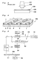
- the prior art method is briefly described hereinbelow in connection with Figs. 2a-2e.
- a glass disc 100 having no track or no indentation is deposited with a photoresist film 101 using a spinner, or the like (Fig 2a).
- a photo-mask M defined by a transparent plate 102 and opaque film 105 having a predetermined pattern and made of, e.g., Cr or Ta is placed on the photoresist film 101 and, thereafter, the photoresist film is exposed by light, such as ultraviolet light UV (Fig. 2b).
- the photoresist is developed in a certain agent so as to remove the photoresist which has been exposed by the light and for the non-exposed areas to remain (Fig. 2c).
- a reactive ion etching is carried out in a chamber filled with CF4 or CHF3 gas, or instead, a wet etching is carried out in a pool filled with HF liquid, so as to form guide tracks 111 and indentations 112 in the glass disc 100 (Fig. 2d).
- the remaining photoresist is removed by solvent such as acetone, or by sputtering in O2 plasma so as to produce a glass disc formed with guide tracks and indentations (Fig. 2e).
- the photo-mask M is formed by the following steps.
- the transparent plate 102 in a shape of disc is deposited with an opaque film 105 and further with a photoresist film 108. Then, while rotating the disc about its center, an Ar laser beam 110 converged by a lens system 109 impinges on the photoresist film 108. A continuous laser beam is produced when tracing the guide tracks and an intermittent laser beam is produced when tracing the places where the indentations are to be formed. Thereafter, the photoresist film is partly removed in a pattern corresponding to the laser beam impingement. Then, by a certain agent, opaque film 105 is etched according to the pattern, and the remaining photoresist is removed, thereby producing the photo-mask M.
- the guide tracks and the indentations will have the same depth.
- the present invention has been developed with a view to substantially solving the above described problem and has for its essential object to provide a method for manufacturing an optical memory disc having a different depth between the guide track and the indentations.
- a photo-mask according to the present invention has a substrate having a disc shape and made of a transparent material, and a film deposited on the substrate and formed with a predetermined pattern of grooves extending spirally or concentrically to the center of the disc shaped substrate so as to leave a thin film at the bottom of the grooves, and a number of microscopic pits in the form of minute indentations with a predetermined spacing aligned along the grooves so as to substantially leave no film at the bottom of the indentations.
- a light which has passed through the thin film at grooves is weakened and a light which has passed through the indentations loses substantially no power, and a light applied elsewhere on the film is cut off.
- a method for making the photo-mask according to the present invention comprises the steps of depositing an opaque film on a substrate having a disc shape and made of a transparent material, impinging a first laser at places where the grooves are to be formed, and impinging a second laser at places where the pits are to be formed.
- the first laser is weaker in power than the second laser.
- the photo-mask PM has a disc shape and comprises a substrate 1 made of a transparent material, such as a glass (SiO2), or plastic (PMMA), and a film 2 made of an opaque material, such as Cr, Ti, Ta, Nb, Ni, etc.
- Film 2 is formed with a predetermined pattern of grooves 4 extending spirally or concentrically to the center of the disc, and a number of microscopic pits in the form of minute indentations 3 with a predetermined spacing aligned along the grooves 4.
- An Ar laser generator 31 produces Ar laser which is split into halves by a half mirror 40.
- One laser beam from half mirror 40 is directed to an attenuator 32 at which the laser beam is weakened to half.
- the laser beam produced from attenuator 32 is about 1/4 of the original laser beam power.
- the laser beam from attenuator 32 is applied to an acoustooptic modulator 33 which controls ON and OFF of the laser beam passing therethrough in accordance with a groove signal obtained from groove signal source 34.
- accoustooptic modulator 33 produces a continuous laser beam for making the grooves 4.
- the other laser beam from half mirror 40 is directed to an acoustooptic modulator 35 which controls ON and OFF of the laser beam passing therethrough in accordance with a pit signal obtained from a pit signal source 36.
- acoustooptic modulator 35 produces an intermittent laser beam for making the pits.
- the continuous and the intermittent laser beams are both directed, at different time periods, to an optical head 37 through suitable mirrors.
- Optical head 37 is positioned above a turntable TT driven by a drive motor 38, and is so arranged to move in the radial direction of the turntable and has a function of focusing the laser beam on an photo-mask PM placed on turntable TT.
- FIGs. 6a-6e a method for manufacturing the optical memory disc according to the present invention is shown.
- a glass disc 5 having no track or no indentation is deposited with a photoresist film 6 using a spinner, or the like (Fig 6a).
- photo-mask PM which has been made in the system shown in Fig. 5, is placed on the photoresist film 6 and, thereafter, the photoresist film is exposed by light, such as ultraviolet light UV (Fig. 6b).
- the ultraviolet light UV passing through the areas 3 loses hardly any power, thus resulting in the full power exposure on the photoresist film 6, but the same passing through the areas 4 loses about 1/2 of its power, thus resulting in the half power exposure on the photoresist film 6.
- the photoresist film 6 is developed in a certain agent so as to remove the photoresist (Fig. 6c) such that the photoresist is removed by its entire thickness where the full power exposure has been effected, and by its 1/n (n is greater than 1 and preferably about 2) thickness where the half power exposure has been effected. No removal of the photoresist is effected at the non-exposed areas.
- an intervene product at the step shown in Fig. 6c may be depicted as shown in Fig. 7.
- a reactive ion etching is carried out in a chamber filled with CF4 or CHF3 gas, or instead, a wet etching is carried out in a pool filled with HF liquid (Fig. 6d). Since there is no photoresist film left in the areas where pits are to be formed, the etching into the glass is effected from the beginning of the step. However, in the areas where grooves are to be formed, there is some photoresist film left, so that the etching into the glass can be effected some time after the beginning of the step. Accordingly, there will be a difference in the depth between the grooves and the pits such that the pits will be deeper than the grooves.
- the remaining photoresist is removed by solvent such as acetone, or by sputtering in O2 plasma so as to produce a glass disc formed with shallow guide tracks and deep indentations (Fig. 6e).
- the width of the tracks and indentations can be selected to any desired size.
- the edges of the grooves and indentations are shown as perpendicular to the bottom face of the disc, but they can be slanted.
- the thickness of the film 2 can be selected to any desired size.
- the thickness of the film 2 is originally about 600-700 ⁇
- the thickness of the film 2 where the guide groove 4 is formed is about 50-150 ⁇ . It is possible for some photoresist layer to remain in the pits 3, such as at the thickness of about 50 ⁇ .
Landscapes
- Engineering & Computer Science (AREA)
- Manufacturing & Machinery (AREA)
- Manufacturing Optical Record Carriers (AREA)
Applications Claiming Priority (2)
| Application Number | Priority Date | Filing Date | Title |
|---|---|---|---|
| JP84448/86 | 1986-04-11 | ||
| JP61084448A JPS62241149A (ja) | 1986-04-11 | 1986-04-11 | 光メモリ素子用フォトマスク及びその製造方法 |
Publications (3)
| Publication Number | Publication Date |
|---|---|
| EP0241028A2 true EP0241028A2 (fr) | 1987-10-14 |
| EP0241028A3 EP0241028A3 (en) | 1990-03-14 |
| EP0241028B1 EP0241028B1 (fr) | 1992-09-02 |
Family
ID=13830890
Family Applications (1)
| Application Number | Title | Priority Date | Filing Date |
|---|---|---|---|
| EP87105243A Expired EP0241028B1 (fr) | 1986-04-11 | 1987-04-09 | Masque photographique utilisé pour la fabrication d'un disque d'enregistrement optique, procédé pour la fabrication de ce masque et procédé pour la fabrication du disque optique |
Country Status (4)
| Country | Link |
|---|---|
| US (1) | US4839251A (fr) |
| EP (1) | EP0241028B1 (fr) |
| JP (1) | JPS62241149A (fr) |
| DE (1) | DE3781444T2 (fr) |
Cited By (2)
| Publication number | Priority date | Publication date | Assignee | Title |
|---|---|---|---|---|
| EP0490547A1 (fr) * | 1990-11-30 | 1992-06-17 | Sharp Kabushiki Kaisha | Méthode de fabrication d'un masque photographique pour mémoire optique |
| EP0503961A3 (en) * | 1991-03-15 | 1992-11-25 | Sharp Kabushiki Kaisha | Method of fabricating glass substrate for disk |
Families Citing this family (10)
| Publication number | Priority date | Publication date | Assignee | Title |
|---|---|---|---|---|
| JPH0770094B2 (ja) * | 1987-12-04 | 1995-07-31 | シャープ株式会社 | ディスク状光記録媒体の製造方法および製造用フォトマスク |
| US5328816A (en) * | 1988-09-13 | 1994-07-12 | Canon Kabushiki Kaisha | Process for producing optical recording medium |
| DE4029099A1 (de) * | 1990-09-13 | 1992-04-09 | Technics Plasma Gmbh | Verfahren zum herstellen von spritzgussmatritzen |
| KR100200803B1 (ko) * | 1992-04-30 | 1999-06-15 | 윤종용 | 정보소스 디스크와 이 정보소스 디스크의 광기록장치 및 그 정보소스 디스크의 복제방법과 그 복제장치 |
| JP2582996B2 (ja) * | 1992-06-12 | 1997-02-19 | インターナショナル・ビジネス・マシーンズ・コーポレイション | フォトマスクの製造方法 |
| US5432047A (en) * | 1992-06-12 | 1995-07-11 | International Business Machines Corporation | Patterning process for bipolar optical storage medium |
| FR2701152B1 (fr) * | 1993-02-03 | 1995-03-10 | Digipress Sa | Procédé de fabrication d'un disque maître pour la réalisation d'une matrice de pressage notamment de disques optiques, matrice de pressage obtenue par ce procédé et disque optique obtenu à partir de cette matrice de pressage. |
| FR2716563B1 (fr) * | 1994-02-21 | 1996-06-07 | Digipress Sa | Substrat préformaté, substrat préformaté comportant des informations à dupliquer, leurs procédés de fabrication et procédé de fabrication d'un disque maître et/ou d'un disque optique. |
| US6534221B2 (en) | 1998-03-28 | 2003-03-18 | Gray Scale Technologies, Inc. | Method for fabricating continuous space variant attenuating lithography mask for fabrication of devices with three-dimensional structures and microelectronics |
| CN109188869B (zh) * | 2018-09-29 | 2020-08-28 | 宁波市效实中学 | 一种在不透明基底上制备微结构的方法 |
Family Cites Families (6)
| Publication number | Priority date | Publication date | Assignee | Title |
|---|---|---|---|---|
| US4423137A (en) * | 1980-10-28 | 1983-12-27 | Quixote Corporation | Contact printing and etching method of making high density recording medium |
| JPS5911551A (ja) * | 1982-07-12 | 1984-01-21 | Toshiba Corp | 光学式情報記憶媒体 |
| JPS5965951A (ja) * | 1982-10-08 | 1984-04-14 | Toshiba Corp | 情報記憶媒体用原盤 |
| JPS60170045A (ja) * | 1984-02-13 | 1985-09-03 | Pioneer Electronic Corp | アドレス,案内溝付光デイスク製造方法 |
| DE3583754D1 (de) * | 1984-03-16 | 1991-09-19 | Sharp Kk | Verfahren zur herstellung eines optischen speicherelements. |
| JPS61107549A (ja) * | 1984-10-31 | 1986-05-26 | Yokogawa Hokushin Electric Corp | 光デイスクのプリフオ−マツト形成方法 |
-
1986
- 1986-04-11 JP JP61084448A patent/JPS62241149A/ja active Granted
-
1987
- 1987-04-09 US US07/036,426 patent/US4839251A/en not_active Expired - Lifetime
- 1987-04-09 EP EP87105243A patent/EP0241028B1/fr not_active Expired
- 1987-04-09 DE DE8787105243T patent/DE3781444T2/de not_active Expired - Fee Related
Cited By (4)
| Publication number | Priority date | Publication date | Assignee | Title |
|---|---|---|---|---|
| EP0490547A1 (fr) * | 1990-11-30 | 1992-06-17 | Sharp Kabushiki Kaisha | Méthode de fabrication d'un masque photographique pour mémoire optique |
| US5286583A (en) * | 1990-11-30 | 1994-02-15 | Sharp Kabushiki Kaisha | Method of manufacturing a photomask for an optical memory |
| EP0503961A3 (en) * | 1991-03-15 | 1992-11-25 | Sharp Kabushiki Kaisha | Method of fabricating glass substrate for disk |
| US5246531A (en) * | 1991-03-15 | 1993-09-21 | Sharp Kabushiki Kaisha | Method of fabricating glass substrate for disk |
Also Published As
| Publication number | Publication date |
|---|---|
| JPH0453015B2 (fr) | 1992-08-25 |
| EP0241028A3 (en) | 1990-03-14 |
| US4839251A (en) | 1989-06-13 |
| EP0241028B1 (fr) | 1992-09-02 |
| JPS62241149A (ja) | 1987-10-21 |
| DE3781444T2 (de) | 1993-02-18 |
| DE3781444D1 (de) | 1992-10-08 |
Similar Documents
| Publication | Publication Date | Title |
|---|---|---|
| EP0657884B1 (fr) | Procédé pour l'enregistrement magnétique et la lecture de données, milieu d'eregistrement, son procédé de production et appareil d'enregistrement magnétique | |
| CA1225467A (fr) | Methode de fabrication d'elements de memoire optique | |
| JP2723986B2 (ja) | 光ディスク原盤の作製方法 | |
| EP0241028B1 (fr) | Masque photographique utilisé pour la fabrication d'un disque d'enregistrement optique, procédé pour la fabrication de ce masque et procédé pour la fabrication du disque optique | |
| JP3490356B2 (ja) | 光記録媒体、並びに、光記録媒体用原盤およびその製造方法 | |
| EP0503961B1 (fr) | Méthode pour la fabrication d'un substrat en verre pour disque | |
| JP2977531B2 (ja) | 光ディスク用マスタディスク及びその製造方法 | |
| US20060073422A1 (en) | Portable conformable deep ultraviolet master mask | |
| CA2056308C (fr) | Methode de fabrication de photomasques de memoire optique | |
| US4900649A (en) | Method of producing an optical recording medium and an optical recording medium produced thereby | |
| KR100188922B1 (ko) | 광디스크 제조용 유리기판 및 포토마스크의 제조방법 | |
| JPS60195751A (ja) | 光メモリ素子の製造方法 | |
| JPH09152716A (ja) | 現像方法、現像装置及びデイスク状記録媒体 | |
| JP2891201B2 (ja) | 光学的情報記録媒体 | |
| JPH01150254A (ja) | 光メモリ素子用フォトマスク及びその製造方法 | |
| JPS60197960A (ja) | 光メモリ素子の製造方法 | |
| JPH0536121A (ja) | 光メモリ素子の製造方法 | |
| JPH04302833A (ja) | 光ディスク及びその製造方法 | |
| JPS6151634A (ja) | 光学式情報記録媒体の製造方法 | |
| JPH09265661A (ja) | 記録媒体およびその製造方法 | |
| JPS60239954A (ja) | 光メモリ素子の製造方法 | |
| JPS61236026A (ja) | 情報記録原盤記録方法 | |
| JPS62223837A (ja) | 光記録原盤の製造方法 | |
| JPH01224948A (ja) | 光記録媒体の製造方法 | |
| JPH01285037A (ja) | 光メモリ素子用基板の製造方法 |
Legal Events
| Date | Code | Title | Description |
|---|---|---|---|
| PUAI | Public reference made under article 153(3) epc to a published international application that has entered the european phase |
Free format text: ORIGINAL CODE: 0009012 |
|
| 17P | Request for examination filed |
Effective date: 19870409 |
|
| AK | Designated contracting states |
Kind code of ref document: A2 Designated state(s): DE FR GB IT |
|
| PUAL | Search report despatched |
Free format text: ORIGINAL CODE: 0009013 |
|
| AK | Designated contracting states |
Kind code of ref document: A3 Designated state(s): DE FR GB IT |
|
| 17Q | First examination report despatched |
Effective date: 19910619 |
|
| GRAA | (expected) grant |
Free format text: ORIGINAL CODE: 0009210 |
|
| AK | Designated contracting states |
Kind code of ref document: B1 Designated state(s): DE FR GB IT |
|
| REF | Corresponds to: |
Ref document number: 3781444 Country of ref document: DE Date of ref document: 19921008 |
|
| ET | Fr: translation filed | ||
| ITF | It: translation for a ep patent filed | ||
| PLBE | No opposition filed within time limit |
Free format text: ORIGINAL CODE: 0009261 |
|
| STAA | Information on the status of an ep patent application or granted ep patent |
Free format text: STATUS: NO OPPOSITION FILED WITHIN TIME LIMIT |
|
| 26N | No opposition filed | ||
| REG | Reference to a national code |
Ref country code: GB Ref legal event code: IF02 |
|
| PGFP | Annual fee paid to national office [announced via postgrant information from national office to epo] |
Ref country code: GB Payment date: 20040407 Year of fee payment: 18 |
|
| PGFP | Annual fee paid to national office [announced via postgrant information from national office to epo] |
Ref country code: FR Payment date: 20040408 Year of fee payment: 18 |
|
| PGFP | Annual fee paid to national office [announced via postgrant information from national office to epo] |
Ref country code: DE Payment date: 20040422 Year of fee payment: 18 |
|
| PG25 | Lapsed in a contracting state [announced via postgrant information from national office to epo] |
Ref country code: IT Free format text: LAPSE BECAUSE OF NON-PAYMENT OF DUE FEES;WARNING: LAPSES OF ITALIAN PATENTS WITH EFFECTIVE DATE BEFORE 2007 MAY HAVE OCCURRED AT ANY TIME BEFORE 2007. THE CORRECT EFFECTIVE DATE MAY BE DIFFERENT FROM THE ONE RECORDED. Effective date: 20050409 Ref country code: GB Free format text: LAPSE BECAUSE OF NON-PAYMENT OF DUE FEES Effective date: 20050409 |
|
| PG25 | Lapsed in a contracting state [announced via postgrant information from national office to epo] |
Ref country code: DE Free format text: LAPSE BECAUSE OF NON-PAYMENT OF DUE FEES Effective date: 20051101 |
|
| GBPC | Gb: european patent ceased through non-payment of renewal fee |
Effective date: 20050409 |
|
| PG25 | Lapsed in a contracting state [announced via postgrant information from national office to epo] |
Ref country code: FR Free format text: LAPSE BECAUSE OF NON-PAYMENT OF DUE FEES Effective date: 20051230 |
|
| REG | Reference to a national code |
Ref country code: FR Ref legal event code: ST Effective date: 20051230 |