EP0311087B1 - Identifizierung von Halbleiterplättchen - Google Patents
Identifizierung von Halbleiterplättchen Download PDFInfo
- Publication number
- EP0311087B1 EP0311087B1 EP88116618A EP88116618A EP0311087B1 EP 0311087 B1 EP0311087 B1 EP 0311087B1 EP 88116618 A EP88116618 A EP 88116618A EP 88116618 A EP88116618 A EP 88116618A EP 0311087 B1 EP0311087 B1 EP 0311087B1
- Authority
- EP
- European Patent Office
- Prior art keywords
- code pattern
- wafer
- semiconductor wafer
- metal layer
- detector
- Prior art date
- Legal status (The legal status is an assumption and is not a legal conclusion. Google has not performed a legal analysis and makes no representation as to the accuracy of the status listed.)
- Expired - Lifetime
Links
Images


Classifications
-
- H—ELECTRICITY
- H10—SEMICONDUCTOR DEVICES; ELECTRIC SOLID-STATE DEVICES NOT OTHERWISE PROVIDED FOR
- H10W—GENERIC PACKAGES, INTERCONNECTIONS, CONNECTORS OR OTHER CONSTRUCTIONAL DETAILS OF DEVICES COVERED BY CLASS H10
- H10W46/00—Marks applied to devices, e.g. for alignment or identification
-
- H—ELECTRICITY
- H10—SEMICONDUCTOR DEVICES; ELECTRIC SOLID-STATE DEVICES NOT OTHERWISE PROVIDED FOR
- H10W—GENERIC PACKAGES, INTERCONNECTIONS, CONNECTORS OR OTHER CONSTRUCTIONAL DETAILS OF DEVICES COVERED BY CLASS H10
- H10W46/00—Marks applied to devices, e.g. for alignment or identification
- H10W46/101—Marks applied to devices, e.g. for alignment or identification characterised by the type of information, e.g. logos or symbols
- H10W46/106—Marks applied to devices, e.g. for alignment or identification characterised by the type of information, e.g. logos or symbols digital information, e.g. bar codes
-
- H—ELECTRICITY
- H10—SEMICONDUCTOR DEVICES; ELECTRIC SOLID-STATE DEVICES NOT OTHERWISE PROVIDED FOR
- H10W—GENERIC PACKAGES, INTERCONNECTIONS, CONNECTORS OR OTHER CONSTRUCTIONAL DETAILS OF DEVICES COVERED BY CLASS H10
- H10W46/00—Marks applied to devices, e.g. for alignment or identification
- H10W46/201—Marks applied to devices, e.g. for alignment or identification located on the periphery of wafers, e.g. orientation notches or lot numbers
-
- H—ELECTRICITY
- H10—SEMICONDUCTOR DEVICES; ELECTRIC SOLID-STATE DEVICES NOT OTHERWISE PROVIDED FOR
- H10W—GENERIC PACKAGES, INTERCONNECTIONS, CONNECTORS OR OTHER CONSTRUCTIONAL DETAILS OF DEVICES COVERED BY CLASS H10
- H10W46/00—Marks applied to devices, e.g. for alignment or identification
- H10W46/401—Marks applied to devices, e.g. for alignment or identification for identification or tracking
Definitions
- the present invention relates to the identification of semiconductor wafers.
- a method of lot production control is generally applied, wherein a plurality of wafers are subjected to a collective production control using the same lot number. In this case, there is no need to identify each wafer, and a lot number is given to a carrier or container carrying the plurality of wafers.
- ASICs Application Specific Integrated Circuits
- gate array integrated circuits it is required that each wafer be identified throughout all, or many of, the processes involved in fabrication of the integrated circuits.
- a code pattern comprising numeral or character marks, or preferably a bar code pattern, is formed by etching a silicon surface of the wafer utilizing photolithography technology or by scribing the surface with a laser beam.
- the bar code pattern for instance, is usually formed in a peripheral region near an orientation flat edge of a silicon wafer.
- Fig. 1 is a schematic cross-sectional view taken along a line crossing such a bar code pattern.
- the bar code pattern 22 is formed on a surface 21a of a silicon wafer 21 by scribing and roughening the silicon surface with a laser beam.
- a light source 23 is provided at the front side of the wafer and irradiates a light beam 24 onto the bar code pattern.
- a reflected light beam 25 is received by a photo detector 26.
- the principle of the above-described method is very simple. Reflection from an original surface 21a of the wafer, which is not scribed by the laser beam, is regular and stronger in a direction towards the photo detector 26, which is aligned in a direction chosen in accordance with the laws of optics, but reflection from the bar code pattern 22 is irregular and weak.
- the output signal from the photo detector is subjected to a slice circuit, the circuit can output selectively a pulse signal corresponding to the bar code pattern.
- the above method is subject to some problems.
- the surface area where the code pattern is formed is subjected to wafer fabrication processes a plurality of times just as parts of the wafer area where active elements are formed are subject to fabrication processes.
- the processes include, for example, deposition of insulating or metal layers, chemical or physical etching processes, heating processes, etc.
- FIG. 2 illustrates schematically a cross-section of a wafer, on which an insulating layer 31, a metal layer 32 of aluminum alloy, and protective layer 34 are deposited on the area of a code pattern 22.
- a window 33 is formed in the metal layer 32 in order to allow incident light beam 24 to arrive at the surface of the wafer 21. Even with such a window, intermediate layers such as 31 and 34 disturb transmission of incident and reflected light beams, resulting in a decrease of contrast between the reflected light from the code pattern and that from the wafer surface.
- a method for identifying a wafer wherein a bar code pattern is formed in a metal layer, infrared rays are irradiated onto one side of the wafer, and transmitted rays passing through the wafer and the bar code pattern are received on the other side thereof.
- the method is the subject of European Patent No. 0 249 762.
- Another method proposed for identifying a wafer, avoiding the above problem involves forming a bar code pattern on a bottom surface of the wafer with both a light source and a detector for receiving reflected light placed at the bottom side of the wafer, thus avoiding the effects of deposited layers on the front surface of the wafer.
- U.S. Patent No. 4,010,355 by K. E. Roehrman et al. discloses utilization of this method.
- the method of forming the code pattern on the bottom surface of the wafer also suffers problems.
- One problem is that when the code pattern is formed by scribing the wafer surface by a laser beam and evaporating silicon material, silicon material is liable to heap up on a peripheral portion of the pattern which degrades the flatness of the bottom or back surface of the wafer, resulting in a defocusing problem in photolithography processes applied to the front surface.
- the bottom or back surface of the wafer is subjected to a grinding process before it is separated into chips for packaging, and in this case, the code pattern is erased.
- a method of identifying a semiconductor wafer utilizing a code pattern formed on or above a major surface defining the front surface of the wafer and a light source and a detector disposed at the opposite major surface defining the back surface of the wafer, the method comprising the steps of:-
- An embodiment of the present invention can provide a method of identifying a semiconductor wafer, wherein a code pattern is formed on a front surface of the wafer and which method allows correct wafer identification even when a plurality of layers is deposited thereon during wafer fabrication processes.
- An embodiment of the present invention can provide a method of identifying a semiconductor wafer wherein a code pattern is formed on a front side of the wafer, infrared rays are irradiated onto a back side of the wafer and reflected infrared rays received at the back side of the wafer, unaffected by layers deposited on the code pattern.
- An embodiment of the present invention can provide a method of identifying a semiconductor wafer, wherein surface flatness of the back side of the wafer is maintained, there being no laser scribing of the back surface of the wafer, a code pattern being formed on a front side thereof.
- a code pattern is formed on a front surface of the wafer, infrared rays are irradiated onto a back side thereof, infrared rays penetrating through the wafer and being reflected from the back side of the code pattern are received and detected, and the wafer identified therefrom.
- the code pattern is formed near an orientation flat edge of the wafer and comprises first and second regions, light intensities of reflections from the first and second regions, as received by the detector, being different.
- the code pattern is for example formed by directly scribing a wafer surface by a laser beam at an initial stage of wafer processing or is formed in a metallization layer by laser scribing or by a photolithography method during subsequent wafer processes.
- a bar code pattern is preferable to other code patterns using numerals and/or characters because of the simplicity of automatic identification with bar codes.
- a wafer can be identified in the course of fabrication processes by irradiating infrared rays onto a back side of the wafer and receiving reflected rays from a code pattern formed on a front surface thereof.
- This can allow identification of a semiconductor wafer in circumstances in which identification is difficult using a conventional method, in which a code pattern is formed on a front surface of a wafer and light is irradiated on a front side thereof and the reflected light from the code pattern is received at the front side.
- a conventional method when a plurality of layers are deposited on the code pattern, it becomes difficult to discriminate a code pattern identification signal from the reflected light.
- Fig. 3 is a top view of a wafer illustrating where a code pattern is preferably formed.
- a circular wafer 1 has a flat edge 1c for orientation of the wafer.
- the code pattern 2 is formed in a region on the wafer surface near the orientation flat edge 1c substantially parallel thereto.
- Fig. 4 assists in explanation of one embodiment of the present invention.
- a code pattern is formed by two different materials 2a and 2b deposited on a wafer 1, the two materials having different reflectances.
- one material may be aluminum alloy and the other an insulating material such as silicon dioxide.
- a light source 3 is provided at the back side 1b of the wafer 1 and irradiates an incident beam 4 of infrared rays onto the back or bottom surface 1b of the wafer 1.
- infrared rays the wavelength thereof being longer than 1.3 ⁇ m, easily penetrate and transmit through for instance a silicon substrate, therefore, the infrared rays penetrate into the silicon wafer 1 and are reflected from an interface 1a between the wafer and the deposited layers 2a or 2b.
- the deposited material at the interface is aluminum alloy, a larger reflection of infrared rays is expected than that from regions where the other material is at the interface.
- Reflected rays 5 are received by a detector 6 and generate a signal having a difference in the signal level depending on the material of the deposited layer.
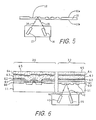
- Fig. 5 is a cross-sectional view which assists in explanation of another embodiment of the present invention wherein a code pattern 12 is formed by scribing a silicon surface 11a of a wafer 11 by a laser beam.
- the silicon surface 11a is scribed by the laser beam, the silicon material evaporates and the scribed area 12 is made rough, which forms the code pattern 12 in Fig. 5.
- an incident beam 14 from a light source 13 including infrared rays is irradiated onto a back surface 11b of the wafer 11, reflection from the silicon surface not subjected to laser scribing is stronger than that from a scribed area of the code pattern 12.
- the direction of a reflected beam 15 in the former case ideally, conforms to the law of optical reflection.
- the reflection in the latter case is irregular. Therefore, if the axis of a detector 16 for receiving reflected infrared rays is tilted away from the axis corresponding to reception of rays regularly reflected, the detector 16 substantially generates a signal corresponding to the irregular reflections from the code pattern area 12.
- a tungsten lamp which includes both visible and infrared rays or a helium-neon gas laser which abundantly includes 3.39 ⁇ m infrared rays can be used. Many other kinds of semiconductor LEDs and lasers for example can be used.
- a CCD sensor comprising a plurality of sensing elements can be utilized. The CCD sensor can be incorporated within an optical system to form the detector 6 or 16, and an output signal from the detector can then be subjected to a slice circuit and is converted to a signal corresponding to the code pattern (details are omitted in the Figures).
- the method explained in outline with reference to Fig. 5 is suitable for a case where each wafer is to be identified from an initial stage of wafer processing.
- the method outlined by Fig. 4 is suitable for a case where a plurality of wafers are collectively subjected to the same bulk wafer processes before a first metallization process. In this case, it is not necessary to identify each wafer but it is sufficient to identify each lot of wafers collectively processed until that time (up to the first metallization process). Thereafter, a code pattern is formed in the metal layer for identification of each wafer.
- the latter case is especially important for manufacturing ASICs or gate array integrated circuits, in which the patterning process of the metal layer is performed after receiving each customer's specification.
- Fig. 6 gives a cross-sectional view of a wafer for illustrating application of a method embodying the present invention, as explained in outline with reference to Fig. 5, to actual fabrication of integrated circuits, wherein a plurality of MOS FETS are formed as active elements in an active region on the wafer and two-level metal layers are required for the MOS FETS.
- a first region 30 a partial cross-sectional view of an area in which active elements are formed is given
- a second region 32 a view of an area in which a code pattern is formed, near an orientation flat edge of the wafer, is given.
- a bar code pattern is utilized as the code pattern because of its convenience for automatic formation and recognition.
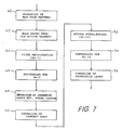
- Fig. 7 s a flow chart indicating processes involved in obtaining the structure of Fig. 6.
- the bar code pattern 12 is formed on a wafer 11 at an initial stage before wafer processes commence, as indicated at step 40. Then, the wafer is subjected to bulk wafer processes (step 42) until a first metallization step 44 is performed.
- step 42 most processes or steps for forming an active element, in this case a MOS FET, are performed conventionally.
- a thermally oxidized layer of SiO2 60 and a CVD (Chemical Vapor Deposition) layer of SiO2 61 are laminated on the bar code pattern 12 in the second region 32, as shown in Fig. 6.
- the wafer is subjected to a first metallization step (AL-I) 44 and a metal layer 62 of, for example, aluminum alloy is deposited thereon.
- the metal layer 62 in the first region 30 is patterned in step 46.
- An insulating layer 63 of, for example, PSG is formed in a step 48, a contact hole is formed in a step 50, and a second metal layer 64 (AL-II) is deposited in a step 52 and patterned in a step 54, and finally, a protective layer 65 is formed on the wafer in a step 56.
- A-II second metal layer 64
- a light source 13 of infrared rays disposed at the back side of the wafer irradiates an incident beam 14 onto the bar code pattern 12 in the second region 32 from the back side of the wafer.
- the bar code pattern is formed by laser scribing, the scribed surface of the silicon wafer exhibits a scabrous or roughened surface, therefore, the incident and penetrating light beam 14 through the wafer is reflected irregularly.
- reflection from the surface other than at scribed areas is regular and obeys optical laws.
- the detector when an optical axis of a detector 16 is tilted from a direction suitable for receiving regularly reflected light, the detector receives no (or very little) regularly reflected light. However, the detector can receive light reflected from the bar code pattern (the scribed surface areas).
- the above method is not affected by the laminated layers formed on the bar code pattern.
- the bar code pattern cannot be detected because of the existence of metal layers.
- a metal layer reflects almost all incident light, except when a window is formed in the metal layer over the bar code pattern.
- the bar code pattern can be identified regardless of the surface conditions of the wafer in the second region 32.
- FIG. 8 is a flow chart similar to that of Fig. 7.
- the bar code pattern is formed in a first metal layer (AL-I).
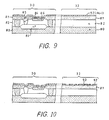
- Figs. 9 to 12 provide cross-sectional views corresponding to specific steps in Fig. 8.
- a bipolar transistor is formed in a first region 30, and the bar code pattern is formed in a second region 32.
- a p-type silicon wafer 80 and an n-type epitaxial layer 82 provide a silicon substrate, and an insulating layer 87 of thermally oxidized SiO2 and a first metal layer 92 (AL-I) are formed thereon in the second region 32.
- collector layers 81 and 85, a base region 84, and an emitter region 86 are formed in the first region 30, but the processes involved are conventional, and therefore details are omitted.
- the metal layer in the second region 32 is subjected to a step 74 for forming the bar code pattern by laser scribing, to provide a scribed pattern 93 forming the bar code pattern.
- the metal layer 92 is scribed by a laser beam, the metal evaporates and the thus exposed surface 93 of the insulating layer 87 becomes scabrous and roughened as shown in Fig. 10.
- the metal layer 92 in the first region 30 is patterned in step 76, forming a wiring layer.
- step 78 The entire surface of the wafer is covered by an insulating layer 94 in a step 78, and contact holes 96 are formed in the first region 30 (step 80), and a second metal layer 98 (AL-II) is deposited thereon (step 82) as shown in Fig. 11. Finally, the second metal layer 98 is patterned in a step 84 as shown in Fig 12.
- the embodiment of the present invention described above is especially suitable in relation to the manufacture of gate array integrated circuits, whereby identification of each wafer is not necessary before step 72 of Fig. 8. Identification of each wafer is, however, required for example in steps 76 and 84 because different pattern masks are used depending on different customer's requirements.
- a light source 3 of infrared rays disposed to the back side of the wafer irradiates an incident beam 4 onto the bar code pattern 93 in the second region 32 from the back side of the wafer.
- the bar code pattern is formed by laser scribing, parts of the metal layer are removed and the surface of the layer below the metal layer is scribed.
- the scribed surface exhibits a scabrous or roughened form, and therefore incident and penetrating infrared rays are reflected irregularly.
- the reflection from a back surface of the metal layer 92 is regular and in accordance with optical law. Therefore, when an optical axis of a detector 6 is tilted from a direction suitable for receiving regularly reflected light, the detector receives no or very little regularly reflected light. However, the detector receives irregularly reflected light from the bar code pattern 93.
- the detector may be disposed with its optical axis coincident with a direction suitable for receiving regularly reflected light.
- the detected light reflected from the bar code pattern is weaker than that from the metal layer.
- the signal of the bar code pattern can also be discriminated.
- the code pattern preferably a bar code pattern
- the code pattern is formed on or above a front surface of the semiconductor wafer, and a light beam including infrared rays is irradiated onto a bottom surface thereof.
- the infrared rays easily penetrate through the wafer (e.g. of silicon) and reflect from the bar code pattern formed on the front surface of the wafer.
- the reflect beam of infrared rays is received by a detector disposed to the back side of the wafer, and each wafer can be identified by decoding the received signal.
- the bar code pattern can be directly formed by scribing the wafer surface by a laser beam or scribing a metal layer deposited thereon.
Landscapes
- Testing Or Measuring Of Semiconductors Or The Like (AREA)
- Container, Conveyance, Adherence, Positioning, Of Wafer (AREA)
- Design And Manufacture Of Integrated Circuits (AREA)
Claims (10)
- Verfahren zum Identifizieren einer Halbleiterscheibe unter Verwendung eines Codemusters, das auf oder über einer die vordere Fläche der Scheibe definierenden Hauptoberfläche gebildet wird, und einer Lichtquelle sowie eines Detektors, die an der gegenüberliegenden, die hintere Fläche der Scheibe definierenden Hauptoberfläche angeordnet sind, welches Verfahren die Schritte umfaßt:(a) Bilden des Codemusters, um erste und zweite Zonen mit unterschiedlichen lichtreflektierenden Eigenschaften zu umfassen;(b) Bestrahlen der genannten hinteren Fläche der Halbleiterscheibe mit Infrarotstrahlen von der Lichtquelle, wobei die Infrarotstrahlen die Halbleiterscheibe zum Codemuster durchdringen und davon reflektiert werden;(c) Empfangen der genannten vom Codemuster reflektierten Infrarotstrahlen am Detektor; und(d) Identifizieren der Halbleiterscheibe durch Decodieren des empfangenen Lichtsignals.
- Verfahren nach Anspruch 1, bei welchem das Codemuster durch selektives Ritzen der vorderen Fläche der Halbleiterscheibe mit einem Laserstrahl gebildet wird, um aufgerauhte Bereiche zu erzeugen.
- Verfahren nach Anspruch 1, bei welchem das Codemuster durch Abscheiden einer Metallschicht auf oder über der vorderen Fläche der Halbleiterscheibe und selektives Ritzen der Metallschicht sowie Aufrauhen einer Fläche der Scheibe oder einer weiteren Schicht unter der Metallschicht mit einem Laserstrahl gebildet wird.
- Verfahren nach Anspruch 1, 2 oder 3 bei welchem ein aktives Element auf der vorderen Fläche der Halbleiterscheibe gebildet wird.
- Verfahren nach Anspruch 1, 2, 3 oder 4, bei welchem das Codemuster ein Strichcodemuster ist.
- Verfahren nach einem der vorhergehenden Ansprüche, bei welchem das Codemuster in einer Zone nahe eines flachen Orientierungsrandes der Halbleiterscheibe gebildet wird.
- Verfahren nach Anspruch 2 oder einem der Ansprüche 4 bis 6, wenn auf Anspruch 2 rückbezogen, bei welchem das Codemuster auf der vorderen Fläche der Halbleiterscheibe der Abscheidung einer Vielzahl von Schichten einschließlich einer Isolierschicht und einer Metallschicht darauf nach Schritt (a) ausgesetzt wird.
- Verfahren nach Anspruch 3 oder einem der Ansprüche 4 bis 6, wenn auf Anspruch 3 rückbezogen, bei welchem ein aktives Element auf der vorderen Fläche der Halbleiterscheibe gebildet wird, und die Metallschicht als eine erste Metallschicht des aktiven Elementes abgeschieden wird.
- Verfahren nach einem der vorhergehenden Ansprüche, bei welchem die optische Detektionsachse des Detektors zum Empfangen von reflektiertem Licht in Schritt (c) von der Richtung weg geneigt ist, die zum Empfangen von regelmäßig reflektiertem Licht geeignet ist, wodurch reflektiertes Licht von einem geritzten Bereich mit einer nicht-spiegelnden Reflexionseigenschaft durch den genannten Detektor empfangen wird.
- Verfahren nach einem der Ansprüche 1 bis 8, bei welchem die optische Detektionsachse des Detektors zum Empfangen von reflektiertem Licht in Schritt (c) eingerichtet ist, mit der Richtung zusammenzufallen, die zum Empfangen von regelmäßig reflektiertem Licht geeignet ist.
Applications Claiming Priority (2)
| Application Number | Priority Date | Filing Date | Title |
|---|---|---|---|
| JP255242/87 | 1987-10-09 | ||
| JP62255242A JPH0196920A (ja) | 1987-10-09 | 1987-10-09 | ウエーハの識別方法 |
Publications (3)
| Publication Number | Publication Date |
|---|---|
| EP0311087A2 EP0311087A2 (de) | 1989-04-12 |
| EP0311087A3 EP0311087A3 (en) | 1990-08-22 |
| EP0311087B1 true EP0311087B1 (de) | 1993-02-10 |
Family
ID=17276012
Family Applications (1)
| Application Number | Title | Priority Date | Filing Date |
|---|---|---|---|
| EP88116618A Expired - Lifetime EP0311087B1 (de) | 1987-10-09 | 1988-10-07 | Identifizierung von Halbleiterplättchen |
Country Status (5)
| Country | Link |
|---|---|
| US (1) | US4896034A (de) |
| EP (1) | EP0311087B1 (de) |
| JP (1) | JPH0196920A (de) |
| KR (1) | KR920003306B1 (de) |
| DE (1) | DE3878381T2 (de) |
Cited By (1)
| Publication number | Priority date | Publication date | Assignee | Title |
|---|---|---|---|---|
| US7544578B2 (en) | 2007-01-03 | 2009-06-09 | International Business Machines Corporation | Structure and method for stochastic integrated circuit personalization |
Families Citing this family (38)
| Publication number | Priority date | Publication date | Assignee | Title |
|---|---|---|---|---|
| CA2011296A1 (en) | 1989-05-15 | 1990-11-15 | Douglas C. Bossen | Presence/absence bar code |
| JPH0770453B2 (ja) * | 1989-10-05 | 1995-07-31 | 三菱電機株式会社 | 半導体装置の製造方法 |
| DE4107069A1 (de) * | 1991-03-06 | 1992-09-10 | Leuze Electronic Gmbh & Co | Verfahren zum lesen von strichkodierungen auf halbleiteroberflaechen |
| DE69227175T2 (de) * | 1991-12-20 | 1999-04-29 | Eastman Kodak Co., Rochester, N.Y. | Aufzeichnungsträger für ein optisches Informationssystem mit eingebettetem Identifikationskode |
| US5448499A (en) * | 1992-08-24 | 1995-09-05 | Olin Corporation | Mispour-misfill prevention apparatus and process |
| KR100293906B1 (ko) * | 1992-11-17 | 2001-11-22 | 가끼자끼다께요시 | 수지제박판수납용기 |
| TW230262B (de) * | 1992-12-24 | 1994-09-11 | American Telephone & Telegraph | |
| JPH06210987A (ja) * | 1993-01-19 | 1994-08-02 | Canon Inc | 非可視化情報記録媒体、非可視化情報検出装置並びに記録剤 |
| WO1994022104A1 (de) * | 1993-03-18 | 1994-09-29 | Siemens Aktiengesellschaft | Verfahren zur aufnahme von strichcodierungen |
| SE503738C2 (sv) * | 1994-10-03 | 1996-08-19 | Ericsson Telefon Ab L M | Sätt att bilda en streckkod |
| US5740066A (en) * | 1995-07-03 | 1998-04-14 | Motorola, Inc. | Electrical circuit board and circuit board assembly |
| DE19540348B4 (de) * | 1995-10-28 | 2007-01-11 | Micronas Gmbh | Verfahren zum Identifizieren von Bauelementen |
| US5956596A (en) * | 1995-11-06 | 1999-09-21 | Samsung Electronics Co., Ltd. | Method of forming and cleaning a laser marking region at a round zone of a semiconductor wafer |
| KR0147672B1 (ko) * | 1995-11-30 | 1998-08-01 | 김광호 | 웨이퍼를 용이하게 구별하기 위한 라벨 |
| US6938335B2 (en) | 1996-12-13 | 2005-09-06 | Matsushita Electric Industrial Co., Ltd. | Electronic component mounting method |
| EP0948250B1 (de) * | 1996-12-13 | 2006-02-08 | Matsushita Electric Industrial Co., Ltd. | Elektronisches bauteil und bestückungsverfahren und -vorrichtung |
| US5942805A (en) * | 1996-12-20 | 1999-08-24 | Intel Corporation | Fiducial for aligning an integrated circuit die |
| JP4344405B2 (ja) * | 1997-08-26 | 2009-10-14 | アベンティス・ファーマスーティカルズ・インコーポレイテッド | ピペリジノアルカノール−鬱血除去剤の組合せ用医薬組成物 |
| JP2000286437A (ja) * | 1998-06-12 | 2000-10-13 | Canon Inc | 太陽電池モジュールおよび製造方法 |
| EP0980098A1 (de) * | 1998-08-11 | 2000-02-16 | STMicroelectronics S.r.l. | Substrat aus Halbleitermaterial zur Verwendung in Herstellungprozessen von integrierten Schaltkreisen und Herstellungsverfahren eines solchen Substrats |
| FR2783971B1 (fr) * | 1998-09-30 | 2002-08-23 | St Microelectronics Sa | Circuit semi-conducteur comprenant des motifs en surface et procede de reglage d'un outil par rapport a cette surface |
| TW587332B (en) | 2000-01-07 | 2004-05-11 | Canon Kk | Semiconductor substrate and process for its production |
| US7253428B1 (en) * | 2000-04-04 | 2007-08-07 | Micron Technology, Inc. | Apparatus and method for feature edge detection in semiconductor processing |
| DE10038998A1 (de) | 2000-08-10 | 2002-02-21 | Bosch Gmbh Robert | Halbleiterbauelement und Verfahren zur Identifizierung eines Halbleiterbauelementes |
| KR20030008464A (ko) * | 2001-07-18 | 2003-01-29 | 삼성전자 주식회사 | 반도체 웨이퍼 |
| EP1989740B2 (de) * | 2006-02-28 | 2019-05-22 | Hanwha Q CELLS GmbH | Solarzellenmarkierverfahren und solarzelle |
| DE102007014969A1 (de) * | 2007-03-28 | 2008-10-02 | Infineon Technologies Ag | Vorrichtung zum Herstellen von Halbleiterbauelementen und Verfahren zum Alignment |
| US8247773B2 (en) | 2007-06-26 | 2012-08-21 | Yamaha Corporation | Method and apparatus for reading identification mark on surface of wafer |
| WO2009055474A1 (en) * | 2007-10-23 | 2009-04-30 | And, Llc | High reliability power systems and solar power converters |
| CN101904073B (zh) | 2007-10-15 | 2014-01-08 | Ampt有限公司 | 高效太阳能电力系统 |
| WO2010042124A1 (en) * | 2008-10-10 | 2010-04-15 | Ampt, Llc | Novel solar power circuits and powering methods |
| US9442504B2 (en) | 2009-04-17 | 2016-09-13 | Ampt, Llc | Methods and apparatus for adaptive operation of solar power systems |
| US9466737B2 (en) | 2009-10-19 | 2016-10-11 | Ampt, Llc | Solar panel string converter topology |
| CN102222601B (zh) * | 2010-04-14 | 2016-03-16 | 中芯国际集成电路制造(上海)有限公司 | 增强晶圆识别码清晰度的方法 |
| US9397497B2 (en) | 2013-03-15 | 2016-07-19 | Ampt, Llc | High efficiency interleaved solar power supply system |
| CN104253113B (zh) * | 2013-06-28 | 2017-07-11 | 上海华虹宏力半导体制造有限公司 | 一种测量时使用的定位标记及其识别方法 |
| US10020264B2 (en) * | 2015-04-28 | 2018-07-10 | Infineon Technologies Ag | Integrated circuit substrate and method for manufacturing the same |
| CN108630561B (zh) * | 2017-03-15 | 2021-10-15 | 北京北方华创微电子装备有限公司 | 基片表面的检测装置和检测方法、传片腔室 |
Citations (2)
| Publication number | Priority date | Publication date | Assignee | Title |
|---|---|---|---|---|
| US4010355A (en) * | 1974-06-10 | 1977-03-01 | Motorola, Inc. | Semiconductor wafer having machine readable indicies |
| EP0249762A1 (de) * | 1986-05-20 | 1987-12-23 | Fujitsu Limited | Identifizierung von Halbleiterscheiben mit Mustern des "Bar-code"-Typs |
Family Cites Families (6)
| Publication number | Priority date | Publication date | Assignee | Title |
|---|---|---|---|---|
| FR2179632B1 (de) * | 1972-04-14 | 1977-01-14 | Sescosem | |
| US4292576A (en) * | 1980-02-29 | 1981-09-29 | The United States Of America As Represented By The Secretary Of The Air Force | Mask-slice alignment method |
| US4368979A (en) * | 1980-05-22 | 1983-01-18 | Siemens Corporation | Automobile identification system |
| JPS5850728A (ja) * | 1981-09-19 | 1983-03-25 | Mitsubishi Electric Corp | 半導体装置の製造方法 |
| JPS5982741A (ja) * | 1982-11-04 | 1984-05-12 | Toshiba Corp | 集積回路の埋込層測定装置 |
| JPS60254769A (ja) * | 1984-05-31 | 1985-12-16 | Fujitsu Ltd | 半導体チツプの位置合せ方法 |
-
1987
- 1987-10-09 JP JP62255242A patent/JPH0196920A/ja active Pending
-
1988
- 1988-10-05 KR KR8812949A patent/KR920003306B1/ko not_active Expired
- 1988-10-06 US US07/254,100 patent/US4896034A/en not_active Expired - Lifetime
- 1988-10-07 EP EP88116618A patent/EP0311087B1/de not_active Expired - Lifetime
- 1988-10-07 DE DE8888116618T patent/DE3878381T2/de not_active Expired - Fee Related
Patent Citations (2)
| Publication number | Priority date | Publication date | Assignee | Title |
|---|---|---|---|---|
| US4010355A (en) * | 1974-06-10 | 1977-03-01 | Motorola, Inc. | Semiconductor wafer having machine readable indicies |
| EP0249762A1 (de) * | 1986-05-20 | 1987-12-23 | Fujitsu Limited | Identifizierung von Halbleiterscheiben mit Mustern des "Bar-code"-Typs |
Cited By (2)
| Publication number | Priority date | Publication date | Assignee | Title |
|---|---|---|---|---|
| US7544578B2 (en) | 2007-01-03 | 2009-06-09 | International Business Machines Corporation | Structure and method for stochastic integrated circuit personalization |
| US7838873B2 (en) | 2007-01-03 | 2010-11-23 | International Business Machines Corporation | Structure for stochastic integrated circuit personalization |
Also Published As
| Publication number | Publication date |
|---|---|
| KR890007365A (ko) | 1989-06-19 |
| DE3878381T2 (de) | 1993-06-03 |
| EP0311087A2 (de) | 1989-04-12 |
| US4896034A (en) | 1990-01-23 |
| KR920003306B1 (en) | 1992-04-27 |
| DE3878381D1 (de) | 1993-03-25 |
| JPH0196920A (ja) | 1989-04-14 |
| EP0311087A3 (en) | 1990-08-22 |
Similar Documents
| Publication | Publication Date | Title |
|---|---|---|
| EP0311087B1 (de) | Identifizierung von Halbleiterplättchen | |
| KR900008384B1 (ko) | 바아 코우드 패턴을 형성시킨 반도체 웨이퍼의 식별방법 및 반도체 장치의 제조방법 | |
| US6420792B1 (en) | Semiconductor wafer edge marking | |
| US5898227A (en) | Alignment targets having enhanced contrast | |
| JP2006527922A (ja) | エッジをベースにした識別機能を有する半導体ウエハ | |
| US7007855B1 (en) | Wafer identification mark | |
| US5135877A (en) | Method of making a light-emitting diode with anti-reflection layer optimization | |
| CA1277406C (en) | Semiconductor laser apparatus for optical head | |
| US20070170381A1 (en) | Semiconductor device structure that includes markings covered by visibly opaque materials | |
| US6573993B2 (en) | Apparatus and method for feature edge detection in semiconductor processing | |
| JPH0653258A (ja) | 表示装置の製造方法 | |
| JP2550671B2 (ja) | 半導体装置の製造方法とバーコードリーダ | |
| US6468704B1 (en) | Method for improved photomask alignment after epitaxial process through 90° orientation change | |
| JP2576711B2 (ja) | 半導体ウェーハ有無識別装置 | |
| US20040104361A1 (en) | Semiconductor wafer edge marking | |
| JPH05326360A (ja) | 半導体装置の製造方法及び製造装置 | |
| US7112821B2 (en) | Surface-emitting type light-emitting diode and fabrication method thereof | |
| CN101740323A (zh) | 半导体硅片对准标记制作方法及其制作的半导体硅片 | |
| KR20040040967A (ko) | 정렬마크, 이를 사용하는 정렬마크 검지시스템 및 이를이용한 검지방법 | |
| JP2597155Y2 (ja) | 反射型光結合器 | |
| JPH0571166B2 (de) | ||
| JPH0658885A (ja) | 異物検査装置およびそれを用いた異物検出方法 | |
| JPH05259021A (ja) | ウエハアライメントマークの形成方法 | |
| JP2002026375A (ja) | 光反射型センサ | |
| JPH09266165A (ja) | X線取り出し窓 |
Legal Events
| Date | Code | Title | Description |
|---|---|---|---|
| PUAI | Public reference made under article 153(3) epc to a published international application that has entered the european phase |
Free format text: ORIGINAL CODE: 0009012 |
|
| AK | Designated contracting states |
Kind code of ref document: A2 Designated state(s): DE FR GB |
|
| PUAL | Search report despatched |
Free format text: ORIGINAL CODE: 0009013 |
|
| AK | Designated contracting states |
Kind code of ref document: A3 Designated state(s): DE FR GB |
|
| RHK1 | Main classification (correction) |
Ipc: H01L 23/544 |
|
| 17P | Request for examination filed |
Effective date: 19901017 |
|
| 17Q | First examination report despatched |
Effective date: 19920102 |
|
| GRAA | (expected) grant |
Free format text: ORIGINAL CODE: 0009210 |
|
| AK | Designated contracting states |
Kind code of ref document: B1 Designated state(s): DE FR GB |
|
| REF | Corresponds to: |
Ref document number: 3878381 Country of ref document: DE Date of ref document: 19930325 |
|
| ET | Fr: translation filed | ||
| PLBE | No opposition filed within time limit |
Free format text: ORIGINAL CODE: 0009261 |
|
| STAA | Information on the status of an ep patent application or granted ep patent |
Free format text: STATUS: NO OPPOSITION FILED WITHIN TIME LIMIT |
|
| 26N | No opposition filed | ||
| REG | Reference to a national code |
Ref country code: GB Ref legal event code: IF02 |
|
| PGFP | Annual fee paid to national office [announced via postgrant information from national office to epo] |
Ref country code: GB Payment date: 20021002 Year of fee payment: 15 |
|
| PGFP | Annual fee paid to national office [announced via postgrant information from national office to epo] |
Ref country code: FR Payment date: 20021008 Year of fee payment: 15 |
|
| PGFP | Annual fee paid to national office [announced via postgrant information from national office to epo] |
Ref country code: DE Payment date: 20021011 Year of fee payment: 15 |
|
| PG25 | Lapsed in a contracting state [announced via postgrant information from national office to epo] |
Ref country code: GB Free format text: LAPSE BECAUSE OF NON-PAYMENT OF DUE FEES Effective date: 20031007 |
|
| PG25 | Lapsed in a contracting state [announced via postgrant information from national office to epo] |
Ref country code: DE Free format text: LAPSE BECAUSE OF NON-PAYMENT OF DUE FEES Effective date: 20040501 |
|
| GBPC | Gb: european patent ceased through non-payment of renewal fee |
Effective date: 20031007 |
|
| PG25 | Lapsed in a contracting state [announced via postgrant information from national office to epo] |
Ref country code: FR Free format text: LAPSE BECAUSE OF NON-PAYMENT OF DUE FEES Effective date: 20040630 |
|
| REG | Reference to a national code |
Ref country code: FR Ref legal event code: ST |