EP0253678A2 - Photoelektrischer Wandler - Google Patents
Photoelektrischer Wandler Download PDFInfo
- Publication number
- EP0253678A2 EP0253678A2 EP87306360A EP87306360A EP0253678A2 EP 0253678 A2 EP0253678 A2 EP 0253678A2 EP 87306360 A EP87306360 A EP 87306360A EP 87306360 A EP87306360 A EP 87306360A EP 0253678 A2 EP0253678 A2 EP 0253678A2
- Authority
- EP
- European Patent Office
- Prior art keywords
- electrode region
- control electrode
- region
- main electrode
- floating state
- Prior art date
- Legal status (The legal status is an assumption and is not a legal conclusion. Google has not performed a legal analysis and makes no representation as to the accuracy of the status listed.)
- Granted
Links
Images



Classifications
-
- H—ELECTRICITY
- H10—SEMICONDUCTOR DEVICES; ELECTRIC SOLID-STATE DEVICES NOT OTHERWISE PROVIDED FOR
- H10F—INORGANIC SEMICONDUCTOR DEVICES SENSITIVE TO INFRARED RADIATION, LIGHT, ELECTROMAGNETIC RADIATION OF SHORTER WAVELENGTH OR CORPUSCULAR RADIATION
- H10F39/00—Integrated devices, or assemblies of multiple devices, comprising at least one element covered by group H10F30/00, e.g. radiation detectors comprising photodiode arrays
- H10F39/10—Integrated devices
- H10F39/12—Image sensors
- H10F39/197—Bipolar transistor image sensors
-
- H—ELECTRICITY
- H04—ELECTRIC COMMUNICATION TECHNIQUE
- H04N—PICTORIAL COMMUNICATION, e.g. TELEVISION
- H04N25/00—Circuitry of solid-state image sensors [SSIS]; Control thereof
- H04N25/60—Noise processing, e.g. detecting, correcting, reducing or removing noise
- H04N25/67—Noise processing, e.g. detecting, correcting, reducing or removing noise applied to fixed-pattern noise, e.g. non-uniformity of response
-
- H—ELECTRICITY
- H04—ELECTRIC COMMUNICATION TECHNIQUE
- H04N—PICTORIAL COMMUNICATION, e.g. TELEVISION
- H04N25/00—Circuitry of solid-state image sensors [SSIS]; Control thereof
- H04N25/70—SSIS architectures; Circuits associated therewith
- H04N25/701—Line sensors
-
- H—ELECTRICITY
- H04—ELECTRIC COMMUNICATION TECHNIQUE
- H04N—PICTORIAL COMMUNICATION, e.g. TELEVISION
- H04N25/00—Circuitry of solid-state image sensors [SSIS]; Control thereof
- H04N25/70—SSIS architectures; Circuits associated therewith
- H04N25/76—Addressed sensors, e.g. MOS or CMOS sensors
-
- H—ELECTRICITY
- H04—ELECTRIC COMMUNICATION TECHNIQUE
- H04N—PICTORIAL COMMUNICATION, e.g. TELEVISION
- H04N25/00—Circuitry of solid-state image sensors [SSIS]; Control thereof
- H04N25/70—SSIS architectures; Circuits associated therewith
- H04N25/76—Addressed sensors, e.g. MOS or CMOS sensors
- H04N25/77—Pixel circuitry, e.g. memories, A/D converters, pixel amplifiers, shared circuits or shared components
-
- H—ELECTRICITY
- H04—ELECTRIC COMMUNICATION TECHNIQUE
- H04N—PICTORIAL COMMUNICATION, e.g. TELEVISION
- H04N25/00—Circuitry of solid-state image sensors [SSIS]; Control thereof
- H04N25/70—SSIS architectures; Circuits associated therewith
- H04N25/76—Addressed sensors, e.g. MOS or CMOS sensors
- H04N25/7795—Circuitry for generating timing or clock signals
Definitions
- the present invention relates to a photoelectric conversion device.
- An illustrative embodiment of the device has phototransistors and provides a photoelectric conversion device with improved photoelectric conversion characteristics and residual image effect, and reduced fixed pattern noises.
- Fig. 13A is a plan view showing the pattern of a photoelectric conversion device described in the Publications
- Fig. 13B is a sectional view along line I-I of Fig. 13A
- Fig. 13C is an equivalent circuit of a photosensor cell of the photoelectric conversion device.
- each photosensor cell of the photoelectric conversion device is constructed of an n-type silicon substrate 101 and electrically isolated from adjacent photosensor cells by an element isolation region 102 made of, for example, SiO2, Si3N4, polysilicon or the like.
- Each photosensor cell has the following constitutent elements: A p region 104 is formed by doping p-type impurity on an n ⁇ region 103 of low impurity concentration formed by the epitaxy method or the like. An n+ region 105 is formed in the p region 104 by the impurity diffusion method, the ion implantation method or the like. The p region 104 is n+ region 105 serve as the base and emitter of a bipolar transistor, respectively.
- a capacitor electrode 107 Formed on an oxide film 106 deposited on the n ⁇ region 103 with the above regions is a capacitor electrode 107 of predetermined area which faces the p region 104 with the oxide film 106 interposed therebetween and forms a capacitor Cox.
- the potential of the p region 104 in a floating state is controlled by a pulse voltage applied to the capacitor electrode 107.
- the photosensor cell is constructed further of an emitter electrode 108 connected to the n+ region 105, an interconnection 109 for reading a signal via the emitter electrode 108 and sending it to an external circuit, an interconnection 110 connected to the capacitor electrode 107, an n+ region 111 of high impurity concentration formed on the substrate 101, and an electrode 112 supplying a potential to the collector of the bipolar transistor.
- the p-base region 104 of the transistor is at a negative potential and at a floating state.
- carriers corresponding in amount to the incident light are accumulated in the p region 104 (accumulation operation).
- the base potential changes with the accumulated charge so that the emitter-collector current is controlled.
- an electric signal corresponding to the incident light quantity is read out of the emitter electrode 108 at a floating state (readout operation).
- the emitter electrode 108 is grounded and the capacitor electrode 107 is applied with a positive refresh pulse voltage.
- the p region 104 Upon application of a positive refresh pulse voltage, the p region 104 is forward biased relative to the n+ region 105 to thereby remove the accumulated carriers. After the refresh pulse falls, the p region 104 resumes a negative potential and hence a floating state (refresh operation). The above accumulation, readout and refresh operations are repeated.
- light-induced carriers are accumulated in the base p region 104 to control a current passing through the emitter and collector electrodes 108 and 112 in accordance with the accumulated charge quantity.
- the accumulated carriers are read after amplifying them by the amplification function of each cell, thereby achieving a high output and sensitivity, and less noise.
- the potential Vp of the base with light-induced carriers accumulated therein is given by Q/C, wherein Q represents the charge of carriers accumulated in the base region, and C represents a capacitor coupled to the base region.
- Q represents the charge of carriers accumulated in the base region
- C represents a capacitor coupled to the base region.
- Fig. 14 shows a change with time in base potential V B while a positive refresh pulse voltage is applied.
- the initial base potential when a positive refresh pulse votage is applied changes with the magnitude of an accumulated voltage Vp. Namely, the base potential which takes a negative potential at an initial condition changes in the positive direction by an accumulated voltage Vp during the accumulation operation, and upon application of a positive refresh pulse voltage to the capacitor electrode 107, the initial base potential rises by the amount corresponding to the accumulated voltage Vp.
- the period while an initial base potential is retained differs depending upon the magnitude of the initial base potential.
- the base potential V B gradually drops irrespective of its initial potential. Therefore, the base potential may be maintained at near zero volt irrespective of the accumulated voltage Vp on condition that a sufficiently long refresh time t is used. As a result, it is possible to make the base potential V B return to a predetermined negative potential when the positive refresh pulse voltage falls.
- the refresh time is limited so as to achieve a high speed operation.
- the initial base potential of a cell under high illumination is 0.8V, and under low illumination 0.4V.
- the base potential V B of the high illumination cell takes a predetermined residual potential V K
- the low illumination cell takes a residual potential V1 slightly lower than V K .
- the base potential V B of the low illumination cell takes a negative potential lower than the initial potential from which the following accumulation and readout operations start. Consequently, as the refresh operation repeats under such low illumination, the base residual potential gradually lowers. If the lower illumination cell with a lowered residual potential is changed to operate in high illumination, an output lower than that corresponding to an incident light quantity will be obtained. Namely, non-linear photoelectric conversion characteristics and residual image effect occur.
- the reason for this may be attributable to the deficit in carriers (holes) due to the recombination of holes in the base region. As the low illumination condition continues during which lost carriers (holes) cannot be replenished, the non-linear photoelectric conversion characteristics and residual effect becomes conspicuous.
- a method of removing carriers in the base regions has been proposed and filed by the present applicant.
- a MOS transistor 113 shown by dot-lines in Fig. 13C is turned on when a refresh operation is initiated to couple an initial base potential as shown in Fig. 14 to the base region and remove the carriers.
- the photoelectric conversion device in a phototransistor having a semiconductor region including two main electrode regions and a control electrode region formed between the two main electrode regions, and a capacitor for controlling the potential of the control electrode region in a floating state and accumulating carriers produced by an electromagnetic wave incident to the semiconductor region while controlling via the capacitor the potential of the control electrode region in a floating state, the photoelectric conversion device comprises: first control means for removing said carriers by controlling the potential of said control electrode region via said capacitor; second control means for removing the carriers of said first control means; and means for maintaining, immediately before the carrier removal operation by said second control means, the potential of said control electrode region at a constant potential for a predetermined period using a switch connected to said control electrode region.
- the capacitance C coupled to the control electrode region increases by Cox so that the potential Vp to be generated at the control electrode region lowers.
- dimension tolerance of capacitors Cox in a plurality of phototransistor arrays results in scattering of the light-induced potential Vp.
- K Cdg/(Cox + Cbe + Cbc) where Cbe represents a base-emitter capacitance of a bipolar transistor, Cbc represents a base-collector capacitance, and Cdg represents a gate-drain capacitance of the MOS transistor 113.
- the capacitor Cox is generally constructed as of MOS structure. Control of the interface between SiO2 and Si is difficult in most cases and in addition, the condition at the interface changes with an electric field, which is another reason of scattering of elements.
- An object of the present invention is to provide a photoelectric device capable of solving the above problems.
- the photoelectric conversion device in a phototransistor formed with a first main electrode region of a first conductivity type, a second main electrode region of a first conductivity type and a control electrode region of a second conductivity type opposite to the first conductivity type serving as an accumulation region for carriers induced by an electromagnetic wave, the photoelectric conversion device comprises first means for setting said control electrode region selectively at a constant potential and at a floating state and second means for setting said first main electrode region selectively at a low impedance state and at a floating state, whereby said first and second means control the carrier removal, accumulation and readout operations.
- the embodiment of the phototransistor of this invention includes a switch connected to the control electrode region, a voltage source connected to the switch, another switch connected to the second main electrode region, and another voltage source or a ground potential connected to the other switch. These switches control the base and emitter of the bipolar transistor. A capacitor for controlling the base potential is not used so that an improved output and a reduced scattering can be achieved.
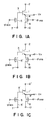
- Fig. 1A shows an equivalent circuit of an embodiment of a photoelectric conversion device according to the present invention.
- the collector of an NPN bipolar transistor 1 is connected to a positive voltage source, while the base p region 3 is connected to the drain of a p-channel MOS transistor.
- the source of the MOS transistor 5 is connected to a voltage source at potential V BG .
- the gate of the MOS transistor 5 is supplied with a pulse signal ⁇ RES .
- the emitter of the NPN transistor 1 is connected to an output terminal V X and to the drain of a MOS transistor 8 of which the source is connected to a constant voltage source 10.
- the gate of the MOS transistor 8 is applied with a pulse signal ⁇ VRS .
- the signal ⁇ RES is made high level and the transistor 5 is turned off so that the base p region 3 is set at an initial positive potential at a floating state.
- the signal ⁇ VRS is made low level and the transistor 8 is turned off so that the emitter electrode 4 is set at a zero potential and at a floating state.
- the collector electrode 2 is maintained at a positive potential. In this condition, upon application of light, carriers (in this case, holes) corresponding in the incident light quantity are accumulated in the base p region 3.
- a readout operation is carried out simultaneously with the accumulation operation via an emitter output terminal V X . That is an electric signal corresponding to the carriers accumulated in the base p region 3 is read from the emitter electrode 4 at a floating state.
- the emitter electrode 4 is set at a floating state by making the signal ⁇ VRS low level as shown by X1 in Fig. 2 and by making the transistor 8 turn off.
- the emitter electrode 4 is set to be connected to the constant voltage source 10 (including 0 potential) through MOS transistor 8 which is connected to the constant voltage source 10 by making the signal ⁇ VRS high level as shown by X2 and by making the transistor 8 turn on.
- the emitter electrode 4 is connected to, through the MOS transistor 8 connected to this electrode, the voltage source 10 having a potential sufficiently lower than the potential V BG of the voltage source connected to the source electrode 5 ⁇ .
- the gate electrode of the p-channel MOS transistor 5 is made high level to make it non-conductive.
- This period while the MOS transistor 8 connected to the emitter electrode is made conductive is called a second period (during T2 or T2 ⁇ shown in Fig. 2).
- the holes accumulated in the base p region 3 recombine with electrons injected from the emitter electrode 4 to the base p region 3 and are removed therefrom.
- the base potential at the start of the second period is V BG sufficiently higher than the residual potential V K irrespective of the degree of illuminance.
- the potential of the base p region 3 takes a constant potential V K irrespective of the degree of illuminance.
- the MOS transistor 8 connected to the emitter electrode 4 is made non-conductive and hence in a floating state so that the similar accumulation and readout operation as described before can proceed (refer to Fig. 2).
- NPN type bipolar transistor has been used in the above emboidment, but a PNP type bipolar transistor may also be used. In this case, holes are substituted for electrons and vice versa in the above description. The sign of voltage is also to be inverted.
- bipolar transistors of the above embodiment other semiconductors such as FETs (Field Effect Transistors) and SITs (Static Induction Transistors) may also be used.
- MOS switch connected to the base regions may be of a p-channel or n-channel type.
- An n-channel type MOS transistor connected to the base region is shown in Fig. 1B as the second embodiment.
- An SIT type phototransistor is shown in Fig. 1C as the third embodiment.
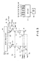
- Figs. 3 shows a fourth embodiment of the present invention.
- photoelectric cells shown in Fig. 1A are disposed in an array.
- Gates of MOS transistors 5 connected to the base of each bipolar transistor 1 are connected in common to a terminal 70 to which a pulse ⁇ RES is applied.
- Sources of the MOS transistors 5 are connected in common to a terminal 72 to which a potential V BG is supplied.
- Gates of MOS transistors 8 connected to the emitter of each bipolar transistor 1 are connected in common to a terminal 71 to which a pulse ⁇ VRS is applied.
- each transistor 1 is connected via each MOS transistor 11 to a corresponding light-shielded capacitor C T whose charge is supplied to an output amplifier 15 via each MOS transistor 12.
- the output signal from the amplifier 15 is outputtted at a terminal 76.
- the MOS transistors 12 are sequentially shifted by a shift register 13 which is inputted with shift pulses ⁇ SH from a terminal 79 to sequentially shift a high level signal output thereof.
- the gates of the MOS transistors 11 are connected in common to a terminal 73 to which a pulse ⁇ T is applied.
- the input of the amplifier 15 is connected via a MOS transistor 14 to a terminal 74 to which a constant potential V BH is supplied.
- MOS transistor 14 The gate of MOS transistor 14 is supplied with a pulse ⁇ HRS from a terminal 75.
- a clock driver 77 outputs, at predetermined timings in response to a clock signal from an oscillator 78, pulses ⁇ T , ⁇ RES , ⁇ VRS , ⁇ HRS and ⁇ SH and constant potential V BG and V BH , respectively to terminals 73 ⁇ , 70 ⁇ , 71 ⁇ , 75 ⁇ , 79 ⁇ , 72 ⁇ , and 74 ⁇ .
- the terminals 70 to 75 and 79 are connected respectively to terminals 70 ⁇ to 75 ⁇ and 79 ⁇ .
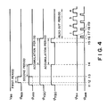
- Fig. 4 is a timing chart showing an example of pulse timings outputted from the clock driver 77.
- ⁇ T takes a high level so that the charge of the capacitor C T is discharged from the MOS transistor 8.
- ⁇ RES rises at time t3
- carriers accumulated in the base are gradually recombined and removes because ⁇ VRS is still high level. Since the base potential has been set at V BG as described before, the amount of carriers remaining in the base at time t4 is equal for each transistor irrespective of the amount of carriers remaining in the base before time t2.
- One pulse ⁇ HRS is supplied at time t7 to the MOS transistor 14 to turn it on and drain the residual charge in the parasitic capacitor on the output line 20 to the ground.
- one pulse SH is supplied at time t8 to the shift register 13 to start scanning each trnsistor 12. As the transistor 12 is made turned on, the charge accumulated in the capacitor C T is outputted at the terminal 76 via the amplifier 15. Immediately after one transistor 12 is made turned on to read the charge in the capacitor C T connected thereto as described before, the output line 20 is again cleared upon application of ⁇ HRS . These operations are repeated to sequentially read the signals photoelectrically converted during the period from time t4 to t6.
- the refresh and accumulation operations similar to those during the period from time t1 to t6 are carried out and thereafter, a readout operation similar to that after time t7 is carried out.
- the refresh, accumulation and readout operations are repeated in this order.
- the timing of ⁇ T (B) is used for an improved version of the above embodiment using the timing of ⁇ T (A).
- a low level is used during the period from time t4 to time t5. Consequently, carriers light-induced in the base region of the transistor are not accumulated in the capacitor C T , but accumulated in the base region it self of the transistor 1.
- ⁇ T (B) Upon application of pulse ⁇ T (B) during the period from time t5 to time t6, a signal corresponding to the carriers accumulated in the base region is transferred to the capacitor C T .
- the output increased by 20 to 30 % more than that by ⁇ T (A) and the range of scattering of sensitivities was remarkably narrowed.
- ⁇ VRS takes a high level during the period from time t1 to time t3, it may take a low level during the period. By doing so, a current flowing through the base-emitter during the period will be stopped, thus avoiding unnecessary comsuption of a power supply.
- Fig. 5 shows an example of the arrangement of a fifth embodiment of a photoelectric conversion device of line sensor type according to the present invention.
- the embodiment shown in Fig. 5 differs from that shown in Fig. 3 in the following points: in the embodiment shown in Fig. 3, the photosensor cells are supplied with ⁇ RES , ⁇ VRS and ⁇ T collectively to perform the refresh, accumulation and readout operations. Whereas in the embodiment shown in Fig. 5, each photosensor cell is independently driven during the refresh, accumulation and readout operations. In addition, in the later embodiment, the capacitor C T is not used for reading a signal from each photosensor cell.
- MOS transistors 12-1 to 12-n (n is integer) have same functions as the MOS transistors 12
- MOS transistors 1-1 to 1-n have same functions as the MOS transistors 1
- MOS transistors 5-1 to 5-7 have same functions as the MOS transistors 5
- MOS transistors 8-1 to 8-n have same functions as the MOS transistors 8.
- a shift register 13 sequentially outputs high level pulses ⁇ 1 to ⁇ n+2 in response to a shift pulse ⁇ SH .
- MOS transistors 5-m, 12-(m+1) and 8-(m-1) are arranged to be turned on by a common pulse (m+1), wherein m is an integer equal to and smaller than (n+1). Therefore, when a pulse ⁇ m is supplied, the potential of the bipolar transistor 1-(m-1) becomes V BG so that a readout operation for the transistor 1-m and a refresh operation for the transistor 1-(m-2) are carried out.
- a sequential refresh operation is effected with a delay of two pulses after the readout pulse.
- Fig. 6 shows a sixth embodiment of the present invention applied to an area image sensor.
- identical numbers are used for similar elements to those in Figs. 1 to 5.
- reference number 16 represents a vertical scan circuit
- reference numbers 17, 17 ⁇ and 18 represent MOS transistors.
- a driver circuit 77 ⁇ outputs pulses ⁇ SH , ⁇ HRS , ⁇ V1 to ⁇ V3 , ⁇ VRS , ⁇ T , V R , V RC and so on.
- Figs. 7 is a timing chart showing output pulses from the driver circuit 77 ⁇ shown in Fig. 6.
- ⁇ V1 is made high level and ⁇ V2 and ⁇ V3 are made low level so that the first row is selected among the matrix of rows and columns of the transistors 1.
- V RC is maintained high level during the period from time t11 to t12 so that the MOS transistors 5 are made turned on to set the bases of the transistors 1 at a collector potential (constant potential).
- V R and ⁇ VRS are made high level during the period from time t13 to time t14 and ⁇ T is made high level during the period from time t13 to t16.
- the MOS trnasistors 8, 18 and 11 are made turned on so that carriers of the base of the transistors 1 are extinguished by a current flowing through the emitters and the MOS transistors 8.
- a residual charge in the capacitor C T is drained to the ground.
- ⁇ VRS and V R are made low level to start the accumulation operation for the transistors at the first row.
- V R is maintained high level during the period from time t15 to time t16.
- the voltages corresponding to carriers having been accumulated in the transistors 1 at the second row is transferred to the capacitor C T via the MOS transistors 5.
- ⁇ V1 to ⁇ V3 are sequentially switched during one horizontal scan period by the vertical shift register 16 and circulate once during one vertical scan period.
- Figs. 8 and 9 show modifications of interconnection of each photoelectric cell shown in Fig. 6.
- the source of a MOS transistor 5 may be connected to the drain of a MOS transistor 18.
- V R and ⁇ VRS are made high level also during the period from time t11 to t13 shown in Fig. 7.
- V R and ⁇ VRS are made high level during the period from time t11 to time t13
- V RC is made high level during the period from time t11 to time t12
- the base of the transistor 1 is grounded to make residual carriers in the base recombine and extinguish.
- the source of the MOS transistor 5 shown in Fig. 5 is connected to a vertical signal line 19.
- ⁇ VRS is made high level during the period from time t11 to time t13 shown in the timing chart of Fig. 7.
- ⁇ VR is maintained low level.
- Fig. 10 shows a modification of the area image sensor shown in Fig. 6.
- the differences of this modification from the area image sensor shown in Fig. 6 are as follows: A horizontal signal line 20 is provided for each row and a MOS transistor 14 is provided for each horizontal signal line in order to selectively connect the horizontal line to the ground.
- the emitter of each transistor 1 may be connected selectively to the horizontal signal line via a MOS transistor 12 instead of the vertical signal line.
- a MOS transistor 12 is accordingly provided between the emitter of each transistor 1 and each horizontal signal line.
- the source of a MOS transistor 18 connected to the emitter of each transistor 1 is connected to a corresponding horizontal line instead of the vertical signal line.
- the vertical line shown in Fig. 6, the capacitors connected to the vertical line, the MOS transistors 11 and 8 and the like are omitted.
- MOS transistors 17 ⁇ are provided. And some other different points are included.
- ⁇ HRS ⁇ is slightly different from ⁇ HRS shown in the timing chart of Fig. 7. As shown in Fig. 11, ⁇ HRS ⁇ is maintained high level also during the period from time t13 to t14 shown in Fig. 7. V R ⁇ is maintained low level during the period from time t15 to t16.
- the timings of other pulses ⁇ SH , ⁇ V1 to ⁇ V3 and V RC are the same as those shown in Fig. 7.
- the base of the transistor 1 is maintained at the same potential as that of the collector during the period from time t11 to t12.
- carriers in the base are gradually drained from the ground via the MOS transistor 14.
- the carriers accumulated in the base of the second row transistors during one vertical scan period from time t15 to t16 are passed to the amplifier 15 via the signal line 20 and the MOS transistor 17 ⁇ and read out, by sequentially turning on the MOS transistors 12 by the horizontal scan circuit 13.
- Fig. 12 shows another example wherein one end of the MOS transistor 5 is connected to a signal line 20 instead of the collector to omit the MOS transistor 18.
- ⁇ HRS ⁇ is made high level during the period from t11 to t13 or from time t11 to t12, and high level during the period from time t13 to time t14. Namely, if the horizontal signal line 20 is maintained ground level while V RC is maintained high level during the period from t11 to t12, the residual carriers in the base are extinguished due to the zero level of the base.
Landscapes
- Engineering & Computer Science (AREA)
- Multimedia (AREA)
- Signal Processing (AREA)
- Transforming Light Signals Into Electric Signals (AREA)
- Solid State Image Pick-Up Elements (AREA)
- Optical Head (AREA)
- Glass Compositions (AREA)
- Amplifiers (AREA)
- Facsimile Heads (AREA)
- Photometry And Measurement Of Optical Pulse Characteristics (AREA)
Applications Claiming Priority (2)
| Application Number | Priority Date | Filing Date | Title |
|---|---|---|---|
| JP61168286A JPH0644619B2 (ja) | 1986-07-17 | 1986-07-17 | 光電変換装置 |
| JP168286/86 | 1986-07-17 |
Publications (3)
| Publication Number | Publication Date |
|---|---|
| EP0253678A2 true EP0253678A2 (de) | 1988-01-20 |
| EP0253678A3 EP0253678A3 (de) | 1988-06-01 |
| EP0253678B1 EP0253678B1 (de) | 1998-10-07 |
Family
ID=15865204
Family Applications (1)
| Application Number | Title | Priority Date | Filing Date |
|---|---|---|---|
| EP87306360A Expired - Lifetime EP0253678B1 (de) | 1986-07-17 | 1987-07-17 | Photoelektrischer Wandler |
Country Status (7)
| Country | Link |
|---|---|
| US (1) | US4810896A (de) |
| EP (1) | EP0253678B1 (de) |
| JP (1) | JPH0644619B2 (de) |
| AT (1) | ATE172056T1 (de) |
| CA (1) | CA1278079C (de) |
| DE (1) | DE3752221T2 (de) |
| ES (1) | ES2120941T3 (de) |
Cited By (8)
| Publication number | Priority date | Publication date | Assignee | Title |
|---|---|---|---|---|
| EP0274236A3 (de) * | 1986-12-09 | 1988-07-20 | Canon Kabushiki Kaisha | Photoelektrischer Wandler |
| EP0382568A3 (de) * | 1989-02-10 | 1991-09-18 | Canon Kabushiki Kaisha | Bildsensor und photoelektrisches Umwandlungsgerät zur Anwendung desselben |
| EP0327344A3 (de) * | 1988-02-02 | 1991-11-13 | Seiko Instruments Inc. | Festkörper-Bildsensor |
| EP0472066A1 (de) * | 1990-08-18 | 1992-02-26 | Seiko Instruments Inc. | Festkörper-Bildaufnahmevorrichtung |
| EP0473294A1 (de) * | 1990-08-07 | 1992-03-04 | Canon Kabushiki Kaisha | Photoumwandlerschaltung |
| EP0458460A3 (en) * | 1990-04-23 | 1992-10-14 | Canon Kabushiki Kaisha | Photoelectric conversion apparatus |
| US5262870A (en) * | 1989-02-10 | 1993-11-16 | Canon Kabushiki Kaisha | Image sensor in which reading and resetting are simultaneously performed |
| US5288988A (en) * | 1990-08-07 | 1994-02-22 | Canon Kabushiki Kaisha | Photoconversion device having reset control circuitry |
Families Citing this family (23)
| Publication number | Priority date | Publication date | Assignee | Title |
|---|---|---|---|---|
| JPS63206069A (ja) * | 1987-02-23 | 1988-08-25 | Fuji Photo Film Co Ltd | イメ−ジ・センサ |
| US4942474A (en) * | 1987-12-11 | 1990-07-17 | Hitachi, Ltd. | Solid-state imaging device having photo-electric conversion elements and other circuit elements arranged to provide improved photo-sensitivity |
| US5262850A (en) * | 1988-09-20 | 1993-11-16 | Canon Kabushiki Kaisha | Photoelectric converting device having reduced line sensor space |
| US5272345A (en) * | 1989-09-22 | 1993-12-21 | Ada Technologies, Inc. | Calibration method and apparatus for measuring the concentration of components in a fluid |
| JP2810526B2 (ja) * | 1989-11-21 | 1998-10-15 | キヤノン株式会社 | 光電変換装置及び該装置を搭載した装置 |
| US5241169A (en) * | 1989-11-21 | 1993-08-31 | Canon Kabushiki Kaisha | Photoelectric conversion device having an improved control electrode structure and apparatus equipped with same |
| US5260560A (en) * | 1990-03-02 | 1993-11-09 | Canon Kabushiki Kaisha | Photoelectric transfer device |
| JP3050583B2 (ja) * | 1990-10-17 | 2000-06-12 | ソニー株式会社 | 固体撮像装置 |
| US5262873A (en) * | 1990-11-07 | 1993-11-16 | Canon Kabushiki Kaisha | Image signal correcting in image data processing requiring only small memory capacity |
| US5281803A (en) * | 1990-11-26 | 1994-01-25 | Canon Kabushiki Kaisha | Image sensor and information processing apparatus |
| CA2056087C (en) * | 1990-11-27 | 1998-01-27 | Masakazu Morishita | Photoelectric converting device and information processing apparatus employing the same |
| JP2662105B2 (ja) * | 1991-04-08 | 1997-10-08 | キヤノン株式会社 | 密着型センサおよびイメージスキャナならびにファクシミリ |
| JP2768453B2 (ja) | 1992-03-03 | 1998-06-25 | キヤノン株式会社 | 固体撮像装置及びそれを用いた装置 |
| US5406332A (en) * | 1992-03-06 | 1995-04-11 | Canon Kabushiki Kaisha | Photoelectric converting device |
| JPH05335615A (ja) * | 1992-05-27 | 1993-12-17 | Canon Inc | 光電変換装置 |
| MY138010A (en) * | 1992-06-11 | 2009-04-30 | Canon Kk | Contact type image sensor, producing method of the same, and information processing apparatus |
| US5453611A (en) * | 1993-01-01 | 1995-09-26 | Canon Kabushiki Kaisha | Solid-state image pickup device with a plurality of photoelectric conversion elements on a common semiconductor chip |
| EP0616464B1 (de) * | 1993-03-15 | 1999-06-02 | Canon Kabushiki Kaisha | Signalprozessor |
| US5838176A (en) * | 1996-07-11 | 1998-11-17 | Foveonics, Inc. | Correlated double sampling circuit |
| TW421962B (en) | 1997-09-29 | 2001-02-11 | Canon Kk | Image sensing device using mos type image sensing elements |
| JP3467013B2 (ja) * | 1999-12-06 | 2003-11-17 | キヤノン株式会社 | 固体撮像装置 |
| US6940551B2 (en) | 2000-09-25 | 2005-09-06 | Foveon, Inc. | Active pixel sensor with noise cancellation |
| US6950131B1 (en) | 2000-09-26 | 2005-09-27 | Valley Oak Semiconductor | Simultaneous access and reset system for an active pixel sensor |
Family Cites Families (9)
| Publication number | Priority date | Publication date | Assignee | Title |
|---|---|---|---|---|
| JPS5528456B2 (de) * | 1972-11-08 | 1980-07-28 | ||
| JPS55105480A (en) * | 1979-02-07 | 1980-08-13 | Hitachi Ltd | Solid state pickup device |
| JPS5850030B2 (ja) * | 1979-03-08 | 1983-11-08 | 日本放送協会 | 光電変換装置およびそれを用いた固体撮像板 |
| US4445117A (en) * | 1981-12-28 | 1984-04-24 | Hughes Aircraft Company | Transistorized focal plane having floating gate output nodes |
| JPS59107569A (ja) * | 1982-12-13 | 1984-06-21 | Fuji Photo Film Co Ltd | 一次元半導体撮像装置 |
| JPH0744661B2 (ja) * | 1982-12-14 | 1995-05-15 | オリンパス光学工業株式会社 | 固体撮像装置 |
| JPS59108476A (ja) * | 1982-12-14 | 1984-06-22 | Junichi Nishizawa | 2次元固体撮像装置及びその読出し方法 |
| US4686554A (en) * | 1983-07-02 | 1987-08-11 | Canon Kabushiki Kaisha | Photoelectric converter |
| JPS61157184A (ja) * | 1984-12-28 | 1986-07-16 | Canon Inc | 光電変換装置 |
-
1986
- 1986-07-17 JP JP61168286A patent/JPH0644619B2/ja not_active Expired - Fee Related
-
1987
- 1987-07-14 US US07/073,220 patent/US4810896A/en not_active Expired - Lifetime
- 1987-07-15 CA CA000542160A patent/CA1278079C/en not_active Expired - Lifetime
- 1987-07-17 ES ES87306360T patent/ES2120941T3/es not_active Expired - Lifetime
- 1987-07-17 AT AT87306360T patent/ATE172056T1/de not_active IP Right Cessation
- 1987-07-17 EP EP87306360A patent/EP0253678B1/de not_active Expired - Lifetime
- 1987-07-17 DE DE3752221T patent/DE3752221T2/de not_active Expired - Fee Related
Cited By (13)
| Publication number | Priority date | Publication date | Assignee | Title |
|---|---|---|---|---|
| EP0274236A3 (de) * | 1986-12-09 | 1988-07-20 | Canon Kabushiki Kaisha | Photoelektrischer Wandler |
| US4866293A (en) * | 1986-12-09 | 1989-09-12 | Canon Kabushiki Kaisha | Photoelectric converting apparatus to prevent the outflow of excess carriers |
| EP0667707A3 (de) * | 1986-12-09 | 1995-09-06 | Canon Kk | |
| EP0327344A3 (de) * | 1988-02-02 | 1991-11-13 | Seiko Instruments Inc. | Festkörper-Bildsensor |
| US5262870A (en) * | 1989-02-10 | 1993-11-16 | Canon Kabushiki Kaisha | Image sensor in which reading and resetting are simultaneously performed |
| EP0382568A3 (de) * | 1989-02-10 | 1991-09-18 | Canon Kabushiki Kaisha | Bildsensor und photoelektrisches Umwandlungsgerät zur Anwendung desselben |
| EP0458460A3 (en) * | 1990-04-23 | 1992-10-14 | Canon Kabushiki Kaisha | Photoelectric conversion apparatus |
| US5184006A (en) * | 1990-04-23 | 1993-02-02 | Canon Kabushiki Kaisha | Photoelectric conversion apparatus having clock signals of different frequencies |
| EP0473294A1 (de) * | 1990-08-07 | 1992-03-04 | Canon Kabushiki Kaisha | Photoumwandlerschaltung |
| US5288988A (en) * | 1990-08-07 | 1994-02-22 | Canon Kabushiki Kaisha | Photoconversion device having reset control circuitry |
| US5424529A (en) * | 1990-08-07 | 1995-06-13 | Canon Kabushiki Kaisha | Photoconversion device including reset means and biasing means |
| US5146074A (en) * | 1990-08-18 | 1992-09-08 | Seiko Instruments Inc. | Solid state imaging device |
| EP0472066A1 (de) * | 1990-08-18 | 1992-02-26 | Seiko Instruments Inc. | Festkörper-Bildaufnahmevorrichtung |
Also Published As
| Publication number | Publication date |
|---|---|
| DE3752221T2 (de) | 1999-03-25 |
| ATE172056T1 (de) | 1998-10-15 |
| DE3752221D1 (de) | 1998-11-12 |
| CA1278079C (en) | 1990-12-18 |
| EP0253678B1 (de) | 1998-10-07 |
| US4810896A (en) | 1989-03-07 |
| JPS6324664A (ja) | 1988-02-02 |
| EP0253678A3 (de) | 1988-06-01 |
| ES2120941T3 (es) | 1998-11-16 |
| JPH0644619B2 (ja) | 1994-06-08 |
Similar Documents
| Publication | Publication Date | Title |
|---|---|---|
| US4810896A (en) | Photoelectric conversion device with reduced fixed pattern noises | |
| EP0489724B1 (de) | Anordnung und Verfahren zum photoelektrischen Umformen von Licht in elektrische Signale | |
| EP0455311B1 (de) | Bildsensoranordnung | |
| US5587738A (en) | Solid-state image pickup device having plural switches for subtracting a stored signal from a pixel output | |
| US5276407A (en) | Sense amplifier | |
| US5097305A (en) | Integrating photosensor and imaging system having wide dynamic range | |
| EP0272152B1 (de) | Signalausleseschaltung | |
| USRE34309E (en) | Image sensor device having plural photoelectric converting elements | |
| EP0277016B1 (de) | Photovoltaischer Wandler | |
| US5933188A (en) | Photoelectric conversion apparatus and method with reset | |
| EP0593139A2 (de) | Fotoelektrische Umwandlungsvorrichtung | |
| US4922138A (en) | Scan circuit using a plural bootstrap effect for forming scan pulses | |
| US5386108A (en) | Photoelectric conversion device for amplifying and outputting photoelectrically converted signal, and a method thereof | |
| EP0274236B1 (de) | Photoelektrischer Wandler | |
| JPH11312798A (ja) | リニアイメージセンサ | |
| US6618086B1 (en) | Linear image sensor | |
| US5126814A (en) | Photoelectric converter with doped capacitor region | |
| JP3548301B2 (ja) | 固体撮像装置及びその駆動方法 | |
| JPH084131B2 (ja) | 光電変換装置 | |
| JPH0746839B2 (ja) | 光電変換装置 | |
| JPH0697408A (ja) | 光電変換装置及びその製造方法 | |
| JP2990475B2 (ja) | 光電変換装置及びその制御方法 | |
| JPH0682818B2 (ja) | 固体撮像装置 | |
| JPS63120566A (ja) | 光電変換装置 | |
| JPH0523547B2 (de) |
Legal Events
| Date | Code | Title | Description |
|---|---|---|---|
| PUAI | Public reference made under article 153(3) epc to a published international application that has entered the european phase |
Free format text: ORIGINAL CODE: 0009012 |
|
| AK | Designated contracting states |
Kind code of ref document: A2 Designated state(s): AT BE CH DE ES FR GB GR IT LI LU NL SE |
|
| PUAL | Search report despatched |
Free format text: ORIGINAL CODE: 0009013 |
|
| AK | Designated contracting states |
Kind code of ref document: A3 Designated state(s): AT BE CH DE ES FR GB GR IT LI LU NL SE |
|
| 17P | Request for examination filed |
Effective date: 19881019 |
|
| 17Q | First examination report despatched |
Effective date: 19920312 |
|
| GRAG | Despatch of communication of intention to grant |
Free format text: ORIGINAL CODE: EPIDOS AGRA |
|
| GRAG | Despatch of communication of intention to grant |
Free format text: ORIGINAL CODE: EPIDOS AGRA |
|
| GRAG | Despatch of communication of intention to grant |
Free format text: ORIGINAL CODE: EPIDOS AGRA |
|
| GRAH | Despatch of communication of intention to grant a patent |
Free format text: ORIGINAL CODE: EPIDOS IGRA |
|
| GRAH | Despatch of communication of intention to grant a patent |
Free format text: ORIGINAL CODE: EPIDOS IGRA |
|
| GRAA | (expected) grant |
Free format text: ORIGINAL CODE: 0009210 |
|
| ITF | It: translation for a ep patent filed | ||
| AK | Designated contracting states |
Kind code of ref document: B1 Designated state(s): AT BE CH DE ES FR GB GR IT LI LU NL SE |
|
| REF | Corresponds to: |
Ref document number: 172056 Country of ref document: AT Date of ref document: 19981015 Kind code of ref document: T |
|
| REG | Reference to a national code |
Ref country code: CH Ref legal event code: NV Representative=s name: BOVARD AG PATENTANWAELTE Ref country code: CH Ref legal event code: EP |
|
| REF | Corresponds to: |
Ref document number: 3752221 Country of ref document: DE Date of ref document: 19981112 |
|
| REG | Reference to a national code |
Ref country code: ES Ref legal event code: FG2A Ref document number: 2120941 Country of ref document: ES Kind code of ref document: T3 |
|
| ET | Fr: translation filed | ||
| PLBE | No opposition filed within time limit |
Free format text: ORIGINAL CODE: 0009261 |
|
| STAA | Information on the status of an ep patent application or granted ep patent |
Free format text: STATUS: NO OPPOSITION FILED WITHIN TIME LIMIT |
|
| 26N | No opposition filed | ||
| REG | Reference to a national code |
Ref country code: GB Ref legal event code: IF02 |
|
| PGFP | Annual fee paid to national office [announced via postgrant information from national office to epo] |
Ref country code: ES Payment date: 20030701 Year of fee payment: 17 |
|
| PGFP | Annual fee paid to national office [announced via postgrant information from national office to epo] |
Ref country code: GB Payment date: 20030703 Year of fee payment: 17 |
|
| PGFP | Annual fee paid to national office [announced via postgrant information from national office to epo] |
Ref country code: CH Payment date: 20030709 Year of fee payment: 17 Ref country code: AT Payment date: 20030709 Year of fee payment: 17 |
|
| PGFP | Annual fee paid to national office [announced via postgrant information from national office to epo] |
Ref country code: SE Payment date: 20030717 Year of fee payment: 17 |
|
| PGFP | Annual fee paid to national office [announced via postgrant information from national office to epo] |
Ref country code: GR Payment date: 20030718 Year of fee payment: 17 |
|
| PGFP | Annual fee paid to national office [announced via postgrant information from national office to epo] |
Ref country code: FR Payment date: 20030721 Year of fee payment: 17 |
|
| PGFP | Annual fee paid to national office [announced via postgrant information from national office to epo] |
Ref country code: DE Payment date: 20030723 Year of fee payment: 17 |
|
| PGFP | Annual fee paid to national office [announced via postgrant information from national office to epo] |
Ref country code: NL Payment date: 20030731 Year of fee payment: 17 |
|
| PGFP | Annual fee paid to national office [announced via postgrant information from national office to epo] |
Ref country code: LU Payment date: 20030804 Year of fee payment: 17 |
|
| PGFP | Annual fee paid to national office [announced via postgrant information from national office to epo] |
Ref country code: BE Payment date: 20030811 Year of fee payment: 17 |
|
| PG25 | Lapsed in a contracting state [announced via postgrant information from national office to epo] |
Ref country code: LU Free format text: LAPSE BECAUSE OF NON-PAYMENT OF DUE FEES Effective date: 20040717 Ref country code: GB Free format text: LAPSE BECAUSE OF NON-PAYMENT OF DUE FEES Effective date: 20040717 Ref country code: AT Free format text: LAPSE BECAUSE OF NON-PAYMENT OF DUE FEES Effective date: 20040717 |
|
| PG25 | Lapsed in a contracting state [announced via postgrant information from national office to epo] |
Ref country code: SE Free format text: LAPSE BECAUSE OF NON-PAYMENT OF DUE FEES Effective date: 20040718 |
|
| PG25 | Lapsed in a contracting state [announced via postgrant information from national office to epo] |
Ref country code: ES Free format text: LAPSE BECAUSE OF NON-PAYMENT OF DUE FEES Effective date: 20040719 |
|
| PG25 | Lapsed in a contracting state [announced via postgrant information from national office to epo] |
Ref country code: LI Free format text: LAPSE BECAUSE OF NON-PAYMENT OF DUE FEES Effective date: 20040731 Ref country code: CH Free format text: LAPSE BECAUSE OF NON-PAYMENT OF DUE FEES Effective date: 20040731 Ref country code: BE Free format text: LAPSE BECAUSE OF NON-PAYMENT OF DUE FEES Effective date: 20040731 |
|
| BERE | Be: lapsed |
Owner name: *CANON K.K. Effective date: 20040731 |
|
| PG25 | Lapsed in a contracting state [announced via postgrant information from national office to epo] |
Ref country code: NL Free format text: LAPSE BECAUSE OF NON-PAYMENT OF DUE FEES Effective date: 20050201 Ref country code: DE Free format text: LAPSE BECAUSE OF NON-PAYMENT OF DUE FEES Effective date: 20050201 |
|
| PG25 | Lapsed in a contracting state [announced via postgrant information from national office to epo] |
Ref country code: GR Free format text: LAPSE BECAUSE OF NON-PAYMENT OF DUE FEES Effective date: 20050203 |
|
| EUG | Se: european patent has lapsed | ||
| GBPC | Gb: european patent ceased through non-payment of renewal fee |
Effective date: 20040717 |
|
| REG | Reference to a national code |
Ref country code: CH Ref legal event code: PL |
|
| PG25 | Lapsed in a contracting state [announced via postgrant information from national office to epo] |
Ref country code: FR Free format text: LAPSE BECAUSE OF NON-PAYMENT OF DUE FEES Effective date: 20050331 |
|
| NLV4 | Nl: lapsed or anulled due to non-payment of the annual fee |
Effective date: 20050201 |
|
| REG | Reference to a national code |
Ref country code: FR Ref legal event code: ST |
|
| PG25 | Lapsed in a contracting state [announced via postgrant information from national office to epo] |
Ref country code: IT Free format text: LAPSE BECAUSE OF NON-PAYMENT OF DUE FEES;WARNING: LAPSES OF ITALIAN PATENTS WITH EFFECTIVE DATE BEFORE 2007 MAY HAVE OCCURRED AT ANY TIME BEFORE 2007. THE CORRECT EFFECTIVE DATE MAY BE DIFFERENT FROM THE ONE RECORDED. Effective date: 20050717 |
|
| REG | Reference to a national code |
Ref country code: ES Ref legal event code: FD2A Effective date: 20040719 |
|
| BERE | Be: lapsed |
Owner name: *CANON K.K. Effective date: 20040731 |