EP0489724B1 - Anordnung und Verfahren zum photoelektrischen Umformen von Licht in elektrische Signale - Google Patents
Anordnung und Verfahren zum photoelektrischen Umformen von Licht in elektrische Signale Download PDFInfo
- Publication number
- EP0489724B1 EP0489724B1 EP92200671A EP92200671A EP0489724B1 EP 0489724 B1 EP0489724 B1 EP 0489724B1 EP 92200671 A EP92200671 A EP 92200671A EP 92200671 A EP92200671 A EP 92200671A EP 0489724 B1 EP0489724 B1 EP 0489724B1
- Authority
- EP
- European Patent Office
- Prior art keywords
- charge carriers
- base region
- region
- emitter
- stored
- Prior art date
- Legal status (The legal status is an assumption and is not a legal conclusion. Google has not performed a legal analysis and makes no representation as to the accuracy of the status listed.)
- Expired - Lifetime
Links
Images

Classifications
-
- H—ELECTRICITY
- H10—SEMICONDUCTOR DEVICES; ELECTRIC SOLID-STATE DEVICES NOT OTHERWISE PROVIDED FOR
- H10F—INORGANIC SEMICONDUCTOR DEVICES SENSITIVE TO INFRARED RADIATION, LIGHT, ELECTROMAGNETIC RADIATION OF SHORTER WAVELENGTH OR CORPUSCULAR RADIATION
- H10F39/00—Integrated devices, or assemblies of multiple devices, comprising at least one element covered by group H10F30/00, e.g. radiation detectors comprising photodiode arrays
- H10F39/10—Integrated devices
- H10F39/12—Image sensors
- H10F39/197—Bipolar transistor image sensors
-
- H—ELECTRICITY
- H04—ELECTRIC COMMUNICATION TECHNIQUE
- H04N—PICTORIAL COMMUNICATION, e.g. TELEVISION
- H04N25/00—Circuitry of solid-state image sensors [SSIS]; Control thereof
- H04N25/60—Noise processing, e.g. detecting, correcting, reducing or removing noise
- H04N25/62—Detection or reduction of noise due to excess charges produced by the exposure, e.g. smear, blooming, ghost image, crosstalk or leakage between pixels
- H04N25/621—Detection or reduction of noise due to excess charges produced by the exposure, e.g. smear, blooming, ghost image, crosstalk or leakage between pixels for the control of blooming
-
- H—ELECTRICITY
- H04—ELECTRIC COMMUNICATION TECHNIQUE
- H04N—PICTORIAL COMMUNICATION, e.g. TELEVISION
- H04N25/00—Circuitry of solid-state image sensors [SSIS]; Control thereof
- H04N25/70—SSIS architectures; Circuits associated therewith
- H04N25/76—Addressed sensors, e.g. MOS or CMOS sensors
Definitions
- the present invention relates to a device and method of photoelectrically converting light into an electrical signal wherein a potential at a control electrode region of a semiconductor transistor is controlled through a capacitor to store carriers excited with light in the control electrode region, thereby controlling an output from the semiconductor transistor.
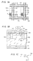
- Fig. 1A is a plan view of a photoelectric transducer device described in EP-A-0 132 076, Fig. 1B is a sectional view of the device taken along the line I - I thereof, and Fig. 1C is a diagram of an equivalent circuit thereof.
- photoelectric transducer cells are arranged on an n-type silicon substrate 101.
- the photoelectric transducer cells are electrically insulated by an element isolation region 102 made of SiO 2 , Si 3 N 4 or polysilicon.
- Each photoelectric transducer cell has the following construction.
- a p-type impurity is doped to form a p-type region 104 on an n -type region 103 having a low impurity concentration formed by an epitaxial technique or the like.
- An n + -type region 105 is formed in the p-type region 104 by impurity diffusion or ion implantation.
- the p- and n + -type regions 104 and 105 serve as the base and emitter of each bipolar transistor.
- An oxide film 106 is formed on the n - -type region 103.
- a capacitor electrode 107 having a predetermined area is formed on the oxide film 106.
- the capacitor electrode 107 opposes the p-type region 104, with the oxide film 106 interposed therebetween, thereby constituting a capacitor C ox .
- the potential of the p-type region 104 in the floating state is controlled.
- An emitter electrode 108 connected to the n + -type region 105, a wiring 109 for extracting the signal from the emitter electrode 108, and a wiring 110 connected to the capacitor electrode 107 are formed at the upper surface side of the substrate 101.
- An n + -type region 111 having a high impurity concentration and an electrode 112 for applying a voltage to the collector of a bipolar transistor are sequentially formed on the lower surface of the substrate 101.
- the p-type region 104 as the base region of the bipolar transistor is set in the initial state of a negative potential.
- Light 113 is incident on the p-type region 104 and carriers corresponding to the amount of light are stored in the p-type region 104 (storage operation).
- the base potential is changed by the charged carriers.
- the change in base potential controls a current supplied to an emitter-collector path, and an electrical signal having a level corresponding to the amount of incident light is extracted from the floating emitter electrode 108 (read operation).
- the emitter electrode 108 is grounded and a refresh positive voltage pulse is supplied to the capacitor electrode 107.
- the p-type region 104 Upon application of this positive voltage, the p-type region 104 is forward-biased with respect to the n + -type region 105, thereby removing the charged carriers. When the refresh pulse falls, the p-type region 104 returns to the initial state of the negative potential (refresh operation). The cycle of storage, read, and refresh operations is repeated.
- the carriers generated upon reception of light are stored in the p-type region 104 as the base region, and the current supplied between the emitter and collector electrodes 108 and 112 is controlled by the stored carriers. Therefore, the stored carriers are amplified by the amplification function of each cell, and the amplified carriers are read out. Therefore, a high output with high sensitivity and low noise can be obtained.
- a potential Vp generated by the base by the carriers stored in the base upon light excitation is given by Q/C where Q is the charge of the carriers stored in the base, and C is the capacitance connected to the base.
- Fig. 2 is a graph showing changes in base potential Vb during the application of the positive refresh voltage as a function of time.
- the initial base potential at the time of the application of the refresh pulse varies according to the magnitude of the storage voltage Vp.
- the negative potential in the initial state is changed in the positive direction by the storage voltage Vp during the storage operation.
- the initial base potential is greater than a potential after refresh by the storage voltage Vp.
- the time for which the initial base potential is maintained varies according to the magnitude of the initial base potential.
- the base potential Vb is decreased at a common rate regardless of the initial base potential. If the refresh time t is sufficiently long, the base potential Vb can be controlled to be substantially 0 V regardless of the magnitude of the storage voltage Vp. Therefore, the base potential Vb returns to the predetermined negative potential of the initial state when the refresh pulse falls.
- the initial base potential of a cell receiving a large amount of light is 0.8 V and that the initial base potential of a cell receiving a small amount of light is 0.4 V.
- the base potential Vb of the cell receiving a large amount of light becomes the predetermined residual potential Vk.
- the base potential Vb of the cell receiving a small amount of light becomes a residual potential Vl lower than the predetermined residual potential Vk.
- the refresh pulse falls, the base potential Vb of the cell receiving a small amount of light becomes lower than the negative potential of the initial state. From a potential lower than the initial negative potential, storage and read operations are started.
- the refresh operation is repeated in a low illuminance state, the residual potential of the base is gradually decreased. Even if a high illuminance state is obtained, the resultant output has a level lower than that corresponding to the amount of incident light. In other words, the after image phenomenon occurs due to the following reason.
- the holes in the base region are recombined to result in their shortage. If the shortage of holes cannot be compensated for a long period of time, i.e., if the low illuminance state continues for a long period of time, the after image phenomenon typically occurs.
- Fig. 3 is a schematic circuit diagram of an area sensor using a conventional photoelectric transducer device.
- conventional photoelectric transducer cells 120 of a 3 x 3 matrix are arranged in the area sensor.
- Emitter electrodes 108 of the cells 120 are connected to corresponding vertical lines in units of columns.
- Capacitor electrodes 107 are connected to horizontal lines in units of rows.
- a positive voltage from a vertical scanning unit 121 is applied to the photoelectric transducer cells 120 to perform read access or refresh operation in units of rows.
- EP-A-0132076 also proposes an arrangement in which the emitter of the bipolar transistor also functions as the drain region of an MOS transistor, and the source region of the MOS transistor is connected to the base region of the bipolar transistor by a conductor. At the time of the refresh operation the emitter (and therefore the drain region) is grounded and then the MOS transistor is turned on, so that a current flows to bring the base to zero potential. Then the MOS transistor is turned off and the base is refreshed by applying the refresh pulse to the capacitor electrode. In another embodiment EP-A-0132076 proposes that the refresh pulse is not used, and the base is refreshed only by applying a voltage to the base through an MOS transistor, which may be constructed as described above or may be completely separate from the emitter.
- EP-A-0206649 (which was published on 30 December 1986, after the filing date of the present application, but which has a filing date earlier than the filing date of the present application and a priority date earlier than the priority dates of the present application) proposes that the photoelectric transducer cell includes an additional semiconductor region, of the same conductivity type as the base region, underneath a cell isolation region, so as to form a pnpn structure.
- the additional semiconductor region acts as the emitter of a secondary bipolar transistor, the base of which is formed by the collector of the main bipolar transistor and the collector of which is formed by the base of the main bipolar transistor.
- This secondary bipolar transistor is used for injecting carriers into the base region of the main bipolar transistor before the refresh pulse is applied to the capacitor electrode.
- the emitters of the main bipolar transistors are connected to vertical lines which are connected through transistors to storage capacitors, and then through further transistors to an output line.
- the emitter electrodes are also connected to ground through further transistors, for grounding the emitter electrodes during the refresh pulse.
- An embodiment of the present invention provides a device and method of photoelectrically converting light into an electrical signal, wherein a residual potential is not decreased even if refresh operation is repeated, and an after image phenomenon can be eliminated.
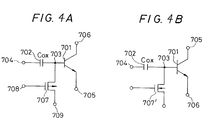
- Fig. 4A is an equivalent circuit diagram of a photoelectric transducer device used in an embodiment of the present invention.
- a p-type base region 703 of an npn bipolar transistor 701 is connected to a capacitor electrode 704 through a capacitor 702.
- the base region 703 is connected to the drain of a p-channel MOS transistor 707.
- the p-type base region 703 is set in the initial negative potential, the emitter electrode 705 is set at zero potential in the floating state, and the capacitor electrode 704 is set at zero potential.
- the collector electrode 706 is maintained at a positive potential.
- the gate electrode 708 of the p-channel MOS transistor 707 is set at a positive potential, and the p-channel MOS transistor 707 is rendered nonconductive. In this state, upon reception of light, carriers (holes in this case) corresponding to the amount light are stored in the p-type base region 703.
- the emitter electrode 705 is set in the floating state, and a positive read voltage pulse is applied to the capacitor electrode 704. As previously mentioned, an electrical signal corresponding to the amount of incident light is read out to the emitter electrode 705.
- the capacitor electrode 704 is set at zero potential
- the emitter electrode 705 is set in the floating state or at zero potential
- a source electrode 709 of the p-channel MOS transistor 707 is set at a proper potential, e.g., the ground potential.
- a negative pulse is applied to the gate electrode 708 of the p-channel MOS transistor 707. If the potential of the p-type base region 703 is lower than that of the source electrode 709 in the dark state or a state wherein an amount of light is small, the holes are injected into the p-type base region 703 to increase its potential.
- the potential of the p-type base region 703 is set to be equal to that of the source electrode 709.
- the potential of the source electrode 709 is set such that the potential of the p-type base region 703 is sufficiently higher than the residual potential Vk even in the dark state.
- the emitter electrode 705 is grounded, the gate electrode 708 of the p-channel MOS transistor 707 is set at a positive potential, and the p-channel MOS transistor 707 is rendered nonconductive.
- the refresh pulse is applied to the capacitor electrode 704
- the holes stored in the p-type base region 703 are recombined with the electrons injected from the emitter electrode 705 to the p-type base region 703, thus eliminating the holes. Since the potential of the p-type base region 703 is sufficiently high due to the hole injection operation even in the dark state, the initial base potential upon application of the refresh pulse is sufficiently higher than the residual potential Vk regardless of the amount of incident light (Fig. 2).
- the potential of the p-type base region 703 is set at the predetermined potential Vk regardless of the amount of incident light. In this state, when the positive refresh pulse falls, the p-type base region 703 is set at the predetermined initial negative potential.
- the holes in the p-type base region 703 are not subject to shortage even if the refresh operation is repeated. Therefore, nonlinearity of the photoelectric transducer characteristics and the after image phenomenon with a small amount of light can be completely prevented.
- the base region as the control electrode has a p conductivity type, and thus the carriers are holes.
- the base region as the main control electrode of a pnp bipolar transistor has an n conductivity type, the carriers are electrons.
- the means for injecting the carriers in the p-type base region is a p-channel MOS transistor.
- other means may be used in place of the p-channel MOS transistor.
- an n-channel MOS transistor may be used.
- the control means for controlling the potential of the control electrode region through the capacitor to dissipate the carriers (holes) stored therein is the means for grounding the emitter region, applying the refresh pulse to the capacitor electrode, and then injecting electrons from the emitter region, thereby recombining the electrons and the holes.
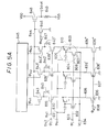
- Fig. 5A is a circuit diagram of an image pickup device having photoelectric transducer cells arranged in a one-dimensional manner
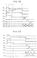
- Fig. 5B is a timing chart for explaining the operation of the image pickup device in Fig. 5A.
- collector electrodes 809 are commonly connected and receive a positive voltage.
- Capacitor electrodes 804 are commonly connected to a terminal 831 through a horizontal line 830.
- a read/ refresh pulse signal ⁇ R is applied to the terminal 831.
- Emitter electrodes 805 are respectively connected to vertical lines 835, 835', and 835".
- a gate electrode 808 of the transistor 807 is connected to a terminal 833 through a horizontal line 832 and receives a pulse signal ⁇ c for hole injection.
- a source electrode of the transistor 807 is connected to a terminal 834 for receiving a hole injection voltage Vc.
- the vertical lines 835, 835', and 835" are respectively grounded through transistors 836, 836', and 836".
- the gate electrodes of the transistors 836, 836', and 836" are commonly connected to a terminal 838 through a line 837.
- a signal ⁇ vc is applied to the terminal 838.
- the vertical lines 835, 835', and 835" are respectively connected to charge storage capacitors 840, 840', and 840" through transistors 839, 839', and 839" and to an output line 844 through transistors 843, 843', and 843".
- the gate electrodes of the transistors 839, 839', and 839" are commonly connected to a terminal 842 through a line 841.
- a signal ⁇ T is applied to the terminal 842.
- the gate electrodes of the transistors 843, 843', and 843" are connected to the parallel output terminals of a shift register 845. Signals ⁇ H1, ⁇ H2, and ⁇ H3 respectively appear at the parallel output terminals.
- the output line 844 is grounded through a transistor 846 for refreshing the output line 844 and connected to the gate electrode of a transistor 848 serving as an output amplifier and having an output terminal 849.
- the gate electrode of the refresh transistor 846 is connected to a terminal 847.
- a signal ⁇ Hc is applied to the terminal 847.
- the pulse signals ⁇ T and ⁇ vc rise to turn on the transistors 839, 839', 839", 836, 836', and 836".
- the emitter electrodes 805 of the photoelectric transducer cells 810 and the vertical lines 835, 835', and 835" are grounded, thereby removing the residual charges from the charge storage capacitors 840, 840', and 840" and the vertical lines 835, 835', and 835".
- the signal ⁇ c rises so that the potential Vc applied to the terminal 834 is applied to the base region 803 of each photoelectric transducer cell 810.
- the holes are injected into the base region 803 of each photoelectric transducer cell 810 held in the dark state or receiving a small amount of light.
- the potentials at the base regions of the photoelectric transducer cells are set to be substantially equal to each other (hole injection operation).
- the signal ⁇ c falls and at time t2 the signal ⁇ R rises to apply the positive refresh voltage to the capacitor electrodes 804 of the photoelectric transducer cells 810. Since the emitter electrodes are grounded, the refresh operation is performed in the same manner as described with reference to Fig. 4A.
- the signal ⁇ R falls at time t3
- the p-type base regions 803 of the photoelectric transducer cells 810 are reset in the initial negative potential state.
- the signal ⁇ vc falls to turn off the transistor 836, 836', and 836".
- the signal ⁇ R rises again to apply the positive read voltage to the capacitor electrodes 804 of the photoelectric transducer cells 810.
- the holes of the electron-hole pairs excited by incident light are stored in the p-type base regions of the photoelectric transducer cells 810.
- the base potential of each cell is increased by the storage voltage component corresponding to the amount of light, and at the same time, the read operation is performed.
- the read signals corresponding to the optical information of the photoelectric transducer cells 810 are respectively stored in the charge storage capacitors 840, 840', and 840".
- the store operation in this case is conducted under the condition that respective cells are forward-biased between base and emitter thereof.
- the signals ⁇ T and ⁇ R fall to turn off the transistors 839, 839', and 839".
- the signal ⁇ Hc rises to remove the residual charge from the output line 844, and then the signal ⁇ Hc falls.
- the signal ⁇ H1 output from the first output terminal of the shift register 845 rises to turn on the transistor 843, so that the read signal stored in the charge storage capacitor 840 is read out onto the output line 844.
- the readout signal appears at the terminal 849 through the transistor 848. Subsequently, the signal ⁇ Hc rises, and the output line 844 is grounded through the transistor 846, thereby removing the residual charge.
- the signals 843' and 843" output from the shift register 845 sequentially rise to read out the read signals from the charge storage capacitors 840' and 840" onto the output line 844. Every time a read signal appears, the pulse signal ⁇ Hc rises to refresh the output line 844. In this manner, the read signals from all the photoelectric transducer cells 810 serially appear at the terminal 849 through the transistor 848.
- Fig. 5C is a timing chart for explaining another operation of the image pickup device in Fig. 5A.
- Fig. 5C shows the operation mode wherein the signal ⁇ R which rises at time t2 does not fall at time t3, and other signal timings are the same as those in Fig. 5B.
- a store operation is conducted under the condition that respective cells are forward-biased between base and emitter thereof, the signals generated by the transistors 805 of the photoelectric transducer cells are always read out onto the vertical lines 835, 835', and 835". Such read operation can be allowed.
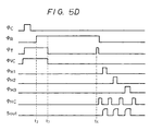
- Fig. 5D is a timing chart for explaining still another operation of the embodiment as shown in Fig. 5A.
- Fig. 5D shows the operation mode wherein the signal ⁇ T which has not fallen at the time t3, falls at the time t3 and rises again at the time t4 at which the store operation is completed.
- An operation of another timings is the same as that of Fig. 5C.
- the signals produced at the transistors 805 of respective cells are readout to only the vertical lines 835, 835', and 835".
- the emitter current of the transistor 805 also is reduced.
- the signals stored in bases of respective cells can be read out to the capacitors 840, 840', and 840".
- the signals including low current operation irregularity of the transistor 805 produced during the long store time are removed.
- Signals without operation irregularity of transistors of respective cells can be read out to the capacitors 840, 840', and 840".
- the photoelectric transducer device of this embodiment as described above, a transistor and the like is formed in the control electrode region of the semiconductor transistor, and thus the potential of the control electrode is controlled. Therefore, the carriers can be injected into the control electrode at the proper time.
- the potential of the control electrode region can be kept sufficiently high at the beginning of refreshing.
- the potential of the control electrode region at the end of refreshing can be maintained at a desired predetermined value.
- the conventional nonlinearity of the characteristics and the after image phenomenon of the photoelectric transducer can be improved.
Landscapes
- Engineering & Computer Science (AREA)
- Multimedia (AREA)
- Signal Processing (AREA)
- Transforming Light Signals Into Electric Signals (AREA)
- Solid State Image Pick-Up Elements (AREA)
- Fire-Detection Mechanisms (AREA)
- Optical Head (AREA)
- Switches Operated By Changes In Physical Conditions (AREA)
- Optical Communication System (AREA)
Claims (11)
- Photoelektrische Wandlervorrichtung miteiner Vielzahl photoelektrischer Wandlerzellen (810), wobei jede Zelle umfaßt:einen Bipolartransistor mit einem Basisbereich, einem Emitterbereich, einem Kollektorbereich und einer an den Basisbereich kapazitiv gekoppelte Steuerelektrode und wobei der Transistor in der Lage ist, infolge einfallender elektromagnetischer Strahlung Ladungsträger in dem Basisbereich anzusammeln, ein Signal in Bezug zu der Menge der in dem Basisbereich gespeicherten Ladungsträger aus dem Emitterbereich bereitzustellen und den Basisbereich durch die Neutralisierung der darin gespeicherten Ladungsträger aufzufrischen, undeinen Transistor mit isolierendem Gate (707, 707') zur Injektion von Ladungsträgern in den Basisbereich mindestens in dem Fall, daß eine relativ geringe Menge Ladungsträger darin gespeichert ist,eine Vielzahl von Speicherkondensatoren (840) zum Empfangen und Speichern der Signale aus dem Emitterbereich,eine Vielzahl von ersten weiteren Transistoren (839) zur Kopplung der Emitterbereiche an die Speicherkondensatoren,eine Ausgangsleitung (844),eine Vielzahl von zweiten weiteren Transistoren (843) zur Kopplung der Speicherkondensatoren an die Ausgangsleitung,eine Vielzahl von dritten weiteren Transistoren (836) zur Kopplung der Emitterbereiche an ein festes Potential, undeine Steuereinrichtung zum Steuern des Bipolar-transistors und des Transistors mit isolierendem Gate jeder Zelle, und zum Steuern der ersten, zweiten und dritten weiteren Transistoren, unddie Steuereinrichtung bezüglich jeder Zelle angeordnet ist, um(a) den Transistor mit isolierendem Gate zu veranlassen, Ladungsträger in den Basisbereich zu injizieren, nachdem ein Signal von dem Emitterbereich ausgegeben wurde, mindestens in dem Fall, daß der Basisbereich eine relative geringe Menge an Ladungsträgern in sich gespeichert hat,(b) aufeinanderfolgend einen Auffrischimpuls zu bewirken, der an die Steuerelektrode zur Neutralisierung der im Basisbereich gespeicherten Ladungsträger angelegt wird,(c) den jeweiligen dritten weiteren Transistor (836) zu veranlassen, den Emitterbereich an ein festes Potential zu koppeln, während er den an die Steuerelektrode anzulegenden Auffrischimpuls bewirkt, und(d) eine Spannung (R) über die Steuerelektrode an den Basisbereich anzulegen, damit der Basis-Emitter-Übergang während der Ladungsträgeransammlung in Durchlaßrichtung vorgespannt ist, so daß das Signal von dem Emitterbereich während der Ladungsträgeransammlung ausgegeben wird.
- Vorrichtung nach Anspruch 1, in der die Steuereinrichtung zur Steuerung der ersten weiteren Transistoren (839) in den leitenden Zustand dient, so daß die von dem Emitterbereich ausgegeben Signale während der Ladungsträgeransammlung in den Speicherkondensatoren (840) gespeichert werden.
- Vorrichtung nach Anspruch 1, in der aufeinanderfolgend die Steuereinrichtung zur Steuerung der ersten weiteren Transistoren (839) in den nichtleitenden Zustand, so daß die von dem Emitterbereich ausgegebenen Signale während der Ladungsträgeransammlung nicht in den Speicherkondensatoren (840) gespeichert werden, und zur Steuerung der ersten weiteren Transistoren (839) in den leitenden Zustand vorgesehen ist, so daß die Signale in den Speicherkondensatoren gespeichert werden.
- Vorrichtung nach einem der vorstehenden Ansprüche, in der die Steuereinrichtung vorgesehen ist, zum veranlassen des dritten weiteren Transistors (836), den Emitterbereich auf dem festen Potential zu halten, bevor und während dieser den Transistor mit dem isolierenden Gate veranlaßt, Ladungsträger in den Basisbereich zu injizieren.
- Verfahren zum Betreiben der photoelektrischen Wandlervorrichtung mit
einer Vielzahl photoelektrischer Wandlerzellen (810),
wobei jede Zelle umfaßt:einen Bipolartransistor mit einem Basisbereich, einem Emitterbereich, einem Kollektorbereich und einer an den Basisbereich kapazitiv gekoppelte Steuerelektrode, und wobei der Transistor in der Lage ist, infolge einfallender elektromagnetischer Strahlung Ladungsträger in dem Basisbereich anzusammeln, ein Signal in Bezug zu der Menge der in dem Basisbereich gespeicherten Ladungsträger aus dem Emitterbereich bereitzustellen und den Basisbereich durch die Neutralisierung der darin gespeicherten Ladungsträger aufzufrischen, undeinen Transistor mit isolierendem Gate (707, 707') zur Injektion von Ladungsträgern in den Basisbereich mindestens in dem Fall, daß eine relativ geringe Menge Ladungsträger darin gespeichert ist,eine Vielzahl von Speicherkondensatoren (840) zum Empfangen und Speichern der Signale aus dem Emitterbereich,eine Vielzahl von ersten weiteren Transistoren (839) zur Kopplung der Emitterbereiche an die Speicherkondensatoren,eine Ausgangsleitung (844),eine Vielzahl von zweiten weiteren Transistoren (843) zur Kopplung der Speicherkondensatoren an die Ausgangsleitung, undeine Vielzahl von dritten weiteren Transistoren (836) zur Kopplung der Emitterbereiche an ein festes Potential, und wobeidas Verfahren die folgenden Schritte bezüglich jeder Zelle aufweist,(a) Injzieren von Ladungsträgern in den Basisbereich, nachdem ein Signal von dem Emitterbereich ausgegeben wurde, mindestens in dem Fall, wenn der Basisbereich eine relative geringe Menge an Ladungsträgern in sich gespeichert hat,(b) aufeinanderfolgendes Anlegen eines Auffrischimpulses an die Steuerelektrode zur Neutralisierung der im Basisbereich gespeicherten Ladungsträger,(c) Halten des Emitterbereichs an ein festes Potential mittels des jeweiligen dritten weiteren Transistors (836), während des Schrittes zur Anlegung eines Auffrischimpulses, und(d) Anlegen einer Spannung (R) über die Steuerelektrode an den Basisbereich, damit der Basis-Emitter-Übergang während der Ladungsträgeransammlung in Durchlaßrichtung vorgespannt ist, um das Signal von dem Emitterbereich während der Ladungsträgeransammlung auszugeben. - Verfahren nach Anspruch 5, mit dem Schritt des Versetzens der ersten weiteren Transistoren (839) in den leitenden Zustand und Speicherns der Signale in den Speicherkondensatoren (840) während der Ladungsträgeransammlung.
- Verfahren nach Anspruch 5, mit dem Schritt des Versetzens der ersten weiteren Transistoren (839) in den nichtleitenden Zustand und nicht Speichern der Signale in den Speicherkondensatoren (840) während der Ladungsträgeransammlung, und nachfolgend des Versetzens der ersten weiteren Transistoren (839) in den leitenden Zustand und Speicherns der Signale in den Speicherkondensatoren (840).
- Verfahren nach einem der Ansprüche 5 bis 7, wobei der Emitterbereich vor und während des Schrittes der Injizierung von Ladungsträgern in den Basisbereich auf einem festen Potential gehalten wird.
- Verfahren nach einem der Ansprüche 5 bis 8, wobei Ladungsträger in Schritt (a) in den Basisbereich injiziert werden, unabhängig von der in ihm gespeicherten Menge an Ladungsträgern.
- Verfahren nach einem der Ansprüche 5 bis 8, wobei nur dann Ladungsträger in Schritt (a) in den Basisbereich injiziert werden, wenn die in ihm gespeicherte Menge an Ladungsträgern unterhalb eines Schwellenwertes ist.
- Verfahren nach Anspruch 10, wobei Ladungsträger aus dem Basisbereich entfernt anstatt in ihn injiziert werden, wenn die in ihm gespeicherte Menge an Ladungsträgern oberhalb des Schwellenwertes ist.
Applications Claiming Priority (5)
| Application Number | Priority Date | Filing Date | Title |
|---|---|---|---|
| JP60252654A JPH06101814B2 (ja) | 1985-11-13 | 1985-11-13 | 光電変換装置 |
| JP252654/85 | 1985-11-13 | ||
| JP60269873A JPH0746839B2 (ja) | 1985-11-29 | 1985-11-29 | 光電変換装置 |
| JP269873/85 | 1985-11-29 | ||
| EP86308863A EP0222624B1 (de) | 1985-11-13 | 1986-11-13 | Anordnung und Verfahren zum photoelektrischen Umformen von Licht in elektrische Signale |
Related Parent Applications (2)
| Application Number | Title | Priority Date | Filing Date |
|---|---|---|---|
| EP86308863A Division EP0222624B1 (de) | 1985-11-13 | 1986-11-13 | Anordnung und Verfahren zum photoelektrischen Umformen von Licht in elektrische Signale |
| EP86308863.9 Division | 1986-11-13 |
Publications (3)
| Publication Number | Publication Date |
|---|---|
| EP0489724A2 EP0489724A2 (de) | 1992-06-10 |
| EP0489724A3 EP0489724A3 (en) | 1992-12-16 |
| EP0489724B1 true EP0489724B1 (de) | 1999-03-03 |
Family
ID=26540816
Family Applications (2)
| Application Number | Title | Priority Date | Filing Date |
|---|---|---|---|
| EP86308863A Expired - Lifetime EP0222624B1 (de) | 1985-11-13 | 1986-11-13 | Anordnung und Verfahren zum photoelektrischen Umformen von Licht in elektrische Signale |
| EP92200671A Expired - Lifetime EP0489724B1 (de) | 1985-11-13 | 1986-11-13 | Anordnung und Verfahren zum photoelektrischen Umformen von Licht in elektrische Signale |
Family Applications Before (1)
| Application Number | Title | Priority Date | Filing Date |
|---|---|---|---|
| EP86308863A Expired - Lifetime EP0222624B1 (de) | 1985-11-13 | 1986-11-13 | Anordnung und Verfahren zum photoelektrischen Umformen von Licht in elektrische Signale |
Country Status (5)
| Country | Link |
|---|---|
| US (1) | US4847668A (de) |
| EP (2) | EP0222624B1 (de) |
| AT (2) | ATE80964T1 (de) |
| CA (1) | CA1289242C (de) |
| DE (2) | DE3650714T2 (de) |
Families Citing this family (27)
| Publication number | Priority date | Publication date | Assignee | Title |
|---|---|---|---|---|
| US5771070A (en) * | 1985-11-15 | 1998-06-23 | Canon Kabushiki Kaisha | Solid state image pickup apparatus removing noise from the photoelectric converted signal |
| JPH084127B2 (ja) * | 1986-09-30 | 1996-01-17 | キヤノン株式会社 | 光電変換装置 |
| US4914519A (en) * | 1986-09-19 | 1990-04-03 | Canon Kabushiki Kaisha | Apparatus for eliminating noise in a solid-state image pickup device |
| US5737016A (en) * | 1985-11-15 | 1998-04-07 | Canon Kabushiki Kaisha | Solid state image pickup apparatus for reducing noise |
| US4866293A (en) * | 1986-12-09 | 1989-09-12 | Canon Kabushiki Kaisha | Photoelectric converting apparatus to prevent the outflow of excess carriers |
| FR2638042A1 (fr) * | 1988-10-14 | 1990-04-20 | Thomson Csf | Procede pour reduire la remanence d'un phototransistor, notamment de type nipin |
| US5040041A (en) * | 1988-10-20 | 1991-08-13 | Canon Kabushiki Kaisha | Semiconductor device and signal processing device having said device provided therein |
| JPH02275670A (ja) * | 1989-01-18 | 1990-11-09 | Canon Inc | 光電変換装置および画像読取装置 |
| JP2878376B2 (ja) * | 1990-02-28 | 1999-04-05 | キヤノン株式会社 | 光電変換装置 |
| US5283428A (en) * | 1990-11-27 | 1994-02-01 | Canon Kabushiki Kaisha | Photoelectric converting device and information processing apparatus employing the same |
| US5324958A (en) * | 1991-02-19 | 1994-06-28 | Synaptics, Incorporated | Integrating imaging systgem having wide dynamic range with sample/hold circuits |
| US5260592A (en) * | 1991-02-19 | 1993-11-09 | Synaptics, Incorporated | Integrating photosensor and imaging system having wide dynamic range with varactors |
| US5406332A (en) * | 1992-03-06 | 1995-04-11 | Canon Kabushiki Kaisha | Photoelectric converting device |
| DE69427051T2 (de) | 1993-05-28 | 2001-09-06 | Canon K.K., Tokio/Tokyo | Photoelektrische Umwandlungsanordnung |
| US5552619A (en) * | 1995-05-10 | 1996-09-03 | National Semiconductor Corporation | Capacitor coupled contactless imager with high resolution and wide dynamic range |
| JPH09129864A (ja) | 1995-10-30 | 1997-05-16 | Canon Inc | 半導体装置及びそれを用いた半導体回路、相関演算装置、信号処理システム |
| JP3774499B2 (ja) | 1996-01-24 | 2006-05-17 | キヤノン株式会社 | 光電変換装置 |
| US5838176A (en) * | 1996-07-11 | 1998-11-17 | Foveonics, Inc. | Correlated double sampling circuit |
| US5786623A (en) * | 1996-10-22 | 1998-07-28 | Foveonics, Inc. | Bipolar-based active pixel sensor cell with metal contact and increased capacitive coupling to the base region |
| US5760458A (en) * | 1996-10-22 | 1998-06-02 | Foveonics, Inc. | Bipolar-based active pixel sensor cell with poly contact and increased capacitive coupling to the base region |
| US6940551B2 (en) | 2000-09-25 | 2005-09-06 | Foveon, Inc. | Active pixel sensor with noise cancellation |
| JP2002289879A (ja) * | 2001-03-27 | 2002-10-04 | Toshiba Corp | ダイオード |
| JP5688756B2 (ja) * | 2008-12-25 | 2015-03-25 | 国立大学法人静岡大学 | 半導体素子及び固体撮像装置 |
| JP5648922B2 (ja) * | 2009-10-05 | 2015-01-07 | 国立大学法人静岡大学 | 半導体素子及び固体撮像装置 |
| JP5818455B2 (ja) | 2011-02-17 | 2015-11-18 | キヤノン株式会社 | 固体撮像装置およびその製造方法 |
| JP5893550B2 (ja) | 2012-04-12 | 2016-03-23 | キヤノン株式会社 | 撮像装置及び撮像システム |
| US10553633B2 (en) * | 2014-05-30 | 2020-02-04 | Klaus Y.J. Hsu | Phototransistor with body-strapped base |
Family Cites Families (5)
| Publication number | Priority date | Publication date | Assignee | Title |
|---|---|---|---|---|
| US3660667A (en) * | 1970-06-22 | 1972-05-02 | Rca Corp | Image sensor array in which each element employs two phototransistors one of which stores charge |
| JPS59108344A (ja) * | 1982-12-14 | 1984-06-22 | Olympus Optical Co Ltd | 固体撮像素子 |
| US4686554A (en) * | 1983-07-02 | 1987-08-11 | Canon Kabushiki Kaisha | Photoelectric converter |
| GB2170675B (en) * | 1984-12-28 | 1989-12-13 | Canon Kk | Image sensing apparatus |
| JPH0760888B2 (ja) * | 1985-06-12 | 1995-06-28 | キヤノン株式会社 | 光電変換装置 |
-
1986
- 1986-11-12 CA CA000522797A patent/CA1289242C/en not_active Expired - Lifetime
- 1986-11-13 AT AT86308863T patent/ATE80964T1/de not_active IP Right Cessation
- 1986-11-13 AT AT92200671T patent/ATE177250T1/de not_active IP Right Cessation
- 1986-11-13 EP EP86308863A patent/EP0222624B1/de not_active Expired - Lifetime
- 1986-11-13 EP EP92200671A patent/EP0489724B1/de not_active Expired - Lifetime
- 1986-11-13 DE DE3650714T patent/DE3650714T2/de not_active Expired - Fee Related
- 1986-11-13 DE DE8686308863T patent/DE3686807T2/de not_active Expired - Fee Related
-
1988
- 1988-11-23 US US07/275,673 patent/US4847668A/en not_active Expired - Lifetime
Also Published As
| Publication number | Publication date |
|---|---|
| CA1289242C (en) | 1991-09-17 |
| DE3686807T2 (de) | 1993-04-01 |
| EP0489724A3 (en) | 1992-12-16 |
| ATE177250T1 (de) | 1999-03-15 |
| EP0489724A2 (de) | 1992-06-10 |
| DE3650714D1 (de) | 1999-04-08 |
| EP0222624B1 (de) | 1992-09-23 |
| DE3686807D1 (de) | 1992-10-29 |
| EP0222624A1 (de) | 1987-05-20 |
| US4847668A (en) | 1989-07-11 |
| ATE80964T1 (de) | 1992-10-15 |
| DE3650714T2 (de) | 1999-09-02 |
Similar Documents
| Publication | Publication Date | Title |
|---|---|---|
| US4847668A (en) | Device and method of photoelectrically converting light into electrical signal | |
| EP0253678B1 (de) | Photoelektrischer Wandler | |
| EP0187047B1 (de) | Bildsensoranordnung | |
| USRE34309E (en) | Image sensor device having plural photoelectric converting elements | |
| KR0155017B1 (ko) | 고체촬상장치 | |
| US4972243A (en) | Photoelectric conversion apparatus with shielded cell | |
| EP0226338B1 (de) | Lichtelektrische Wandleranordnung | |
| EP0593139A2 (de) | Fotoelektrische Umwandlungsvorrichtung | |
| US5406332A (en) | Photoelectric converting device | |
| EP0274236B1 (de) | Photoelektrischer Wandler | |
| EP0576022B1 (de) | Photoelektrischer Wandler und Steuerverfahren dafür | |
| US4712138A (en) | Low-noise apparatus for image pickup and combination of light and electric signals | |
| US4737832A (en) | Optical signal processor | |
| US4868405A (en) | Photoelectric converting apparatus having a common region connecting either sources or drains to a common signal line | |
| US4587562A (en) | Solid state image pick-up device | |
| US4682203A (en) | Solid-state image pickup device with photographic sensitivity characteristics | |
| US5126814A (en) | Photoelectric converter with doped capacitor region | |
| JPH084131B2 (ja) | 光電変換装置 | |
| JPH0746839B2 (ja) | 光電変換装置 | |
| JPH0693764B2 (ja) | 光電変換装置 | |
| JPS63214083A (ja) | 光電変換装置 | |
| JPH06101814B2 (ja) | 光電変換装置 | |
| JPS63128665A (ja) | 光電変換装置 | |
| JPS6376477A (ja) | 光電変換装置 | |
| JPH06292087A (ja) | 光電変換装置 |
Legal Events
| Date | Code | Title | Description |
|---|---|---|---|
| PUAI | Public reference made under article 153(3) epc to a published international application that has entered the european phase |
Free format text: ORIGINAL CODE: 0009012 |
|
| AC | Divisional application: reference to earlier application |
Ref document number: 222624 Country of ref document: EP |
|
| AK | Designated contracting states |
Kind code of ref document: A2 Designated state(s): AT BE CH DE ES FR GB GR IT LI LU NL SE |
|
| PUAL | Search report despatched |
Free format text: ORIGINAL CODE: 0009013 |
|
| AK | Designated contracting states |
Kind code of ref document: A3 Designated state(s): AT BE CH DE ES FR GB GR IT LI LU NL SE |
|
| 17P | Request for examination filed |
Effective date: 19930507 |
|
| 17Q | First examination report despatched |
Effective date: 19950301 |
|
| GRAG | Despatch of communication of intention to grant |
Free format text: ORIGINAL CODE: EPIDOS AGRA |
|
| GRAG | Despatch of communication of intention to grant |
Free format text: ORIGINAL CODE: EPIDOS AGRA |
|
| GRAH | Despatch of communication of intention to grant a patent |
Free format text: ORIGINAL CODE: EPIDOS IGRA |
|
| GRAH | Despatch of communication of intention to grant a patent |
Free format text: ORIGINAL CODE: EPIDOS IGRA |
|
| GRAA | (expected) grant |
Free format text: ORIGINAL CODE: 0009210 |
|
| AC | Divisional application: reference to earlier application |
Ref document number: 222624 Country of ref document: EP |
|
| AK | Designated contracting states |
Kind code of ref document: B1 Designated state(s): AT BE CH DE ES FR GB GR IT LI LU NL SE |
|
| PG25 | Lapsed in a contracting state [announced via postgrant information from national office to epo] |
Ref country code: IT Free format text: LAPSE BECAUSE OF FAILURE TO SUBMIT A TRANSLATION OF THE DESCRIPTION OR TO PAY THE FEE WITHIN THE PRE;WARNING: LAPSES OF ITALIAN PATENTS WITH EFFECTIVE DATE BEFORE 2007 MAY HAVE OCCURRED AT ANY TIME BEFORE 2007. THE CORRECT EFFECTIVE DATE MAY BE DIFFERENT FROM THE ONE RECORDED.SCRIBED TIME-LIMIT Effective date: 19990303 Ref country code: LI Free format text: LAPSE BECAUSE OF FAILURE TO SUBMIT A TRANSLATION OF THE DESCRIPTION OR TO PAY THE FEE WITHIN THE PRESCRIBED TIME-LIMIT Effective date: 19990303 Ref country code: NL Free format text: LAPSE BECAUSE OF FAILURE TO SUBMIT A TRANSLATION OF THE DESCRIPTION OR TO PAY THE FEE WITHIN THE PRESCRIBED TIME-LIMIT Effective date: 19990303 Ref country code: SE Free format text: THE PATENT HAS BEEN ANNULLED BY A DECISION OF A NATIONAL AUTHORITY Effective date: 19990303 Ref country code: GR Free format text: LAPSE BECAUSE OF NON-PAYMENT OF DUE FEES Effective date: 19990303 Ref country code: AT Free format text: LAPSE BECAUSE OF FAILURE TO SUBMIT A TRANSLATION OF THE DESCRIPTION OR TO PAY THE FEE WITHIN THE PRESCRIBED TIME-LIMIT Effective date: 19990303 Ref country code: CH Free format text: LAPSE BECAUSE OF FAILURE TO SUBMIT A TRANSLATION OF THE DESCRIPTION OR TO PAY THE FEE WITHIN THE PRESCRIBED TIME-LIMIT Effective date: 19990303 Ref country code: BE Free format text: LAPSE BECAUSE OF FAILURE TO SUBMIT A TRANSLATION OF THE DESCRIPTION OR TO PAY THE FEE WITHIN THE PRESCRIBED TIME-LIMIT Effective date: 19990303 |
|
| REF | Corresponds to: |
Ref document number: 177250 Country of ref document: AT Date of ref document: 19990315 Kind code of ref document: T |
|
| REG | Reference to a national code |
Ref country code: CH Ref legal event code: EP |
|
| REF | Corresponds to: |
Ref document number: 3650714 Country of ref document: DE Date of ref document: 19990408 |
|
| ET | Fr: translation filed | ||
| NLV1 | Nl: lapsed or annulled due to failure to fulfill the requirements of art. 29p and 29m of the patents act | ||
| REG | Reference to a national code |
Ref country code: CH Ref legal event code: PL |
|
| PG25 | Lapsed in a contracting state [announced via postgrant information from national office to epo] |
Ref country code: ES Free format text: LAPSE BECAUSE OF FAILURE TO SUBMIT A TRANSLATION OF THE DESCRIPTION OR TO PAY THE FEE WITHIN THE PRESCRIBED TIME-LIMIT Effective date: 19990916 |
|
| PG25 | Lapsed in a contracting state [announced via postgrant information from national office to epo] |
Ref country code: LU Free format text: LAPSE BECAUSE OF NON-PAYMENT OF DUE FEES Effective date: 19991113 |
|
| PLBE | No opposition filed within time limit |
Free format text: ORIGINAL CODE: 0009261 |
|
| STAA | Information on the status of an ep patent application or granted ep patent |
Free format text: STATUS: NO OPPOSITION FILED WITHIN TIME LIMIT |
|
| 26N | No opposition filed | ||
| REG | Reference to a national code |
Ref country code: GB Ref legal event code: IF02 |
|
| PGFP | Annual fee paid to national office [announced via postgrant information from national office to epo] |
Ref country code: GB Payment date: 20031030 Year of fee payment: 18 |
|
| PGFP | Annual fee paid to national office [announced via postgrant information from national office to epo] |
Ref country code: FR Payment date: 20031125 Year of fee payment: 18 |
|
| PGFP | Annual fee paid to national office [announced via postgrant information from national office to epo] |
Ref country code: DE Payment date: 20031126 Year of fee payment: 18 |
|
| PG25 | Lapsed in a contracting state [announced via postgrant information from national office to epo] |
Ref country code: GB Free format text: LAPSE BECAUSE OF NON-PAYMENT OF DUE FEES Effective date: 20041113 |
|
| PG25 | Lapsed in a contracting state [announced via postgrant information from national office to epo] |
Ref country code: DE Free format text: LAPSE BECAUSE OF NON-PAYMENT OF DUE FEES Effective date: 20050601 |
|
| GBPC | Gb: european patent ceased through non-payment of renewal fee |
Effective date: 20041113 |
|
| PG25 | Lapsed in a contracting state [announced via postgrant information from national office to epo] |
Ref country code: FR Free format text: LAPSE BECAUSE OF NON-PAYMENT OF DUE FEES Effective date: 20050729 |
|
| REG | Reference to a national code |
Ref country code: FR Ref legal event code: ST |