EP0258657A1 - Dispositif transistor-varactor pour mémoire dynamique à semi-conducteur - Google Patents
Dispositif transistor-varactor pour mémoire dynamique à semi-conducteur Download PDFInfo
- Publication number
- EP0258657A1 EP0258657A1 EP87111193A EP87111193A EP0258657A1 EP 0258657 A1 EP0258657 A1 EP 0258657A1 EP 87111193 A EP87111193 A EP 87111193A EP 87111193 A EP87111193 A EP 87111193A EP 0258657 A1 EP0258657 A1 EP 0258657A1
- Authority
- EP
- European Patent Office
- Prior art keywords
- layer
- varactor
- polysilicon layer
- teos
- field effect
- Prior art date
- Legal status (The legal status is an assumption and is not a legal conclusion. Google has not performed a legal analysis and makes no representation as to the accuracy of the status listed.)
- Granted
Links
- 239000004065 semiconductor Substances 0.000 title claims abstract description 7
- 229910021420 polycrystalline silicon Inorganic materials 0.000 claims abstract description 64
- 229920005591 polysilicon Polymers 0.000 claims abstract description 60
- 238000000034 method Methods 0.000 claims abstract description 41
- 230000005669 field effect Effects 0.000 claims abstract description 25
- 239000003990 capacitor Substances 0.000 claims abstract description 18
- 239000000758 substrate Substances 0.000 claims abstract description 12
- 230000003647 oxidation Effects 0.000 claims abstract description 8
- 238000007254 oxidation reaction Methods 0.000 claims abstract description 8
- XUIMIQQOPSSXEZ-UHFFFAOYSA-N Silicon Chemical compound [Si] XUIMIQQOPSSXEZ-UHFFFAOYSA-N 0.000 claims abstract description 7
- 238000009413 insulation Methods 0.000 claims abstract description 7
- 230000015654 memory Effects 0.000 claims abstract description 7
- 229910052710 silicon Inorganic materials 0.000 claims abstract description 7
- 239000010703 silicon Substances 0.000 claims abstract description 7
- 150000004767 nitrides Chemical class 0.000 claims description 35
- 238000005229 chemical vapour deposition Methods 0.000 claims description 19
- BOTDANWDWHJENH-UHFFFAOYSA-N Tetraethyl orthosilicate Chemical compound CCO[Si](OCC)(OCC)OCC BOTDANWDWHJENH-UHFFFAOYSA-N 0.000 claims description 14
- 238000005530 etching Methods 0.000 claims description 13
- 238000004519 manufacturing process Methods 0.000 claims description 9
- 238000000151 deposition Methods 0.000 claims description 6
- 230000008021 deposition Effects 0.000 claims description 6
- 238000002513 implantation Methods 0.000 claims description 6
- 239000005368 silicate glass Substances 0.000 claims description 6
- 238000009792 diffusion process Methods 0.000 claims description 5
- 238000000926 separation method Methods 0.000 claims description 4
- VYPSYNLAJGMNEJ-UHFFFAOYSA-N Silicium dioxide Chemical compound O=[Si]=O VYPSYNLAJGMNEJ-UHFFFAOYSA-N 0.000 claims description 3
- 229910052814 silicon oxide Inorganic materials 0.000 claims description 3
- GDFCWFBWQUEQIJ-UHFFFAOYSA-N [B].[P] Chemical compound [B].[P] GDFCWFBWQUEQIJ-UHFFFAOYSA-N 0.000 claims 2
- GNFTZDOKVXKIBK-UHFFFAOYSA-N 3-(2-methoxyethoxy)benzohydrazide Chemical compound COCCOC1=CC=CC(C(=O)NN)=C1 GNFTZDOKVXKIBK-UHFFFAOYSA-N 0.000 claims 1
- 238000002955 isolation Methods 0.000 claims 1
- OYLRFHLPEAGKJU-UHFFFAOYSA-N phosphane silicic acid Chemical compound P.[Si](O)(O)(O)O OYLRFHLPEAGKJU-UHFFFAOYSA-N 0.000 claims 1
- 230000010354 integration Effects 0.000 abstract description 7
- 238000005516 engineering process Methods 0.000 description 5
- 230000002093 peripheral effect Effects 0.000 description 5
- VRZFDJOWKAFVOO-UHFFFAOYSA-N [O-][Si]([O-])([O-])O.[B+3].P Chemical compound [O-][Si]([O-])([O-])O.[B+3].P VRZFDJOWKAFVOO-UHFFFAOYSA-N 0.000 description 3
- 229910052581 Si3N4 Inorganic materials 0.000 description 2
- 238000012856 packing Methods 0.000 description 2
- ZOXJGFHDIHLPTG-UHFFFAOYSA-N Boron Chemical compound [B] ZOXJGFHDIHLPTG-UHFFFAOYSA-N 0.000 description 1
- 229910052785 arsenic Inorganic materials 0.000 description 1
- RQNWIZPPADIBDY-UHFFFAOYSA-N arsenic atom Chemical compound [As] RQNWIZPPADIBDY-UHFFFAOYSA-N 0.000 description 1
- 230000004888 barrier function Effects 0.000 description 1
- 229910052796 boron Inorganic materials 0.000 description 1
- 230000008878 coupling Effects 0.000 description 1
- 238000010168 coupling process Methods 0.000 description 1
- 238000005859 coupling reaction Methods 0.000 description 1
- 230000036039 immunity Effects 0.000 description 1
- 239000007943 implant Substances 0.000 description 1
- 238000001465 metallisation Methods 0.000 description 1
- HQVNEWCFYHHQES-UHFFFAOYSA-N silicon nitride Chemical compound N12[Si]34N5[Si]62N3[Si]51N64 HQVNEWCFYHHQES-UHFFFAOYSA-N 0.000 description 1
- 239000007787 solid Substances 0.000 description 1
- 125000006850 spacer group Chemical group 0.000 description 1
Images



Classifications
-
- H—ELECTRICITY
- H10—SEMICONDUCTOR DEVICES; ELECTRIC SOLID-STATE DEVICES NOT OTHERWISE PROVIDED FOR
- H10B—ELECTRONIC MEMORY DEVICES
- H10B12/00—Dynamic random access memory [DRAM] devices
- H10B12/30—DRAM devices comprising one-transistor - one-capacitor [1T-1C] memory cells
- H10B12/31—DRAM devices comprising one-transistor - one-capacitor [1T-1C] memory cells having a storage electrode stacked over the transistor
-
- H—ELECTRICITY
- H10—SEMICONDUCTOR DEVICES; ELECTRIC SOLID-STATE DEVICES NOT OTHERWISE PROVIDED FOR
- H10B—ELECTRONIC MEMORY DEVICES
- H10B12/00—Dynamic random access memory [DRAM] devices
- H10B12/01—Manufacture or treatment
- H10B12/02—Manufacture or treatment for one transistor one-capacitor [1T-1C] memory cells
- H10B12/03—Making the capacitor or connections thereto
- H10B12/033—Making the capacitor or connections thereto the capacitor extending over the transistor
-
- Y—GENERAL TAGGING OF NEW TECHNOLOGICAL DEVELOPMENTS; GENERAL TAGGING OF CROSS-SECTIONAL TECHNOLOGIES SPANNING OVER SEVERAL SECTIONS OF THE IPC; TECHNICAL SUBJECTS COVERED BY FORMER USPC CROSS-REFERENCE ART COLLECTIONS [XRACs] AND DIGESTS
- Y10—TECHNICAL SUBJECTS COVERED BY FORMER USPC
- Y10S—TECHNICAL SUBJECTS COVERED BY FORMER USPC CROSS-REFERENCE ART COLLECTIONS [XRACs] AND DIGESTS
- Y10S257/00—Active solid-state devices, e.g. transistors, solid-state diodes
- Y10S257/90—MOSFET type gate sidewall insulating spacer
Definitions
- the invention relates to a transistor varactor arrangement for dynamic semiconductor memories on a doped silicon substrate.
- the basic structure for dynamic semiconductor memories also called DRAMs, consists of a transistor varactor cell.
- the transistor is designed as a MOS-FET and can be controlled from the outside via externally contacted source and gate regions. Its drain region is electrically connected to an electrode side of the varactor, the second electrode side of which is to be influenced from the outside by a contacted connection.
- the varactors are usually made planar, which means that the varactor consists of a doped layer of the silicon substrate and a planar polysilicon layer with a separating dielectric layer.
- the "stacked capacitor” consists of two polysilicon layers with a separating dielectric layer, which are no longer planar, but the gate electrode of the field effect transistor overlap stors.
- a "stacked capacitor” is constructed from a two-layer polysilicon structure with a silicon nitride layer Si3N4 (mostly poly Si-Si3N4-poly Si or Al).
- CCB cell capacitor-coupled bit line cell
- the concept of a CCB cell is in the publication of the IEEE Journal of Solid State Circuits, Volume SC-20, No. 1, "A Capacitance-Coupled Bit Line Cell” by Masao Taguchi, Satoshi Ando, Shimpei Hijiya, Tetsuo Nakamura, Seiji Enomoto and Takashi Yabu (page 210 to page 215).
- the basic idea of this cell lies in a capacitively coupled connection of the source or drain region.
- the structure of the structure is explained in more detail in FIG. 1 of this publication; it consists of a three-layer polysilicon structure door.
- the first layer forms the gate electrode
- the second and third layers form the varactor with a separating dielectric layer.
- the object of the invention is to increase the integration density by means of a cell concept of the transistor varactor arrangement and to produce this transistor varactor arrangement by a simple method.
- a transistor varactor arrangement for dynamic semiconductor memories on a doped silicon substrate consisting of at least one field effect transistor with the source and drain region lying in the doped silicon substrate and a gate electrode covered on all sides with insulating layers, the source region of which can be contacted directly from the outside by a connection, - At least one varactor overlapping the gate electrode of the field effect transistor, which is designed as a "stacked capacitor", which consists of two doped polysilicon layers with a separating dielectric layer, the top polysilicon layer of which can be contacted from the outside and overlaps the lower polysilicon layer and the side flanks of the lower polysilicon layer and that Covered gate electrode and is insulated from the connection to the source region by an insulation layer on the side walls of the upper doped polysilicon layer and whose lower polysilicon layer partially overlaps the gate electrode and is insulated from the gate electrode (G) by oxide layers and which is connected to the drain region of the field effect transistor.
- the lower side of the gate electrode is covered with a dielectric layer and the other sides of the gate electrode are covered with covered with a silicon oxide layer, the gate electrode is also covered with a nitride, Teos (tetraethyl orthosilicate) or Teos nitride layer.
- SU substrate area
- LOG insulating layers
- LOCOS method loc al o s ilicon xidation of generated.
- a dielectric layer (D1) is then applied to the cell array (Z) and the gate electrodes (G) of the field effect transistors are produced from a doped polysilicon layer at the desired locations.
- An oxide layer (O1) is deposited over
- the gate electrodes (G) should be surrounded on all sides by insulating layers due to the increase in the integration density, the side surfaces (O2) are now covered with an oxide coat using the spacer technology (deposition of silicon oxide over the entire surface and anisotropic etching back, i.e., oxide remains on the side flanks) encapsulated.
- a thin teos tetraethyl orthosilicate
- nitride or teos / nitride layer (TS1) is deposited over the entire cell field (Z) including the gate electrodes (G) insulated on all sides.
- this layer serves to structure the second polysilicon layer still to be applied by means of an etching process without etching into the source regions of the cell field, which should not be covered with the second polysilicon layer.
- the Teos (tetraethyl orthoslikate), nitride or Teos / nitride layer (TS1) is removed where the second polysilicon layer still to be produced should have electrical contact with the substrate (SU) of the cell field (Z). This area is also referred to as "buried contact” (BC) because it no longer has any external connection options.
- teos, nitride or teos / nitride layer is also removed from the areas adjacent to the "buried contact” (BC), so that even if the photo technology is misaligned, the "buried contact” (BC) manufactures, the subsequent contact area is completely etched free.
- FIG. 2 A polysilicon layer (P1) is deposited on the Teos (tetraethyl orthosilicate), nitride or Teos / nitride layer (TS1) of the cell field (Z), which later forms the lower electrode of the varactor.
- This polysilicon layer (P1) is made conductive by a flat implantation or by another doping process and then structured in such a way that the Gate electrode of the field effect transistor is partially covered.
- the source region (S) in the cell field which is located between the gate electrodes (G) by an implantation or another doping method, and the drain region (D) doped under the "buried contact” (BC) by diffusion of the doped polysilicon layer (P1).
- a second polysilicon layer (P2) is then deposited over the entire cell field (Z) and doped with a doping method.
- the doped polysilicon layer (P2) forms the varactor together with the dielectric layer (D2) and the doped polysilicon layer (P1) in a later process step, which is also referred to as a "stacked capacitor" due to its design.
- the insulation layer (BPSG) is removed in the area of the connection contacts (K).
- the contact hole for the connection contact (K) to the source region (S) may overlap over the gate electrode (G), it may be larger than the later contact area to the source area (S). Even if the photo technology that produces the connection contact K is misaligned, the entire surface between the oxide side surfaces (02) of the gate electrodes (G) can therefore be used as a contact surface.
- FIG. 5 For the subsequent etching process of the doped polysilicon layer (P2) in the region of the subsequent connection contact (K) over the source region (S), another Teos, nitride or TeosNitrid harsh (TS2) is deposited by a CVD process via the cell field (Z) and removed via an isotropic etching process over the subsequent connection contact (K) of the source region (S).
- the doped polysilicon layer (P2) in the region of the connection contact (K) of the source region (S) can now be removed in a further etching process without damaging the remaining polysilicon layer (P2).
- the etching process stops only on the dielectric layer (D1) and the Teos nitride layer (TS1).
- the flanks of the upper doped polysilicon layer (P2) are oxidized into the region of the subsequent connection contact (K) of the source region (S). Oxidation of the source diffusion region (S) in this process step is prevented by the Teos, nitride or Teos / nitride layer (TS1) or the dielectric layer (D1).
- a short anisotropic etching then removes the Teos (tetraethyl orthosilicate), nitride or Teos nitride layer (TS2) itself and any thin oxide on it. Any remaining oxides in the area of the connection contacts (K) are etched away and finally the connection contacts (K) are metallized.
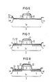
- FIG. 6 All process steps in Figure 1 except for the last are also carried out here. Since the peripheral region (P) does not have a "stacked capacitor", no "buried contact” (BC) is required and the Teos (tetraethylorthosilicate), nitride or Teos / nitride layer (TS1) forms a closed surface over the peripheral area (P).
- BC buried contact
- Teos tetraethylorthosilicate
- nitride or Teos / nitride layer (TS1) forms a closed surface over the peripheral area (P).
- the method steps correspond to those in FIG. 2 with the following exceptions. Since there is no varactor in the peripheral region (P), the doped polysilicon layer (P1) can be removed completely here. Instead of diffusing out the doped polysilicon layer (P1), which was used in FIG. 1 to dope the drain region (D), the source region (S) and drain region (D) are doped together by means of a doping method such as an implantation.
- FIG. 8 The process steps carried out in FIG. 8 again correspond to those in FIG. 3, but the doped polysilicon layer (P2) for the varactor is used, as are the teos (tetraethyl orthosilicate), nitride or teos / nitride layer (TS1) and the dielectric layer (D1). removed in the area of the source (S) and drain area (D).
- P2 doped polysilicon layer
- This layer prevents oxidation of the source-drain diffusion region (S, D) in the connection contacts (K) during the oxidation to isolate the flanks of the polysilicon layer (P2) in FIG. 5.
- connection contacts (K) of the source (S) and drain area (D) in the periphery (P) are etched away and finally the connection contacts (K) are metallized.
Landscapes
- Engineering & Computer Science (AREA)
- Manufacturing & Machinery (AREA)
- Semiconductor Memories (AREA)
- Semiconductor Integrated Circuits (AREA)
Priority Applications (1)
| Application Number | Priority Date | Filing Date | Title |
|---|---|---|---|
| AT87111193T ATE79202T1 (de) | 1986-08-22 | 1987-08-03 | Transistorvaraktoranordnung fuer dynamische halbleiterspeicher. |
Applications Claiming Priority (2)
| Application Number | Priority Date | Filing Date | Title |
|---|---|---|---|
| DE3628500 | 1986-08-22 | ||
| DE3628500 | 1986-08-22 |
Publications (2)
| Publication Number | Publication Date |
|---|---|
| EP0258657A1 true EP0258657A1 (fr) | 1988-03-09 |
| EP0258657B1 EP0258657B1 (fr) | 1992-08-05 |
Family
ID=6307933
Family Applications (1)
| Application Number | Title | Priority Date | Filing Date |
|---|---|---|---|
| EP87111193A Expired - Lifetime EP0258657B1 (fr) | 1986-08-22 | 1987-08-03 | Dispositif transistor-varactor pour mémoire dynamique à semi-conducteur |
Country Status (7)
| Country | Link |
|---|---|
| US (1) | US4855801A (fr) |
| EP (1) | EP0258657B1 (fr) |
| JP (1) | JP2628494B2 (fr) |
| KR (1) | KR920005702B1 (fr) |
| AT (1) | ATE79202T1 (fr) |
| DE (1) | DE3780885D1 (fr) |
| HK (1) | HK8895A (fr) |
Cited By (11)
| Publication number | Priority date | Publication date | Assignee | Title |
|---|---|---|---|---|
| DE3842474A1 (de) * | 1988-06-07 | 1989-12-14 | Samsung Electronics Co Ltd | Stapelkondensator-dram und verfahren zur herstellung derselben |
| EP0386947A3 (fr) * | 1989-03-06 | 1991-02-13 | STMicroelectronics, Inc. | Cellule de mémoire dynamique à access aléatoire |
| EP0443439A3 (en) * | 1990-02-23 | 1991-10-02 | Institut Fur Halbleiterphysik | One-transistor-storage cell device and method for making the same |
| GB2242782A (en) * | 1990-04-04 | 1991-10-09 | Gold Star Electronics | Process and structure for a transistor-capacitor cell |
| EP0401113A3 (fr) * | 1989-05-31 | 1992-07-29 | Fujitsu Limited | Dispositif semi-conducteur et son procédé de fabrication |
| DE4203565A1 (de) * | 1991-02-08 | 1992-08-13 | Mitsubishi Electric Corp | Dram und verfahren zu dessen herstellung |
| EP0512463A1 (fr) * | 1991-05-03 | 1992-11-11 | Micron Technology, Inc. | Procédé de fabrication des mémoires dynamiques à accès aléatoire |
| US5272103A (en) * | 1991-02-08 | 1993-12-21 | Mitsubishi Denki Kabushiki Kaisha | DRAM having a large dielectric breakdown voltage between an adjacent conductive layer and a capacitor electrode and method of manufacture thereof |
| US5286998A (en) * | 1989-05-31 | 1994-02-15 | Fujitsu Limited | Semiconductor device having two transistors forming a memory cell and a peripheral circuit, wherein the impurity region of the first transistor is not subjected to an etching atmosphere |
| DE4330471C1 (de) * | 1993-09-08 | 1994-10-20 | Siemens Ag | Herstellverfahren für ein Bitleitungskontaktloch einer Speicherzelle |
| GB2294807A (en) * | 1994-11-02 | 1996-05-08 | Mosel Vitelic Inc | Self-registered capacitor bottom plate local interconnect scheme for DRAM |
Families Citing this family (34)
| Publication number | Priority date | Publication date | Assignee | Title |
|---|---|---|---|---|
| JPH0789569B2 (ja) * | 1986-03-26 | 1995-09-27 | 株式会社日立製作所 | 半導体集積回路装置及びその製造方法 |
| US5191402A (en) * | 1986-10-27 | 1993-03-02 | Seiko Epson Corporation | Semiconductor device having an inter-layer insulating film disposed between two wiring layers |
| US5612557A (en) * | 1986-10-27 | 1997-03-18 | Seiko Epson Corporation | Semiconductor device having an inter-layer insulating film disposed between two wiring layers |
| JP2602219B2 (ja) * | 1987-02-06 | 1997-04-23 | 株式会社日立製作所 | 半導体記憶装置 |
| KR920007787B1 (ko) * | 1987-06-09 | 1992-09-17 | 세이꼬 엡슨 가부시끼가이샤 | 반도체 장치 및 그 제조방법 |
| DE3856143T2 (de) * | 1987-06-17 | 1998-10-29 | Fujitsu Ltd | Verfahren zum Herstellen einer dynamischen Speicherzelle mit wahlfreiem Zugriff |
| US5650647A (en) * | 1987-06-17 | 1997-07-22 | Fujitsu Limited | Dynamic random access memory device and method of producing same |
| KR100212098B1 (ko) * | 1987-09-19 | 1999-08-02 | 가나이 쓰도무 | 반도체 집적회로 장치 및 그 제조 방법과 반도체 집적 회로 장치의 배선기판 및 그 제조 방법 |
| JPH0828427B2 (ja) * | 1988-09-14 | 1996-03-21 | 三菱電機株式会社 | 半導体装置およびその製造方法 |
| JP2633650B2 (ja) * | 1988-09-30 | 1997-07-23 | 株式会社東芝 | 半導体記憶装置およびその製造方法 |
| JP2904533B2 (ja) * | 1989-03-09 | 1999-06-14 | 株式会社東芝 | 半導体装置の製造方法 |
| US5162249A (en) * | 1989-04-03 | 1992-11-10 | Hyundai Electronics Industries Co., Ltd. | Method of making semiconductor memory device having a double stacked capacitor |
| NL8900989A (nl) * | 1989-04-20 | 1990-11-16 | Philips Nv | Halfgeleiderinrichting met een in een kunststof omhulling ingebed halfgeleiderlichaam. |
| KR940005729B1 (ko) * | 1989-06-13 | 1994-06-23 | 삼성전자 주식회사 | 디램셀의 제조방법 및 구조 |
| JPH06105726B2 (ja) * | 1989-10-13 | 1994-12-21 | 三菱電機株式会社 | 半導体集積回路装置 |
| US5116776A (en) * | 1989-11-30 | 1992-05-26 | Sgs-Thomson Microelectronics, Inc. | Method of making a stacked copacitor for dram cell |
| US5006481A (en) * | 1989-11-30 | 1991-04-09 | Sgs-Thomson Microelectronics, Inc. | Method of making a stacked capacitor DRAM cell |
| US5037772A (en) * | 1989-12-13 | 1991-08-06 | Texas Instruments Incorporated | Method for forming a polysilicon to polysilicon capacitor |
| US5290729A (en) * | 1990-02-16 | 1994-03-01 | Mitsubishi Denki Kabushiki Kaisha | Stacked type capacitor having a dielectric film formed on a rough surface of an electrode and method of manufacturing thereof |
| US5229314A (en) * | 1990-05-01 | 1993-07-20 | Mitsubishi Denki Kabushiki Kaisha | Method of manufacturing field effect transistor having a multilayer interconnection layer therein with tapered sidewall insulation |
| KR960006880B1 (ko) * | 1990-05-24 | 1996-05-23 | 가부시키가이샤 도시바 | 반도체 기억장치 |
| KR950008385B1 (ko) * | 1990-05-24 | 1995-07-28 | 삼성전자주식회사 | 반도체 소자의 워드라인 형성방법 |
| US5061646A (en) * | 1990-06-29 | 1991-10-29 | Motorola, Inc. | Method for forming a self-aligned bipolar transistor |
| EP0469555B1 (fr) * | 1990-07-31 | 1996-04-17 | Nec Corporation | Electrode à stockage de charges d'une capacité et sa méthode de fabrication |
| JPH0521744A (ja) * | 1991-07-10 | 1993-01-29 | Sony Corp | 半導体記憶装置のキヤパシタおよびその製造方法 |
| US5134085A (en) * | 1991-11-21 | 1992-07-28 | Micron Technology, Inc. | Reduced-mask, split-polysilicon CMOS process, incorporating stacked-capacitor cells, for fabricating multi-megabit dynamic random access memories |
| US5525534A (en) * | 1992-03-13 | 1996-06-11 | Fujitsu Limited | Method of producing a semiconductor device using a reticle having a polygonal shaped hole |
| US5338700A (en) * | 1993-04-14 | 1994-08-16 | Micron Semiconductor, Inc. | Method of forming a bit line over capacitor array of memory cells |
| US5498562A (en) * | 1993-04-07 | 1996-03-12 | Micron Technology, Inc. | Semiconductor processing methods of forming stacked capacitors |
| US6083831A (en) * | 1996-03-26 | 2000-07-04 | Micron Technology, Inc. | Semiconductor processing method of forming a contact pedestal, of forming a storage node of a capacitor |
| US6268779B1 (en) * | 1999-03-19 | 2001-07-31 | Telefonaktiebolaget Lm Ericsson (Publ) | Integrated oscillators and tuning circuits |
| US6667539B2 (en) | 2001-11-08 | 2003-12-23 | International Business Machines Corporation | Method to increase the tuning voltage range of MOS varactors |
| US20070075364A1 (en) * | 2005-09-30 | 2007-04-05 | Analog Power Intellectual Properties Limited | Power MOSFETs and methods of making same |
| US8921977B2 (en) * | 2011-12-21 | 2014-12-30 | Nan Ya Technology Corporation | Capacitor array and method of fabricating the same |
Citations (3)
| Publication number | Priority date | Publication date | Assignee | Title |
|---|---|---|---|---|
| US4356040A (en) * | 1980-05-02 | 1982-10-26 | Texas Instruments Incorporated | Semiconductor device having improved interlevel conductor insulation |
| EP0112670A1 (fr) * | 1982-12-20 | 1984-07-04 | Fujitsu Limited | Dispositif de mémoire à semi-conducteurs pourvu de cellules de mémoire à capacité empilées |
| EP0161850A1 (fr) * | 1984-04-28 | 1985-11-21 | Fujitsu Limited | Dispositif de mémoire à semi-conducteurs ayant des cellules-mémoires à capacité empilée et méthode de fabrication |
Family Cites Families (4)
| Publication number | Priority date | Publication date | Assignee | Title |
|---|---|---|---|---|
| US4649406A (en) * | 1982-12-20 | 1987-03-10 | Fujitsu Limited | Semiconductor memory device having stacked capacitor-type memory cells |
| JPS6055637B2 (ja) * | 1983-06-14 | 1985-12-05 | 東洋リノリユ−ム株式会社 | 床材の裏面処理方法 |
| JPS616858A (ja) * | 1984-06-20 | 1986-01-13 | Matsushita Electric Ind Co Ltd | 半導体記憶装置およびその製造方法 |
| JPS61123181A (ja) * | 1984-11-15 | 1986-06-11 | Fujitsu Ltd | 半導体装置の製造方法 |
-
1987
- 1987-07-16 US US07/074,334 patent/US4855801A/en not_active Expired - Lifetime
- 1987-08-03 AT AT87111193T patent/ATE79202T1/de not_active IP Right Cessation
- 1987-08-03 DE DE8787111193T patent/DE3780885D1/de not_active Expired - Lifetime
- 1987-08-03 EP EP87111193A patent/EP0258657B1/fr not_active Expired - Lifetime
- 1987-08-21 JP JP62209113A patent/JP2628494B2/ja not_active Expired - Lifetime
- 1987-08-22 KR KR1019870009231A patent/KR920005702B1/ko not_active Expired
-
1995
- 1995-01-19 HK HK8895A patent/HK8895A/xx not_active IP Right Cessation
Patent Citations (4)
| Publication number | Priority date | Publication date | Assignee | Title |
|---|---|---|---|---|
| US4356040A (en) * | 1980-05-02 | 1982-10-26 | Texas Instruments Incorporated | Semiconductor device having improved interlevel conductor insulation |
| US4356040B1 (fr) * | 1980-05-02 | 1991-12-10 | Texas Instruments Inc | |
| EP0112670A1 (fr) * | 1982-12-20 | 1984-07-04 | Fujitsu Limited | Dispositif de mémoire à semi-conducteurs pourvu de cellules de mémoire à capacité empilées |
| EP0161850A1 (fr) * | 1984-04-28 | 1985-11-21 | Fujitsu Limited | Dispositif de mémoire à semi-conducteurs ayant des cellules-mémoires à capacité empilée et méthode de fabrication |
Non-Patent Citations (1)
| Title |
|---|
| IEEE TRANSACTIONS ON ELECTRON DEVICES, Band ED-29, Nr. 3, März 1982, Seiten 368-376, New York, US; K. OHTA et al.: "Quadruply self-aligned stacked high-capacitance RAM using Ta2O5 high-density VLSI dynamic memory" * |
Cited By (13)
| Publication number | Priority date | Publication date | Assignee | Title |
|---|---|---|---|---|
| DE3842474A1 (de) * | 1988-06-07 | 1989-12-14 | Samsung Electronics Co Ltd | Stapelkondensator-dram und verfahren zur herstellung derselben |
| EP0386947A3 (fr) * | 1989-03-06 | 1991-02-13 | STMicroelectronics, Inc. | Cellule de mémoire dynamique à access aléatoire |
| US5286998A (en) * | 1989-05-31 | 1994-02-15 | Fujitsu Limited | Semiconductor device having two transistors forming a memory cell and a peripheral circuit, wherein the impurity region of the first transistor is not subjected to an etching atmosphere |
| EP0401113A3 (fr) * | 1989-05-31 | 1992-07-29 | Fujitsu Limited | Dispositif semi-conducteur et son procédé de fabrication |
| EP0443439A3 (en) * | 1990-02-23 | 1991-10-02 | Institut Fur Halbleiterphysik | One-transistor-storage cell device and method for making the same |
| GB2242782B (en) * | 1990-04-04 | 1994-02-16 | Gold Star Electronics | Process and structure for a transistor-capacitor cell |
| GB2242782A (en) * | 1990-04-04 | 1991-10-09 | Gold Star Electronics | Process and structure for a transistor-capacitor cell |
| US5272103A (en) * | 1991-02-08 | 1993-12-21 | Mitsubishi Denki Kabushiki Kaisha | DRAM having a large dielectric breakdown voltage between an adjacent conductive layer and a capacitor electrode and method of manufacture thereof |
| DE4203565A1 (de) * | 1991-02-08 | 1992-08-13 | Mitsubishi Electric Corp | Dram und verfahren zu dessen herstellung |
| EP0512463A1 (fr) * | 1991-05-03 | 1992-11-11 | Micron Technology, Inc. | Procédé de fabrication des mémoires dynamiques à accès aléatoire |
| DE4330471C1 (de) * | 1993-09-08 | 1994-10-20 | Siemens Ag | Herstellverfahren für ein Bitleitungskontaktloch einer Speicherzelle |
| GB2294807A (en) * | 1994-11-02 | 1996-05-08 | Mosel Vitelic Inc | Self-registered capacitor bottom plate local interconnect scheme for DRAM |
| GB2294807B (en) * | 1994-11-02 | 1998-10-21 | Mosel Vitelic Inc | Self-registered capacitor bottom plate local interconnect scheme for dram |
Also Published As
| Publication number | Publication date |
|---|---|
| ATE79202T1 (de) | 1992-08-15 |
| JP2628494B2 (ja) | 1997-07-09 |
| US4855801A (en) | 1989-08-08 |
| EP0258657B1 (fr) | 1992-08-05 |
| KR920005702B1 (ko) | 1992-07-13 |
| DE3780885D1 (de) | 1992-09-10 |
| HK8895A (en) | 1995-01-27 |
| KR880003429A (ko) | 1988-05-17 |
| JPS6373553A (ja) | 1988-04-04 |
Similar Documents
| Publication | Publication Date | Title |
|---|---|---|
| EP0258657B1 (fr) | Dispositif transistor-varactor pour mémoire dynamique à semi-conducteur | |
| DE4332074C2 (de) | Halbleiterspeichereinrichtung und Verfahren zu ihrer Herstellung | |
| DE4408764C2 (de) | Halbleiterspeicheranordnung | |
| EP0744771B1 (fr) | Procédé de fabrication d'une cellule de stockage DRAM avec transistor vertical | |
| DE4127967C2 (de) | MOS-Transistor mit Gate-Drain-Elektrodenüberlapp und Verfahren zu seiner Herstellung | |
| DE4028488C2 (de) | Verfahren zur Herstellung einer Halbleiterspeichervorrichtung | |
| DE4007582C2 (de) | Verfahren zum Herstellen von mindestens zwei Kontakten in einem Halbleiterbauelement | |
| DE4142961A1 (de) | Dram-speicheranordnung | |
| DE4301690A1 (fr) | ||
| EP0744772A1 (fr) | Cellule de stockage DRAM à transistor vertical et son procédé de fabrication | |
| DE10324491A1 (de) | Herstellungsverfahren für Dual-Workfunction-Logikbauelemente in vertikalen DRAM-Prozessen | |
| DE3785317T2 (de) | Matrix hoher Packungsdichte aus dynamischen VMOS RAM. | |
| EP0282629B1 (fr) | Structure tridimensionnelle de cellule de mémoire semi-conductrice dynamique à condensateur sillonné et procédé de fabrication d'un contact pour la ligne de bit | |
| DE69609224T2 (de) | Kondensator für eine integrierte Schaltung mit leitendem Graben | |
| EP0875937A2 (fr) | Réseau de cellules DRAM et son procédé de fabrication | |
| DE3931711A1 (de) | Dynamische random-access-speicherzelle und verfahren zur herstellung | |
| DE4327813C2 (de) | Verfahren zur Herstellung eines DRAM's | |
| DE2921010A1 (de) | Verfahren zur herstellung von sowie strukturen fuer vlsi-schaltungen mit hoher dichte | |
| DE4109299C2 (de) | Halbleiterspeichereinrichtung und Herstellungsverfahren hierfür | |
| DE10109564A1 (de) | Grabenkondensator und Verfahren zu seiner Herstellung | |
| DE10012198B4 (de) | Zylindrisches Kondensatorbauelement mit innenseitigem HSG-Silicium und Verfahren zu seiner Herstellung | |
| DE4130890A1 (de) | Verfahren zur herstellung eines kondensators unter verwendung des feldeffekttransistor-prozesses und mit hilfe des verfahrens hergestellte struktur | |
| EP0925607B1 (fr) | Procede de production d'une matrice cellulaire a dram | |
| DE4135178A1 (de) | Dram-speicheranordnung | |
| EP0263941B1 (fr) | Configuration de cellules de mémoire pour mémoires dynamiques semi-conductrices |
Legal Events
| Date | Code | Title | Description |
|---|---|---|---|
| PUAI | Public reference made under article 153(3) epc to a published international application that has entered the european phase |
Free format text: ORIGINAL CODE: 0009012 |
|
| AK | Designated contracting states |
Kind code of ref document: A1 Designated state(s): AT DE FR GB IT NL |
|
| 17P | Request for examination filed |
Effective date: 19880506 |
|
| 17Q | First examination report despatched |
Effective date: 19910207 |
|
| GRAA | (expected) grant |
Free format text: ORIGINAL CODE: 0009210 |
|
| AK | Designated contracting states |
Kind code of ref document: B1 Designated state(s): AT DE FR GB IT NL |
|
| REF | Corresponds to: |
Ref document number: 79202 Country of ref document: AT Date of ref document: 19920815 Kind code of ref document: T |
|
| REF | Corresponds to: |
Ref document number: 3780885 Country of ref document: DE Date of ref document: 19920910 |
|
| ET | Fr: translation filed | ||
| ITF | It: translation for a ep patent filed | ||
| GBT | Gb: translation of ep patent filed (gb section 77(6)(a)/1977) | ||
| PLBE | No opposition filed within time limit |
Free format text: ORIGINAL CODE: 0009261 |
|
| STAA | Information on the status of an ep patent application or granted ep patent |
Free format text: STATUS: NO OPPOSITION FILED WITHIN TIME LIMIT |
|
| 26N | No opposition filed | ||
| PGFP | Annual fee paid to national office [announced via postgrant information from national office to epo] |
Ref country code: AT Payment date: 19960724 Year of fee payment: 10 |
|
| PGFP | Annual fee paid to national office [announced via postgrant information from national office to epo] |
Ref country code: NL Payment date: 19960821 Year of fee payment: 10 |
|
| PG25 | Lapsed in a contracting state [announced via postgrant information from national office to epo] |
Ref country code: AT Free format text: LAPSE BECAUSE OF NON-PAYMENT OF DUE FEES Effective date: 19970803 |
|
| PG25 | Lapsed in a contracting state [announced via postgrant information from national office to epo] |
Ref country code: NL Free format text: LAPSE BECAUSE OF NON-PAYMENT OF DUE FEES Effective date: 19980301 |
|
| NLV4 | Nl: lapsed or anulled due to non-payment of the annual fee |
Effective date: 19980301 |
|
| REG | Reference to a national code |
Ref country code: GB Ref legal event code: IF02 |
|
| PGFP | Annual fee paid to national office [announced via postgrant information from national office to epo] |
Ref country code: GB Payment date: 20050725 Year of fee payment: 19 |
|
| PGFP | Annual fee paid to national office [announced via postgrant information from national office to epo] |
Ref country code: FR Payment date: 20060817 Year of fee payment: 20 |
|
| PGFP | Annual fee paid to national office [announced via postgrant information from national office to epo] |
Ref country code: IT Payment date: 20060831 Year of fee payment: 20 |
|
| PGFP | Annual fee paid to national office [announced via postgrant information from national office to epo] |
Ref country code: DE Payment date: 20061017 Year of fee payment: 20 |
|
| GBPC | Gb: european patent ceased through non-payment of renewal fee |
Effective date: 20060803 |
|
| PG25 | Lapsed in a contracting state [announced via postgrant information from national office to epo] |
Ref country code: GB Free format text: LAPSE BECAUSE OF NON-PAYMENT OF DUE FEES Effective date: 20060803 |