EP0262610A2 - Dispositif de commutation ayant un gaz d'électrons à deux dimensions - Google Patents
Dispositif de commutation ayant un gaz d'électrons à deux dimensions Download PDFInfo
- Publication number
- EP0262610A2 EP0262610A2 EP87114045A EP87114045A EP0262610A2 EP 0262610 A2 EP0262610 A2 EP 0262610A2 EP 87114045 A EP87114045 A EP 87114045A EP 87114045 A EP87114045 A EP 87114045A EP 0262610 A2 EP0262610 A2 EP 0262610A2
- Authority
- EP
- European Patent Office
- Prior art keywords
- drain
- source
- charge carriers
- channel
- field effect
- Prior art date
- Legal status (The legal status is an assumption and is not a legal conclusion. Google has not performed a legal analysis and makes no representation as to the accuracy of the status listed.)
- Withdrawn
Links
Images

Classifications
-
- H—ELECTRICITY
- H10—SEMICONDUCTOR DEVICES; ELECTRIC SOLID-STATE DEVICES NOT OTHERWISE PROVIDED FOR
- H10D—INORGANIC ELECTRIC SEMICONDUCTOR DEVICES
- H10D62/00—Semiconductor bodies, or regions thereof, of devices having potential barriers
- H10D62/10—Shapes, relative sizes or dispositions of the regions of the semiconductor bodies; Shapes of the semiconductor bodies
- H10D62/17—Semiconductor regions connected to electrodes not carrying current to be rectified, amplified or switched, e.g. channel regions
- H10D62/213—Channel regions of field-effect devices
- H10D62/221—Channel regions of field-effect devices of FETs
-
- H—ELECTRICITY
- H10—SEMICONDUCTOR DEVICES; ELECTRIC SOLID-STATE DEVICES NOT OTHERWISE PROVIDED FOR
- H10D—INORGANIC ELECTRIC SEMICONDUCTOR DEVICES
- H10D30/00—Field-effect transistors [FET]
- H10D30/40—FETs having zero-dimensional [0D], one-dimensional [1D] or two-dimensional [2D] charge carrier gas channels
- H10D30/47—FETs having zero-dimensional [0D], one-dimensional [1D] or two-dimensional [2D] charge carrier gas channels having two-dimensional [2D] charge carrier gas channels, e.g. nanoribbon FETs or high electron mobility transistors [HEMT]
- H10D30/471—High electron mobility transistors [HEMT] or high hole mobility transistors [HHMT]
- H10D30/473—High electron mobility transistors [HEMT] or high hole mobility transistors [HHMT] having confinement of carriers by multiple heterojunctions, e.g. quantum well HEMT
- H10D30/4732—High electron mobility transistors [HEMT] or high hole mobility transistors [HHMT] having confinement of carriers by multiple heterojunctions, e.g. quantum well HEMT using Group III-V semiconductor material
-
- H—ELECTRICITY
- H10—SEMICONDUCTOR DEVICES; ELECTRIC SOLID-STATE DEVICES NOT OTHERWISE PROVIDED FOR
- H10D—INORGANIC ELECTRIC SEMICONDUCTOR DEVICES
- H10D30/00—Field-effect transistors [FET]
- H10D30/40—FETs having zero-dimensional [0D], one-dimensional [1D] or two-dimensional [2D] charge carrier gas channels
- H10D30/47—FETs having zero-dimensional [0D], one-dimensional [1D] or two-dimensional [2D] charge carrier gas channels having two-dimensional [2D] charge carrier gas channels, e.g. nanoribbon FETs or high electron mobility transistors [HEMT]
- H10D30/471—High electron mobility transistors [HEMT] or high hole mobility transistors [HHMT]
- H10D30/474—High electron mobility transistors [HEMT] or high hole mobility transistors [HHMT] having multiple parallel 2D charge carrier gas channels
Definitions
- the present invention relates to a switching logic device in the form of a field effect transistor configuration. More particularly, this invention relates to a double heterojunction structure in a logic device providing an upper conduction channel and a lower conduction channel each capable of producing and confining a quasi-two-dimensional electron gas (2 DEG).
- switching on is produced by moving a 2 DEG from one channel to the other channel to provide channel alignment completing conduction between source and drain terminals of the device.
- Switching off also involves moving a 2 DEG between channels but to produce misalignment preventing or disrupting conduction between source and drain terminals of the device.
- FETs field effect transistors
- Another advantage of the FET is their relatively simple structure for ease of fabrication processing.
- the fundamental operation of conventional FETs involves modulating the density of charge carriers traversing conduction channels in a semiconductor medium extending between source and drain electrodes in response to a signal potential applied to one or more gate electrodes.
- the gate electrode controls the electrical conductivity between the source and drain electrode.
- a limiting factor in the high speed performance of most conventional FET devices is determined by the channel transit time of the charge carriers take in traveling the length of the conduction path spanning between the drain and source electrodes.
- the channel transit time is directly proportional to the channel length and inversely proportional to the carrier velocity.
- the minimum achievable channel transit time is on the order or one picosecond (10 ⁇ 12 second) with minimum channel length and fastest carrier velocity.
- Typical high speed devices of this type are known as gallium arsenide Schottky field effect transistors.
- An object of the present invention is to control selectively the formation of one or more electron gases in a double heterojunction or double quantum well device structure to achieve extremely high speed switching operation.
- the invention takes the form of a double heterojunction semiconductor device wherein control in the establishment of a quasi-two-dimensional electron gas at one location via a gate terminal between two possible locations is used to complete or prevent the formation of a continuous conduction channel from a first terminal to another terminal of the device.
- a FET device configuration includes a channel capable of supporting two-electron gases at two different locations wherein the formation of an electron gas in a predetermined portion of the channel is allowed to occur at only a selected one of the two different locations.
- the corresponding portion of the device assumes an on-state.
- the conduction path is not complete between the two associated terminals so that the associated portion of the device assumes an off-state.
- changing the polarity of the electrical field oriented normal with respect to the longitudinal orientation of the channel shifts the formation of two possible electron gases at each of the two heterojunction interfaces to only one or the other location for a single electron gas at one heterojunction interface thereby completing or interrupting the conduction path between source and drain terminals of the device to provide high speeding switching operation.
- Either two (paired) drain electrodes or two (paired) source electrodes provide a device configuration wherein the selected portion of the channel abutting the associated zone or paired electrodes is arranged to support only one electron gas in a predetermined location.
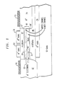
- Fig. 1 is a cross-sectional view of a channel portion of an illustrative device for demonstrating the fundamental operational principles of the invention.
- the various device structures such as Fig. 1 and other figures are illustrated in enlarged versions which are also not in correct proportions for the purpose of clearly illustrating the structure. For example, very thin layers are depicted with exaggerated thickness.
- the basic structure of the device of Fig. 1 corresponds to a field effect transistor (FET) including source contact 11 for providing, in this case, a source of electon charge carriers from source zone 12.
- FET field effect transistor
- Source zone 11 under appropriate biasing with respect to drain contact 13 and associated drain zone 14 emits electrons into channel zone 16 bounded on its upper and lower regions by upper zone 17 and a lower zone 18 to form an upper interface and a lower interface channel structure.
- channel zone 16 is divided into upper and lower channels by dotted line 19.
- dotted line 19 indicates the formation of two separate channels (upper and lower) within zone 16.
- zones 17 and 18 possess a higher conduction band energy than the intermediate material of channel zone 16.
- a suitable material is Al x Ga 1-x As for zones 17 and 18. Since zones 17 and 18 have the same composition, the two electron gases providing conduction channels are formed of charge carriers exhibiting the same mobility at the two equivalent heterojunction interfaces of n-AlGaAs and the relatively high purity (undoped) GaAs material of channel zone 16. It should be understood that different combinations of materials may also be used to provide the dual heterojunction structure.
- At least one electric field is established normal to the longitudinal axis and orientation of the zone.
- a first gate electrode 22 is placed along side of a second gate electrode 23 for establishing normal electric fields with respect to common gate electrode 24.
- gate (back) electrode 24 is not necessarily essential and the same or equivalent operation will occur in its absence.
- an electric field established between gate electrode 22 and common gate electrode 24 has the ability to favor only one of the two possible interfaces for the formation and containment of a single electron gas of charge carriers.
- the electron gas depending upon the polarity of the electric field may favor formation at either the upper interface 20 or the lower interface 21.
- a second electric field established between second gate electrode 23 and common electrode 24 will have a corresponding effect in that portion of zone 16 passing through this electric field.
- Switching of the device of Fig. 1 to the on-state is accomplished by aligning the two independent electron gases to form a complete conduction channel. Conversely by displacing the two electron gases from each other to lie at the opposite interfaces of zone 16 thereby interrupting the conduction path between source 11 and drain 13 switches the device of Fig. 1 to the off-state. Since this mechanism of switching between the two possible locations of the electron gas is independent of the carrier transit time consumed in propagating the length of zone 16, extremely high speed switching will result in the utilization of this principle.
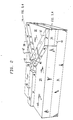
- Fig. 2 is a perspective illustration of a branching device in accordance with the invention.
- a suitable material for substrate 31 is gallium arsenide (GaAs).
- Triangular region 32 and rhombic shaped regions 33 and 34 are semi-insulating and play no role in the active device structure other than to define the geometry of a Y-shaped active channel region having its base under common contact and terminal 36 with one branch portion extending under terminal 37 and the other branch portion extending under terminal 38.
- Under terminals 36 and 37 are two contacted zones, one zone 39 of which is shown extending to the edge of the device of Fig. 2 under contact/terminal 37.
- zone 41 is used to provide isolation for zone 39. It should be understood that zones 39 and 41 may be though of as respectively corresponding to zones 14 and 18 as depicted in Fig. 1 when terminal 37 is a drain terminal. When terminal 37 is one of two source terminals, then terminal 37 generally corresponds to source terminal 11.
- the principle of establishing or interrupting a current path between the common source 11 and drain 13 of Fig. 1 by aligning or misaligning the conductive two-dimensional electron gas in either the upper or lower interface of the channel region 16 may be used to switch the current path between common terminal 36 and terminal 37 to a different path between terminal 36 and another terminal 38 as shown in Fig. 2.
- the conductive two-dimensional electron gas resides in the upper or lower interface of the channel areas under the respective gates.
- the conductive path is established only between the common terminal 36 and either terminal 37 or terminal 38 depending upon the voltage applied to gate 44 and thus the two-dimensional electron gas resides in a position (upper or lower interface of the branching channel region) in the area under gate 44.
- the current path may be switched from terminal 36 to terminal 37 or to terminal 36 to terminal 38. Such switching is accomplished only by one gate voltage change applied to gate 44 shifting the two dimensional electron gas from the lower to the upper interface of the channel 16 or vice versa.
- one application of the switching mechanism may be used to switch on and off a conduction channel between two terminals of device.
- Another application of the switching mechanism may be used to steer or branch a conduction channel extending from a common terminal to a selected one of two other terminals on the device. In other words instead of switching between on and off states, the device switches a current path terminated at a common terminal between two other terminals.
- This application is equivalent in basic structure and operation to a very fast acting single pole double throw switch.
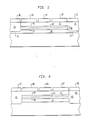
- Fig. 3 provides a first cross-sectional view of the internal structure of Fig. 2 take along the indicated V-shaped axis.
- Fig. 3 illustrates the internal zone structure wherein a source terminal (not shown in Fig.3) serves as the common terminal between two channel terminals.
- Selector terminal 44 determines whether the 2-DEG is located at interface 49 or 50 for the electrons being injected into drain zone 51 by the common source zone.
- selector terminal 46 is biased at a first potential and polarity to favour one interface location for its localized 2-DEG while selector terminal 47 is biased at another potential and polarity to favor the other interface location for its associated 2-DEG while selector terminal 47 is biased at another potential and polarity to favor the other interface location for its associated 2-DEG.
- Fig. 3 is symmetrical about its middle and that drain zone 39 and 40 have the same dimensions and doping levels. Spacing regions 41 and 42 serve to provide isolation for their corresponding drain zones.
- Fig. 4 provides a cross-sectional view of an alternative structure for the branching device of Fig. 2.
- the common terminal (not shown in Fig. 4) is the drain associated with either one of two source terminals.
- Respectively, associated with each of two source terminals 57 and 58 are source zones 59 and 60.
- Fig. 4 is symmetrical about its middle region similar to Fig. 3.
- the same principles are used to provide alignment or displacement between the associated 2-DEGs of selector 64 and selectors 66 and 67. Therefore, the current branching now occurs between a common drain and the two source terminals 57 and 58.
- a double heterostructure is provided for the formation of 2-DEGs at either interface 61 or 62 which are also the upper and lower boundaries of bounding channel zone 73.
- n+GaAs may be used or a contact of suitable metal may be used.
- n+GaAs contact material no offset voltage will develop in the drain current versus selector or gate voltage along the voltage axis.
- a voltage offset typically of about 0.8 volts will develop due to the difference in work function introduced by the metal-semiconductor contact interface.
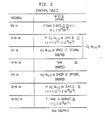
- Fig. 5 presents structural information (Structural Table I) providing suitable thicknesses, material, and doping or concentration levels for the various elements depicted in Fig 1.
- the table of Fig. 5 is arranged vertically to generally correspond to the arrangement of Fig. 1.
- the layer thickness dimensions are quite thin and listed in nanometers (nm) units for the epitaxial layers.
- Fig. 5 is a structural version wherein the Al x Ga 1-x As layers are undoped.
- Fig. 6 depicts in structural table II the parameters for a device arrangement wherein the layers are doped with Al x Ga 1-x As.
- Fig. 7 illustrates structural table III which is only directed to channel zone portion applicable to both structural tables I and II wherein an optical barrier layer such as 19 in the middle of channel zone 16 provides a dual quantum well profile for a device in accordance with the principles of the invention.
- an optional barrier layer may be utilized at the location of dashed line 52 in Fig. 3 and the location of dashed line 64 in Fig. 4. This optional barrier serves to improve the separation of the two 2-DEG positions in the channel for the purpose of increasing the sharpness in the electrical switching characteristic of the device.
- the channel region and/or the barrier may also be doped using different dopants and concentrations at different locations to provide desirable dopant gradients vertically to achieve performance advantages.
- backgate 24 may be omitted in situations advantageous to the processing sequence used in the device fabrication.
- the n+-GaAS material for the gate electrodes metal may be used (e.g.,TiPtAu).
Landscapes
- Junction Field-Effect Transistors (AREA)
Applications Claiming Priority (2)
| Application Number | Priority Date | Filing Date | Title |
|---|---|---|---|
| US91304986A | 1986-09-29 | 1986-09-29 | |
| US913049 | 1986-09-29 |
Publications (2)
| Publication Number | Publication Date |
|---|---|
| EP0262610A2 true EP0262610A2 (fr) | 1988-04-06 |
| EP0262610A3 EP0262610A3 (fr) | 1989-02-15 |
Family
ID=25432886
Family Applications (1)
| Application Number | Title | Priority Date | Filing Date |
|---|---|---|---|
| EP87114045A Withdrawn EP0262610A3 (fr) | 1986-09-29 | 1987-09-25 | Dispositif de commutation ayant un gaz d'électrons à deux dimensions |
Country Status (2)
| Country | Link |
|---|---|
| EP (1) | EP0262610A3 (fr) |
| JP (1) | JPS63102374A (fr) |
Cited By (3)
| Publication number | Priority date | Publication date | Assignee | Title |
|---|---|---|---|---|
| EP0336172A3 (fr) * | 1988-04-08 | 1991-05-08 | Siemens Aktiengesellschaft | Dispositif à semiconducteur, utilisable comme commutateur extrêmement rapide |
| GB2284929A (en) * | 1993-12-14 | 1995-06-21 | Toshiba Cambridge Res Center | High electron mobility transistors |
| CN110828565A (zh) * | 2019-10-30 | 2020-02-21 | 杭州电子科技大学 | 一种具有p型埋层的双沟道高耐压氮化镓场效应晶体管 |
Family Cites Families (6)
| Publication number | Priority date | Publication date | Assignee | Title |
|---|---|---|---|---|
| DE2804165C2 (de) * | 1978-02-01 | 1982-11-11 | Licentia Patent-Verwaltungs-Gmbh, 6000 Frankfurt | Halbleiteranordnung mit einem für die Stromführung geeigneten Kanal und Verfahren zum Betrieb dieser Halbleiteranordnung |
| JPS58178572A (ja) * | 1982-04-14 | 1983-10-19 | Hiroyuki Sakaki | 移動度変調形電界効果トランジスタ |
| JPS5931071A (ja) * | 1982-08-13 | 1984-02-18 | Oki Electric Ind Co Ltd | 電界効果トランジスタ |
| US4558337A (en) * | 1984-05-30 | 1985-12-10 | Texas Instruments Inc. | Multiple high electron mobility transistor structures without inverted heterojunctions |
| DE3432901C1 (de) * | 1984-09-07 | 1986-01-16 | Licentia Patent-Verwaltungs-Gmbh, 6000 Frankfurt | Halbleiteranordnung |
| JPS61174776A (ja) * | 1985-01-30 | 1986-08-06 | Sony Corp | ヘテロ接合電界効果トランジスタ |
-
1987
- 1987-09-24 JP JP62242405A patent/JPS63102374A/ja active Pending
- 1987-09-25 EP EP87114045A patent/EP0262610A3/fr not_active Withdrawn
Cited By (5)
| Publication number | Priority date | Publication date | Assignee | Title |
|---|---|---|---|---|
| EP0336172A3 (fr) * | 1988-04-08 | 1991-05-08 | Siemens Aktiengesellschaft | Dispositif à semiconducteur, utilisable comme commutateur extrêmement rapide |
| GB2284929A (en) * | 1993-12-14 | 1995-06-21 | Toshiba Cambridge Res Center | High electron mobility transistors |
| GB2284929B (en) * | 1993-12-14 | 1997-12-17 | Toshiba Cambridge Res Center | Semiconductor device |
| CN110828565A (zh) * | 2019-10-30 | 2020-02-21 | 杭州电子科技大学 | 一种具有p型埋层的双沟道高耐压氮化镓场效应晶体管 |
| CN110828565B (zh) * | 2019-10-30 | 2022-03-15 | 杭州电子科技大学 | 一种具有p型埋层的双沟道高耐压氮化镓场效应晶体管 |
Also Published As
| Publication number | Publication date |
|---|---|
| EP0262610A3 (fr) | 1989-02-15 |
| JPS63102374A (ja) | 1988-05-07 |
Similar Documents
| Publication | Publication Date | Title |
|---|---|---|
| US5825049A (en) | Resonant tunneling device with two-dimensional quantum well emitter and base layers | |
| KR940008230B1 (ko) | 헤테로 접합 전계 효과 트랜지스터 | |
| JPS58178572A (ja) | 移動度変調形電界効果トランジスタ | |
| JPS6327065A (ja) | ヘテロ接合二重チャネル半導体装置、この半導体装置を応用した電界効果トランジスタ、ならびにこの半導体装置を応用した負のコンダクタンスをもつ装置 | |
| JPH05110086A (ja) | トンネルトランジスタ | |
| US5359220A (en) | Hybrid bipolar/field-effect power transistor in group III-V material system | |
| US3263095A (en) | Heterojunction surface channel transistors | |
| EP0262610A2 (fr) | Dispositif de commutation ayant un gaz d'électrons à deux dimensions | |
| US5159421A (en) | Double channel heterostructures | |
| US4855797A (en) | Modulation doped high electron mobility transistor with n-i-p-i structure | |
| US4558243A (en) | Bidirectional power FET with shorting-channel off state | |
| US4882608A (en) | Multilayer semiconductor device having multiple paths of current flow | |
| US3273030A (en) | Majority carrier channel device using heterojunctions | |
| JPH07142706A (ja) | ヘテロ接合半導体装置の製造方法およびヘテロ接合半導体装置 | |
| US6031245A (en) | Semiconductor device | |
| Luryi | Induced base transistor | |
| JPS63202075A (ja) | 半導体デバイス | |
| JP2660001B2 (ja) | 導電変調型mosfet | |
| JPS60254657A (ja) | 半導体装置 | |
| GB2303246A (en) | Resonant tunneling semiconductor device | |
| JPH045274B2 (fr) | ||
| JPS62123771A (ja) | 電界効果型半導体装置 | |
| JP2504442B2 (ja) | 半導体素子 | |
| JPS62268165A (ja) | 電界効果トランジスタ | |
| EP0366861A1 (fr) | Transistor balistique semi-conducteur |
Legal Events
| Date | Code | Title | Description |
|---|---|---|---|
| PUAI | Public reference made under article 153(3) epc to a published international application that has entered the european phase |
Free format text: ORIGINAL CODE: 0009012 |
|
| AK | Designated contracting states |
Kind code of ref document: A2 Designated state(s): DE FR GB |
|
| PUAL | Search report despatched |
Free format text: ORIGINAL CODE: 0009013 |
|
| AK | Designated contracting states |
Kind code of ref document: A3 Designated state(s): DE FR GB |
|
| STAA | Information on the status of an ep patent application or granted ep patent |
Free format text: STATUS: THE APPLICATION IS DEEMED TO BE WITHDRAWN |
|
| 18D | Application deemed to be withdrawn |
Effective date: 19890816 |
|
| RIN1 | Information on inventor provided before grant (corrected) |
Inventor name: HOFMANN, KARL R. Inventor name: KOHN, ERHARD |