EP0280254A2 - Digitale Zeitschaltung mit einem endlichen Automaten - Google Patents
Digitale Zeitschaltung mit einem endlichen Automaten Download PDFInfo
- Publication number
- EP0280254A2 EP0280254A2 EP88102638A EP88102638A EP0280254A2 EP 0280254 A2 EP0280254 A2 EP 0280254A2 EP 88102638 A EP88102638 A EP 88102638A EP 88102638 A EP88102638 A EP 88102638A EP 0280254 A2 EP0280254 A2 EP 0280254A2
- Authority
- EP
- European Patent Office
- Prior art keywords
- pulse
- valid
- predetermined
- input signal
- time interval
- Prior art date
- Legal status (The legal status is an assumption and is not a legal conclusion. Google has not performed a legal analysis and makes no representation as to the accuracy of the status listed.)
- Withdrawn
Links
- 230000000737 periodic effect Effects 0.000 claims abstract description 13
- 238000000034 method Methods 0.000 claims description 7
- 230000003111 delayed effect Effects 0.000 abstract 1
- 230000007704 transition Effects 0.000 description 17
- 238000010586 diagram Methods 0.000 description 8
- 102100040862 Dual specificity protein kinase CLK1 Human genes 0.000 description 6
- 101000749294 Homo sapiens Dual specificity protein kinase CLK1 Proteins 0.000 description 6
- 239000002131 composite material Substances 0.000 description 5
- 238000001514 detection method Methods 0.000 description 5
- 102100040844 Dual specificity protein kinase CLK2 Human genes 0.000 description 2
- 101000749291 Homo sapiens Dual specificity protein kinase CLK2 Proteins 0.000 description 2
- 230000003466 anti-cipated effect Effects 0.000 description 1
- 230000008859 change Effects 0.000 description 1
- 230000004069 differentiation Effects 0.000 description 1
- 230000006870 function Effects 0.000 description 1
- 230000036039 immunity Effects 0.000 description 1
Images



Classifications
-
- H—ELECTRICITY
- H03—ELECTRONIC CIRCUITRY
- H03K—PULSE TECHNIQUE
- H03K5/00—Manipulating of pulses not covered by one of the other main groups of this subclass
- H03K5/19—Monitoring patterns of pulse trains
-
- H—ELECTRICITY
- H04—ELECTRIC COMMUNICATION TECHNIQUE
- H04N—PICTORIAL COMMUNICATION, e.g. TELEVISION
- H04N5/00—Details of television systems
- H04N5/04—Synchronising
- H04N5/08—Separation of synchronising signals from picture signals
- H04N5/10—Separation of line synchronising signal from frame synchronising signal or vice versa
Definitions
- the present invention relates to digital timing generation, and more particularly to digital timing generation using a state machine to identify a specific pulse pattern within an input signal from which the presence of a valid input signal may be determined.
- electrical signals occur which have an identification pulse pattern which occurs at a periodic rate.
- One such signal is the composite sync signal of a television signal which has a definite pulse pattern to identify the vertical sync portion of the composite sync signal, i.e., the identification of a new field which requires a vertical retrace to the top of the display. Detection of such a defined pulse pattern can be used to determine the presence or absence of a valid input signal.
- Prior techniques have used discrete components such as non-retriggerable one-shot multivibrators and counters to separate the vertical sync pulses from a television composite sync signal.
- the sync pulses are then counted to assure that the appropriate number of sequential pulses is present to identify that a valid television signal is present.
- the identified vertical sync pulse is then used to provide the necessary vertical timing within a television system.
- ASIC application specific integrated circuits
- the present invention provides a digital timing generator using a state machine to detect from an input signal a specific pattern of pulses and to determine the presence of a valid input signal based upon the repetition of the pulse pattern at a regular time interval rate.
- An input stage identifies pulse edge transitions to start pulse duration counting. If the duration exceeds a minimum value and the pulse edge transitions again before the duration exceeds a maximum value, the pulse is accumulated in an event counter. If a predetermined number of pulses of the proper width is counted without overflow, then a valid pulse output is generated. The duration counter may then be used to delay the valid pulse output a desired amount. The valid pulse outputs are accumulated so long as they occur within a specified time interval until a required number of consecutive valid pulse outputs are counted. At that point a valid input signal is indicated. After acquisition if there is a predetermined number of consecutive intervals without a valid pulse output, the loss of the valid input signal is indicated.
- a typical input signal having a specific pulse pattern which repeats at a periodic rate is illustrated.
- This input signal is an NTSC television signal having horizontal sync pulses at a horizontal line rate and a vertical blanking interval at the beginning of each field.
- Two fields make up a complete picture frame which repeats at a rate, such as thirty Hertz, which eliminates flicker to the observer.
- the first nine horizontal line intervals of a field make up the vertical interval consisting of three lines of equalizing pulses, which are one-half the width of the horizontal sync pulses occurring at twice the horizontal sync rate, followed by three lines of vertical sync and three more lines of equalizing pulses.
- the differentiation of the vertical sync pulses from the remainder of the television signal is based upon the width and number of consecutive negative pulses which define a specific pulse pattern.
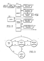
- the output from the input edge detector 10 is input to a pattern state memory 12 which is initially in an idle state as shown in Fig. 3.
- the pattern state memory 12 Upon receipt of an output indicative of a leading pulse edge of the input signal, the pattern state memory 12 starts duration testing by enabling a time duration counter 14.
- the time duration counter 14 counts clock pulses at a predetermined frequency which is high enough to assure detection of the pulse edges of the shortest anticipated pulse in the input signal.
- the pattern state memory 12 receives a trailing pulse edge signal from the input edge detector 10 after a predetermined minimum count is reached by the time duration counter 14, and before a maximum predetermined count is reached, the pattern state memory increments a valid pulse counter 16. If the pattern state memory 12 receives a trailing pulse edge signal from the input edge detector 10 before the predetermined minimum count is reached by the time duration counter 14, the count of the valid pulse counter 16 is checked to determine whether the proper number of consecutive pulses have been counted. If the proper number of pulses have been counted, the pattern state memory 12 may continue the time duration counter 14 to time a delay interval and a pattern found indication is held in the pattern state memory.
- the pattern found register 18 is enabled by an output from the time duration counter to generate a valid pulse output at a proper predetermined time with respect to the input signal, i.e., corresponding to a vertical sync time in a television signal to provide proper vertical timing.
- the valid pulse output from the pattern found register 18 is input to a latch 20 before being input to a signal state memory 22.
- the receipt of the valid pulse output by the signal state memory 22 starts a time interval counter 24 and increments a valid input counter 26. If the count of the time interval counter 24 exceeds a maximum value before the next valid pulse output from the pattern found register 18 is received, then both the valid input and time interval counters 26, 24 are reset. Otherwise for each valid pulse output received the valid input counter 26 is incremented and the time interval counter 24 is reset.
- a signal presence indicator OK is generated.
- the signal state memory 22 uses the valid input counter 26 to count missing valid pulse outputs, i.e., the valid input counter increments for each time that the time interval counter 24 exceeds the maximum value without receiving the valid pulse output from the pattern found register 18.
- the valid input counter 26 reaches a second predetermined count indicative of the number of consecutive cycles of the time interval counter 24 without receiving the valid pulse output from the pattern found register 18, then the signal state memory 22 generates a signal absence indicator /OK.
- a PAL vertical sync has a pattern of five wide negative pulses in sequence as opposed to six wide negative pulses for NTSC.
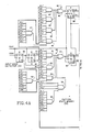
- the input signal CSIN is the television composite sync signal.
- D-type flip-flops 30, 32 make up the input edge detector 10.
- the flip-flops 30, 32 are connected in series with CSIN input in the D input of the first flip-flop and the Q output of the first flip-flop connected to the D input of the flip-flop.
- the negative, or leading, edge of pulses in CSIN is detected by combining the respective Q/ and Q outputs.
- the next clock pulse of CLK1 transfers the existing inputs to the output so that the Q output of the second flip-flop 32 is still high when the Q/ output of the first flip-flop goes high.
- the period of CLK1 is less than the pulse width of the shortest pulse of CSIN to assure that all pulse edges are detected.
- the pattern state memory 12 has two J-K flip-flops 38, 40 to provide the necessary four state outputs.
- the respective J-K inputs are connected to respective logic circuits 42, 50 consisting of AND gates 43-47, OR gate 48 and AND gates 51-56, OR gate 57, respectively.
- the logic circuits 42, 50 provide the combinational logic for switching states of the pattern state memory 12.
- the pattern state memory flip-flops 38, 40 are clocked by CLK1 to change state whenever a logical "1" is present at the J-K inputs.
- the pattern state memory flip-flops 38, 40 are reset by VBP when a valid pattern is found.
- AND gate 43 provides an input to flip-flop 38 via OR gate 48 when the state of the pattern state memory 12 is even and a leading negative edge is detected to switch the state to the next higher odd state.
- AND gate 44 provides an input to flip-flop 38 via OR gate 48 when CSIN is high, the state is "1", and the number of pulses in the pattern is less than 4 to switch the state to "0".
- AND gate 45 provides an input to flip-flop 38 via OR gate 48 when CSIN is high, the state is "1" and the number of pulses counted in the pattern is even to switch the state to "0".
- AND gates 46, 47 provide an input to flip-flop 38 via OR gate 48 and AND gates 55, 56 provide an input to flip-flop 40 via OR gate 57 when CSIN is low, i.e., in the middle of a pulse, the state is "1", and the minimum duration value from the time duration counter 14 is achieved to switch the state to "2".
- AND gate 51 provides an input to flip-flop 40 via OR gate 57 when there is a leading pulse edge of CSIN detected and the state is "2" to switch the state to "0".
- AND gate 51 provides an input to flip-flop 40 via OR gate 57 when CSIN is high, the state is "1" and the number of consecutive pulses counted is equal to five to switch the state to "3".
- AND gates 53, 54 provide an input to flip-flop 40 via OR gate 57 when the state is "2" and the maximum pulse width duration is exceeded to switch the state to "0".
- the valid pulse counter 16 has three J-K flip-flops 58, 60, 62 which act as a ripple counter which is incremented when the negative pulse edge of CSIN is detected commencing with the first negative transition after the initial valid pulse width is detected.
- Logic circuit 64 consisting of AND gates 65-67, OR gate 68 connected to the inputs of the first flip-flop 58, causes the counter 16 to increment when the count value is odd or when a total count of six has not been achieved while the state is "2".
- AND gates 69, 70 are connected to respective inputs of the subsequent flip-flops 60, 62 so that the pulse counter 16 increments up to six for each detected leading edge of CSIN while in state "2".
- the valid pulse counter 16 is reset via AND gate 72 whenever the state is "0".
- the time duration counter 14 consisting of flip-flops 74-81 and AND gates 82-87, counts the pulses of CLK1 so long as the state is not "0" as provided by NAND gate 88 to the input of the first flip-flop.
- the time duration counter 14 is reset via AND gate 90 on the leading edge of a pulse of CSIN when the state is even.
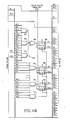
- the pattern found output pulse register 18 consists of a D-type flip-flop 92 clocked by CLK1 according to the input from AND gates 94, 96. These AND gates 94, 96 provide a logical "1" to the D input of the flip-flop 92 when the state is "3" and the duration from the duration counter 14 is equal to the desired time delay.
- the output from the pattern found register 18 is a valid pulse output VBP which indicates that the predetermined vertical sync pulse pattern has been identified.
- the VBP pulse is input via AND gate 100 and OR gate 102 to the inputs of a J-K flip-flop 104, which is the input latch 20, when the Q output of the flip-flop is low to switch the Q output high upon receipt of the next CLK1 pulse.
- the latch flip-flop 104 is "reset” when the time duration counter 24 reaches its maximum count while still in state "0".
- the signal state memory 22 has a single J-K flip-flop 110 for the necessary two states with inputs via AND gates 106, 107 and OR gate 108.
- the state flip-flop 110 When the state is "0", the output of the latch flip-flop 104 indicates a received VBP pulse and the count of the valid input counter 26 is four, the state flip-flop 110 is switched from state “0" to state “1” upon being clocked by a low speed clock CLK2. While in state “1” the state flip-flop 110 is switched to state “0” when the valid input counter 26 reaches its maximum count.
- J-K flip-flops 112-116 with associated input logic circuit 118 make up the valid input counter 26.
- AND gates 119, 123, 127 via respective OR gates 122, 126, 130 provide the inputs to the respective flip-flops 112-116 to count the number of consecutive VBP pulses received by the input latch 20 when the state is "0".
- AND gates 120, 125, 129 via the respective OR gates 122, 126, 130 "reset” the respective flip-flops 112-116 to maintain the count at zero as long as the input signal is present as indicated by the state "1" condition.
- AND gates 121, 124, 128 via the OR gates 122, 126, 130 cause the respective flip-flops 112-116 to increment for each missing VBP pulse, i.e., a VBP pulse is not received before the duration counter 24 reaches its maximum count.
- the flip-flops 112-116 are also reset via AND gate 132 when the state is "0" and the time interval counter 24 reaches its maximum count.
- the time interval counter 24 is made up of J-K flip-flops 134-138 and AND gate 140 to count consecutive pulses of the low speed clock CLK2.
- the maximum count of the time interval counter 24 represents a maximum time interval greater than the repetition period of the vertical sync pattern.
- the flip-flops 134-138 are reset each time a valid pulse output VBP is received, i.e., nominally when a valid input signal is present before the time interval counter 24 reaches its maximum count.
- the output of the signal state memory flip-flop 110 is the signal presence indicator OK.
- the state diagrams of Figs. 3 and 5 further illustrate the operation of the digital timing generator.
- the pattern state memory 12 is initially in an idle state "0". The transition from state “0" to state “1" along path A occurs when the leading edge of a pulse is detected by the input edge detector 10. Simultaneously the time duration counter 14 is reset, the valid pulse counter 16 already having been reset by the transition into state "0". In state “1" the time duration counter 14 starts to count clock pulses. If the input signal transitions before a minimum count is achieved and the valid pulse count is not the desired value, state “1" transitions along path D to state "0" which resets the valid pulse counter 16.
- state "1" transitions along path B to state "2"
- the pulse width of the input signal pulse has exceeded a minimum width.
- the time duration counter 14 continues to count until either another leading edge signal occurs or a maximum count is achieved. If a leading edge signal is first detected and the valid pulse counter 16 has not exceeded the desired value, then the valid pulse counter is incremented, the time duration counter 14 is reset and state “2" transitions along path C to state "1". If the maximum count is achieved first, indicating that the pulse width is too long, state "2" transitions along path F to state "0", resetting the valid pulse counter 16.
- state "1" transitions along path E to state "3", indicating that a valid input pulse pattern has been detected.
- the time duration counter 14 continues to count up to the desired delay value, at which point a valid pulse output VBP is generated from the pattern found register 18 and state "3" transitions along path G to state "0".
- the output pulse VBP from the pattern found register 18 is input to the latch 20 to synchronize the pulse with the low rate input clock used for the valid signal identification.
- the signal state memory 22 is in state "0" indicating no signal present.
- the VBP pulse is received from the latch 20 and increments the valid input counter 26 if the count is less than a predetermined minimum value, indicated by path P. If the time interval counter 24 is over the maximum time before the VBP pulse is received, then the time interval valid input counters 24, 26 are reset following path Q, indicating no valid signal present. If the valid input counter 26 is equal to the minimum value when the VBP pulse is received, then state "0" transitions along path R to state "1" to indicate a valid signal present and both counters are reset.
- the present invention provides a digital timing generator using a state machine for determining the presence of a predetermined pulse pattern, and for indicating that a valid input signal is present based upon the repetition of the predetermined pulse pattern.
Landscapes
- Physics & Mathematics (AREA)
- Nonlinear Science (AREA)
- Engineering & Computer Science (AREA)
- Multimedia (AREA)
- Signal Processing (AREA)
- Television Signal Processing For Recording (AREA)
- Manipulation Of Pulses (AREA)
- Synchronizing For Television (AREA)
Applications Claiming Priority (2)
| Application Number | Priority Date | Filing Date | Title |
|---|---|---|---|
| US19081 | 1987-02-25 | ||
| US07/019,081 US4763341A (en) | 1987-02-25 | 1987-02-25 | Digital timing using a state machine |
Publications (2)
| Publication Number | Publication Date |
|---|---|
| EP0280254A2 true EP0280254A2 (de) | 1988-08-31 |
| EP0280254A3 EP0280254A3 (de) | 1989-07-26 |
Family
ID=21791318
Family Applications (1)
| Application Number | Title | Priority Date | Filing Date |
|---|---|---|---|
| EP88102638A Withdrawn EP0280254A3 (de) | 1987-02-25 | 1988-02-23 | Digitale Zeitschaltung mit einem endlichen Automaten |
Country Status (3)
| Country | Link |
|---|---|
| US (1) | US4763341A (de) |
| EP (1) | EP0280254A3 (de) |
| JP (1) | JPS63314075A (de) |
Cited By (4)
| Publication number | Priority date | Publication date | Assignee | Title |
|---|---|---|---|---|
| GB2270177A (en) * | 1992-08-31 | 1994-03-02 | Silicon Systems Inc | Programmable system for the synchronization of an electronic angular position indicator |
| DE10024783A1 (de) * | 2000-05-19 | 2001-11-22 | Micronas Munich Gmbh | Digitaler Taktgenerator |
| EP1521364A1 (de) * | 2003-09-29 | 2005-04-06 | EM Microelectronic-Marin SA | Verfahren und Vorrichtung zur Filterung von durch einen Piezoelektrischen Beschleunigungsmesser erzeugten Signalen, und Anwendung auf einem tragbaren Gegenstand wie zum Beispiel eine Uhr |
| US10642673B2 (en) | 2018-01-02 | 2020-05-05 | International Business Machines Corporation | Hardware error detection on a high-speed serial connection |
Families Citing this family (13)
| Publication number | Priority date | Publication date | Assignee | Title |
|---|---|---|---|---|
| US4922352A (en) * | 1986-11-21 | 1990-05-01 | Hewlett-Packard Company | Block pattern detection circuitry |
| US4860098A (en) * | 1988-09-19 | 1989-08-22 | The Grass Valley Group, Inc. | Video discrimination between different video formats |
| US5058140A (en) * | 1990-03-12 | 1991-10-15 | International Business Machines Corporation | Self-correcting serial baud/bit alignment |
| KR950007267B1 (ko) * | 1990-10-16 | 1995-07-07 | 삼성전자주식회사 | 리모콘신호의 펄스폭 측정회로 |
| US5224129A (en) * | 1990-10-31 | 1993-06-29 | Tektronix, Inc. | Method of synchronizing signals of a pulse generator |
| JP3395210B2 (ja) * | 1992-06-30 | 2003-04-07 | ソニー株式会社 | 同期信号検出器及び同期信号検出方法 |
| US5317215A (en) * | 1992-12-01 | 1994-05-31 | 3Com Corporation | Method and apparatus for frequency discriminating computer network signals |
| JPH07135664A (ja) * | 1993-11-09 | 1995-05-23 | Funai Electric Co Ltd | 映像信号判定回路 |
| US5615237A (en) * | 1994-09-16 | 1997-03-25 | Transwitch Corp. | Telecommunications framer utilizing state machine |
| TW255079B (en) * | 1994-09-30 | 1995-08-21 | At & T Corp | Communications unit with data and clock recovery circuit |
| JP4045596B2 (ja) * | 2004-01-30 | 2008-02-13 | 船井電機株式会社 | リモコン受信装置及びそのリモコン信号判別方法 |
| US7719256B1 (en) * | 2008-03-20 | 2010-05-18 | The United States Of America As Represented By The Secretary Of The Navy | Method for determining a separation time |
| CN110570676B (zh) * | 2019-08-27 | 2021-01-01 | 苏州云控车路科技有限公司 | 一种基于单片机的交通信号灯状态监测系统 |
Family Cites Families (11)
| Publication number | Priority date | Publication date | Assignee | Title |
|---|---|---|---|---|
| US3686634A (en) * | 1971-04-02 | 1972-08-22 | Esb Inc | Pulse rate monitor and indicator system utilizing a burst pulse counter and a pulse internal counter |
| US4651332A (en) * | 1972-06-02 | 1987-03-17 | The United States Of America As Represented By The Secretary Of The Navy | Sector scan computer |
| NO132123C (de) * | 1973-04-13 | 1975-09-17 | Standard Tel Kabelfab As | |
| JPS5321517A (en) * | 1976-08-12 | 1978-02-28 | Nippon Television Ind Corp | Synchronizing signal selection circuit |
| CA1105609A (en) * | 1977-05-09 | 1981-07-21 | Nobukazu Hosoya | Line sampling circuit for television receiver |
| JPS53149076A (en) * | 1977-06-01 | 1978-12-26 | Sony Corp | Digital frequency detecting circuit |
| DE3037987C2 (de) * | 1980-10-08 | 1985-07-25 | Philips Patentverwaltung Gmbh, 2000 Hamburg | Schaltungsanordnung zum Ermitteln eines Impulses bestimmter Mindestlänge in einem Impulsgemisch |
| JPS60113585A (ja) * | 1983-11-24 | 1985-06-20 | Citizen Watch Co Ltd | 同期信号発生回路 |
| JPS61114658A (ja) * | 1984-11-09 | 1986-06-02 | Hitachi Ltd | 垂直同期信号分離回路 |
| DE3443925C1 (de) * | 1984-12-01 | 1986-01-30 | Philips Patentverwaltung Gmbh, 2000 Hamburg | Schaltungsanordnung zum Unterscheiden der beiden Halbbilder in einem Fernsehsignal |
| US4692710A (en) * | 1985-09-04 | 1987-09-08 | Electronic Design & Research, Inc. | Fundamental and harmonic pulse-width discriminator |
-
1987
- 1987-02-25 US US07/019,081 patent/US4763341A/en not_active Expired - Fee Related
-
1988
- 1988-02-23 EP EP88102638A patent/EP0280254A3/de not_active Withdrawn
- 1988-02-25 JP JP63043236A patent/JPS63314075A/ja active Pending
Cited By (8)
| Publication number | Priority date | Publication date | Assignee | Title |
|---|---|---|---|---|
| GB2270177A (en) * | 1992-08-31 | 1994-03-02 | Silicon Systems Inc | Programmable system for the synchronization of an electronic angular position indicator |
| GB2270177B (en) * | 1992-08-31 | 1995-11-22 | Silicon Systems Inc | Programmable system for the synchronization of an electronic angular position indicator |
| DE10024783A1 (de) * | 2000-05-19 | 2001-11-22 | Micronas Munich Gmbh | Digitaler Taktgenerator |
| DE10024783C2 (de) * | 2000-05-19 | 2002-05-08 | Micronas Munich Gmbh | Digitaler Taktgenerator |
| US7339412B2 (en) | 2000-05-19 | 2008-03-04 | Micronas Gmbh | Digital clock generator |
| EP1521364A1 (de) * | 2003-09-29 | 2005-04-06 | EM Microelectronic-Marin SA | Verfahren und Vorrichtung zur Filterung von durch einen Piezoelektrischen Beschleunigungsmesser erzeugten Signalen, und Anwendung auf einem tragbaren Gegenstand wie zum Beispiel eine Uhr |
| US7143012B2 (en) | 2003-09-29 | 2006-11-28 | Em Microelectronic-Marin Sa | Method and device for filtering signals produced by an accelerometer of the piezo-electric type, and application to a portable object such as a watch |
| US10642673B2 (en) | 2018-01-02 | 2020-05-05 | International Business Machines Corporation | Hardware error detection on a high-speed serial connection |
Also Published As
| Publication number | Publication date |
|---|---|
| JPS63314075A (ja) | 1988-12-22 |
| US4763341A (en) | 1988-08-09 |
| EP0280254A3 (de) | 1989-07-26 |
Similar Documents
| Publication | Publication Date | Title |
|---|---|---|
| US4763341A (en) | Digital timing using a state machine | |
| KR950005054B1 (ko) | 기수/우수의 필드 검출장치 | |
| CN1040604C (zh) | 视频信号的奇数/偶数场检测器 | |
| JPS61134183A (ja) | テレビジヨン信号のフイールド識別回路 | |
| KR100236887B1 (ko) | 비디오 신호 동기펄스 검출기 | |
| US4684988A (en) | Circuit arrangement for detecting the vertical blanking periods in a picture signal | |
| EP0927492A1 (de) | Verzögerungskorrekturschaltung | |
| JPH06204993A (ja) | クロック断検出回路 | |
| JPS60111577A (ja) | 垂直同期装置 | |
| GB2129249A (en) | Apparatus for generating a signal for driving the field deflection in a picture reproducing device | |
| JP2932967B2 (ja) | 映像信号の方式自動判別方法とその装置 | |
| JPH0865576A (ja) | カメラ映像切換装置 | |
| KR19980703637A (ko) | 수직 동기화 신호 검출기 | |
| JP2721691B2 (ja) | 水平期間識別装置 | |
| EP0242917A1 (de) | Korrekturschaltung für Synchronisierungssignale eines Fernsehsignals | |
| JPH03216076A (ja) | 同期分離回路 | |
| JPH0319576A (ja) | フレーム検出回路 | |
| JP2549002B2 (ja) | 映像信号取り込み回路 | |
| JP3745934B2 (ja) | カラーキラー検波器 | |
| JPH071921B2 (ja) | 奇・偶フイ−ルド判別装置 | |
| JPS594333Y2 (ja) | ライトペンの視野位置検出装置 | |
| JPS63290077A (ja) | フィ−ルド判別回路 | |
| JPH01316073A (ja) | フィールド検出回路およびフレーム検出回路 | |
| JPH07162898A (ja) | 映像信号品質監視回路および方法 | |
| JPH04196713A (ja) | パルス信号弁別回路 |
Legal Events
| Date | Code | Title | Description |
|---|---|---|---|
| PUAI | Public reference made under article 153(3) epc to a published international application that has entered the european phase |
Free format text: ORIGINAL CODE: 0009012 |
|
| AK | Designated contracting states |
Kind code of ref document: A2 Designated state(s): DE FR GB NL |
|
| PUAL | Search report despatched |
Free format text: ORIGINAL CODE: 0009013 |
|
| AK | Designated contracting states |
Kind code of ref document: A3 Designated state(s): DE FR GB NL |
|
| 17P | Request for examination filed |
Effective date: 19890711 |
|
| 17Q | First examination report despatched |
Effective date: 19900807 |
|
| STAA | Information on the status of an ep patent application or granted ep patent |
Free format text: STATUS: THE APPLICATION IS DEEMED TO BE WITHDRAWN |
|
| 18D | Application deemed to be withdrawn |
Effective date: 19901218 |