EP0281155A2 - AD-Wandler - Google Patents
AD-Wandler Download PDFInfo
- Publication number
- EP0281155A2 EP0281155A2 EP19880103396 EP88103396A EP0281155A2 EP 0281155 A2 EP0281155 A2 EP 0281155A2 EP 19880103396 EP19880103396 EP 19880103396 EP 88103396 A EP88103396 A EP 88103396A EP 0281155 A2 EP0281155 A2 EP 0281155A2
- Authority
- EP
- European Patent Office
- Prior art keywords
- signal
- vin
- terminal
- analog input
- input signal
- Prior art date
- Legal status (The legal status is an assumption and is not a legal conclusion. Google has not performed a legal analysis and makes no representation as to the accuracy of the status listed.)
- Granted
Links
Images




Classifications
-
- H—ELECTRICITY
- H03—ELECTRONIC CIRCUITRY
- H03M—CODING; DECODING; CODE CONVERSION IN GENERAL
- H03M1/00—Analogue/digital conversion; Digital/analogue conversion
- H03M1/12—Analogue/digital converters
-
- H—ELECTRICITY
- H03—ELECTRONIC CIRCUITRY
- H03M—CODING; DECODING; CODE CONVERSION IN GENERAL
- H03M1/00—Analogue/digital conversion; Digital/analogue conversion
- H03M1/12—Analogue/digital converters
- H03M1/1205—Multiplexed conversion systems
- H03M1/121—Interleaved, i.e. using multiple converters or converter parts for one channel
- H03M1/1215—Interleaved, i.e. using multiple converters or converter parts for one channel using time-division multiplexing
-
- H—ELECTRICITY
- H03—ELECTRONIC CIRCUITRY
- H03M—CODING; DECODING; CODE CONVERSION IN GENERAL
- H03M1/00—Analogue/digital conversion; Digital/analogue conversion
- H03M1/12—Analogue/digital converters
- H03M1/14—Conversion in steps with each step involving the same or a different conversion means and delivering more than one bit
- H03M1/145—Conversion in steps with each step involving the same or a different conversion means and delivering more than one bit the steps being performed sequentially in series-connected stages
- H03M1/146—Conversion in steps with each step involving the same or a different conversion means and delivering more than one bit the steps being performed sequentially in series-connected stages all stages being simultaneous converters
Definitions
- the present invention relates to an analog-to-digital converter and, more particularly, to an analog-to-digital converter used in equipment, such as a video signal processor, which requires a high-speed conversion operation.
- a so-called flush or parallel A/D converter described in literature 1 (Monolithic Expandable 6 bit 20 MHz CMOS/SOS A/D Converter", ANDREW G.F. DINGWALL, MEMBER, IEEE, IEEE JOURNAL OF SOLID-STATE CIRCUITS, VOL. SC-14, NO. 6, DECEMBER 1979), and a so-called sub-ranging or serial-parallel A/D converter described in literature 2 (“An 8-MHz CMOS Subranging 8-bit A/D Converter”, ANDREW G.F. DINGWALL, MEMBER, IEEE, AND VICTOR ZAZZU, MEMBER, IEEE, IEEE JOURNAL OF SOLID-STATE CIRCUITS, VOL. SC-20, NO. 6, DECEMBER 1985) are known typical high-speed A/D (analog-to-digital) converters.
- Fig. 4 shows the principle of a parallel A/D converter.
- An A/D converter converts an analog input signal into an n-bit binary code, and comprises 2 n -1 parallel voltage comparators 10(1) to 10(2 n -1).
- One input of each comparator commonly receives an analog input signal, and the other input thereof receives reference voltage signals, having different voltage values, generated by reference voltage generator 11.
- Each voltage comparator 10 compares the voltage value of the analog input signal with the given reference voltage, and supplies the comparison result to encoder 12.
- Encoder 12 outputs a digital signal corresponding to the comparison results, i.e., an n-bit binary code.
- the parallel A/D converter described above can perform very high-speed A/D conversion.
- a large number of voltage comparators 10, corresponding to the number of quantization steps performed, i.e., 2 n -1, is required for converting an analog signal into an n-bit digital signal. Consequently, this arrangement is quite complex, and an IC chip area required to form the converter is increased in the case of IC formation.
- Fig. 5 shows a serial-parallel A/D converter.
- This converter divides an n-bit binary code into upper a bits and lower b bits, so that A/D conversion relating to the upper a bits is performed by upper-bit A/D conversion section (ADC) 13, after which that relating to the lower b bits is performed by lower-bit A/D conversion section (ADC) 14, on the basis of the conversion result of the upper a bits.
- ADC upper-bit A/D conversion section
- ADC lower-bit A/D conversion section
- upper-bit A/D conversion section 13 comprises reference voltage generator 11a, voltage comparators 10a, and encoder 12a, in the same manner as the parallel A/D converter shown in Fig. 4.
- the number of voltage comparators 10a provided is 2 a -1.
- the number of voltage comparators (10b) provided in A/D conversion section 14 is 2 b -1.
- the total number of voltage comparators is 2 a -1 + 2 b -1, and the arrangement can be simpler than that of the parallel A/D converter shown in Fig. 4, which requires 2 n -1 voltage comparators (2 n -1 > (2 a -1 + 2 b -1)).
- each reference voltage generated by voltage generator 11b, provided in A/D conversion section 14
- the conversion operation of A/D conversion section 14 is performed after the conversion in A/D conversion section 13 has been completed.
- A/D conversion sections 13 and 14 cannot execute their conversion operations simultaneously, with the result that the time required to achieve the conversion is doubled as compared to that of the parallel A/D converter shown in Fig. 4.
- the present invention has been conceived in consideration of the above situation and has as its object to provide an A/D converter which can eliminate the conflicting drawbacks of the conventional A/D converters, i.e., the increase in the number of voltage comparators and a complicated circuit arrangement for the purpose of high-speed conversion, and a decrease in conversion rate (conversion speed) when the number of voltage comparators is decreased, and which can perform high-speed A/D conversion by means of a single circuit arrangement.
- the A/D converter of the present invention comprises: a first A/D conversion circuit for converting an analog input signal and determining the upper bits of an n-bit binary code; first and second sample-hold circuits which are alternatively switched each time the first A/D conversion circuit samples the analog input signal, and which sample and hold the analog input signal, in synchronism with the sampling timing of the first A/D conversion circuit; and a second A/D conversion circuit.
- the second A/D conversion circuit includes a reference voltage generator for generating a reference voltage of a predetermined value, based on the content of the binary code obtained by the first A/D conversion circuit, a voltage comparator for comparing the reference voltage value with the voltage value of the analog input signal held in either the first or second sample-hold circuit, which sample and hold the analog input signal corresponding to the binary code, and an encoder for encoding the comparison result, output from the voltage comparator, into a binary code and determining the lower bits of the n bits.
- the other sample-hold circuit supplies, to the second A/D conversion circuit, a value which was sampled and held one sampling period before. Therefore, while the first A/D conversion circuit is executing an A/D conversion, the second A/D conversion circuit can perform A/D conversion one sampling period before the A/D conversion currently executed by the first A/D conversion circuit. In this manner, the first and second A/D conversion circuits are operated in a pipeline manner (i.e., operated parallel along the time base), thus making possible high-speed A/D conversion.
- Fig. 1 shows an A/D converter according to an embodiment of the present invention.
- A/D conversion relating to upper a bits is performed by upper-bit A/D conversion section (ADC) 13, and that relating to lower b bits is performed by lower-bit A/D conversion section (ADC) 14.
- ADC upper-bit A/D conversion section
- ADC lower-bit A/D conversion section
- This feature is the same as that of the conventional A/D converter as shown in Fig. 5.
- pipelining of ADCs 13 and 14 is performed using two sample-hold (S/H) circuits 15a and 15b which are connected to the input terminal of ADC 14.
- S/H sample-hold
- S/H circuits 15a and 15b are switched by two switches, S1 and S2, between a sample-hold operation for analog input signal Vin and an output operation for the sampled and held value. More specifically, when one S/H circuit, for example, 15a, samples and holds analog input signal Vin, the other S/H circuit, 15b, supplies ADC 14 with a value (V15b) which was sampled and held one sampling period before.
- switches S1 and S2 are switched every sample operation, when ADC 13 corresponding to the upper a bits samples analog input signal Vin, one of S/H circuits 15a and 15b samples the same analog input signal Vin.
- switches S1 and S2 are switched, and ADC 14 receives result D13 of the upper a bits and sample value V15a or V15b of analog input signal Vin. This value has been sampled and held by S/H circuit 15a or 15b, and corresponds to the upper a bits.
- ADC 14 compares reference voltages, each determined by the content of the upper a bits, with the voltage value (V15a or V15b) of the analog input signal, using 2 b -1 voltage comparators (10b), and converts the comparison results into a binary code, by way of an encoder (12b), to determine the lower b bits.
- the upper a bits from ADC 13 are delayed by delay circuit 16 by the time required to complete the A/D conversion in ADC 14 so as to be synchronized with the lower b bits from ADC 14, and are output as an n-bit binary code.
- ADC 14 executes the A/D conversion
- ADC 13 executes the A/D conversion of the next analog input signal, one of S/H circuits 15a and 15b holding the sample value of this analog input signal.
- upper- and lower-bit ADCs 13 and 14 are operated in a pipeline manner, with the result that the A/D conversion rate can be as high as that of the parallel A/D converter shown in Fig. 4.
- the total number of voltage comparators provided in this A/D converter is 2 a -1 + 2 b -1, and can be greatly decreased as compared to the parallel A/D converter which requires 2 n -1 comparators.
- Fig. 2 shows an A/D converter according to another embodiment of the present invention.
- the A/D converter of this embodiment has basically the same arrangement as that of the A/D converter shown in Fig. 1, except that in place of independent S/H circuits 15a and 15b, two chopper voltage comparator sections 21A and 21B are arranged as 2 b -1 voltage comparators 21 provided in lower-bit ADC 140 for lower b bits, and have a sample-hold function.
- Chopper voltage comparator section 21A comprises inverter I1, capacitor C1, and switches S11 to S13.
- Chopper voltage comparator section 21B comprises inverter I2, capacitor C2, and switches S21 to S23. The outputs from these voltage comparator sections are selected in alternate fashion, and the selected output is supplied to encoder 22.
- Switches S10 to S13 and S21 to S23 are controlled by the clock signals shown in Figs. 3A to 3G.
- reference symbol ⁇ 11 denotes a clock signal for controlling switches S11; ⁇ 12, a clock signal for controlling switches S12 and S13; ⁇ 21, a clock signal for controlling switch S21; ⁇ 22, a clock signal for controlling switches S22 and S23; and ⁇ 10, a clock signal for controlling switch S10.
- Reference symbols ⁇ 01 and ⁇ 02 (Figs. 3A and 3B) denote control clock signals for upper-bit ADC 13, one period of clock signal ⁇ 01 or ⁇ 02 corresponding to the delay time of delay circuit 16.
- voltage comparator section 21B the sample-hold operation of an analog input signal is performed in response to clock signals ⁇ 21 and ⁇ 22 (Figs. 3E and 3F), and comparison between the analog input signal (corresponding to V15b in Fig. 1) held in capacitor C2 and reference voltage signal Vref(1) is executed.
- clock signal ⁇ 10 goes to "0" level, and comparison result V21(1) is sent to encoder 12B via switch S10.
- reference voltage generator 16 and encoder 12b can employ those disclosed in Fig. 2 (p.927) or Fig. 4 (p.929) of literature 1 and Fig. 2 (p.1140) of literature 2 presented in "Background of the Invention".
- the upper- and lower-bit ADCs can be operated in the pipelining manner.
- the same operating speed (sampling period) as in the parallel A/D converter can be obtained although the number of comparators is greatly reduced.
- Fig. 6 is a block diagram showing in detail the arrangement of an A/D converter according to another embodiment of the present invention.
- Figs. 7A to 7F are timing charts for explaining the operation of the A/D converter shown in Fig. 6.
- reference voltage generator 11a in upper-bit ADC 13 outputs 2 a -1 reference voltages Vr(1) to Vr(2 a -1).
- Reference voltage Vr(1) is supplied to one terminal of capacitor CO through switch SO1 which is turned on/off in response to clock signal ⁇ 01 (Fig. 7A).
- the other terminal of capacitor CO is connected to the input terminal of inverter IO.
- the output terminal of inverter IO is connected to its input terminal through switch SO3 which is turned on/off in response to clock signal ⁇ 02 (Fig. 7B).
- Analog signal Vin to be A/D converted is supplied to one terminal of capacitor CO through switch SO2 which is turned on/off in response to clock signal ⁇ 02.
- Circuit components SO1 to SO3, CO, and IO of voltage comparator 20(1) correspond to circuit components S11 to S13, C1, and I1 of voltage comparator section 21A shown in Fig. 2, and the circuit operation thereof is the same except for clock timings.
- Voltage comparator 20(1) supplies "1"-level signal V20(1) to encoder 12a when analog signal Vin exceeds reference voltage Vr(1).
- voltage comparator 20(2) supplies "1"-level signal V20(2) to encoder 12a when analog signal Vin exceeds reference voltage Vr(2).
- Voltage comparator 20(2 a -1) supplies "1"-level signal V20(2 a -1) to encoder 12a when analog signal Vin exceeds reference voltage Vr(2 a -1).
- Encoder 12a supplies, to reference voltage generator 11b in lower-bit ADC 140, a-bit digital signal D13 corresponding to the combination of "1" levels of input signals V20(1) to V20(2 a -1).
- Reference voltage generator 11b outputs 2 b -1 reference voltages Vr(1) to Vr(2 b -1) which change in proportion to the content (value) of signal D13.
- ADC 140 shown in Fig. 6 are substantially the same as those of ADC 140 shown in Fig. 2.
- switch S10 in Fig. 2 which is switched in response to clock signal ⁇ 10 corresponds to switches S14 and S24 which are switched in response to clock signals ⁇ 11 and ⁇ 21 (Figs. 7C and 7E).
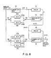
- Fig. 8 shows a schematic arrangement of an A/D converter according to still another embodiment of the present invention.
- the A/D conversion section is divided into two, but in the embodiment shown in Fig. 8, the A/D conversion section is divided into three.
- FIG. 8 upper a bits of the digital conversion value of analog input Vin are obtained by ADC 13, and medium b bits thereof are obtained by ADC 14.
- Upper a-bit data D13 is delayed by delay circuit 16 by a time corresponding to one sampling clock (corresponding to one period of clock signal ⁇ 01 shown in Fig. 10) for the purpose of synchronization, and is synthesized with medium b-bit data D14.
- Synthesized upper-medium a+b-bit data D140 is delayed by delay circuit 18 by a time corresponding to one sampling clock (corresponding to one period of clock signal ⁇ 01 in Fig. 10) for the purpose of synchronization, and is then synthesized with lower c-bit data D19.
- Synthesized upper-medium-lower a+b+c-bit data serves as n-bit digital output Dout.
- lower-bit ADC 19 in Fig. 8 can be basically the same as that of lower-bit ADC 14 shown in Fig. 1. However, the operation timing of ADC 19 and that of sample-hold (S/H) circuits 17a to 17c used therewith are slightly different from those of ADC 14 in Fig. 1 and S/H circuits 15a and 15c used therewith.
- S/H sample-hold
- circuit components 15a, 15b, 14b, S1, and S2 in Fig. 8 functionally correspond to medium-bit ADC 140 in Fig. 9, and circuit components 17a, 17b, 17c, 19b, S3, and S4 in Fig. 8 functionally correspond to lower-bit ADC 190 in Fig. 9.
- Lower-bit ADC 190 for generating lower c-bit data is arranged as follows.
- reference voltage generator 11c in ADC 190 receives signal D140 as synthesized data of delayed data of a-bit digital signal D13 from encoder 12a and b-bit digital signal D14 from encoder 12b.
- Generator 11c outputs 2 c -1 reference voltages Vs(1) to Vs(2 c -1) which change proportional to the content (value) of signal D140.
- Reference voltage Vs(1) is supplied to one terminal of capacitor C10 through switch S31 which is turned on/off in response to clock signal ⁇ 31 (Fig. 10G).
- the other terminal of capacitor C10 is connected to the input terminal of inverter I10.
- Capacitor C10 holds a voltage corresponding to output V17a of S/H circuit 17a in Fig. 8.
- the output terminal of inverter I10 is connected to its input terminal through switch S33 which is turned on/off in response to clock signal ⁇ 32 (Fig. 10H).
- Analog signal Vin to be A/D converted is supplied to one terminal of capacitor C10 through switch S32 which is turned on/off in response to clock signal ⁇ 32.
- Circuit components S31 to S33, C10, and I10 in voltage comparator 22(1) correspond to circuit components S11 to S13, C1, and I1 in voltage comparator section 21A shown in Fig. 2, and performs the same circuit operation except for clock timings.
- Circuit components S31 to S33, C10, and I10 of voltage comparator 22(1) supply "1"-level signal V22(1) to encoder 12c when analog signal Vin exceeds reference voltage Vs(1) and clock signal ⁇ 31 is input.
- switch S10 in Fig. 2 which is switched by clock signal ⁇ 10 corresponds to switches S34, S44, and S54 which are switched in response to clock signals ⁇ 31, ⁇ 41, and ⁇ 51 (Figs. 10G, 10I, and 10K).
- Reference voltage Vs(1) is also supplied to one terminal of capacitor C20 through switch S41 which is turned on/off in response to clock signal ⁇ 41 (Fig. 10I).
- the other terminal of capacitor C20 is connected to the input terminal of inverter I20.
- Capacitor C20 holds a voltage corresponding to output V17b of S/H circuit 17b in Fig. 8.
- the output terminal of inverter I20 is connected to its input terminal through switch S43 which is turned on/off in response to clock signal ⁇ 42 (Fig. 10J).
- Analog signal Vin is supplied to one terminal of capacitor C20 through switch S42 which is turned on/off in response to clock signal ⁇ 42.
- Circuit components S41 to S43, C20, and I20 in voltage comparator 22(1) have the same arrangement as that of circuit components S31 to S33, C10, and I10, and perform the same circuit operation except for clock timings. Circuit components S41 to s43, C20, and I20 in voltage comparator 22(1) supply "1"-level signal V22(1) to encoder 12c when analog signal Vin exceeds Vs(1) and clock signal ⁇ 41 is input.
- Reference voltage Vs(1) is also supplied to one terminal of capacitor C30 through switch S51 which is turned on/off in response to clock signal ⁇ 51 (Fig. 10K).
- the other terminal of capacitor C30 is connected to the input terminal of inverter I30.
- Capacitor C30 holds a voltage corresponding to output V17c of S/H circuit 17c in Fig. 8.
- the output terminal of inverter I30 is connected to its input terminal through switch S53 which is turned on/off in response to clock signal ⁇ 52 (Fig. 10L).
- Analog signal Vin is supplied to one terminal of capacitor C30 through switch S52 which is turned on/off in response to clock signal ⁇ 52.
- Circuit components S51 to S53, C30, and I30 of voltage comparator 22(1) also have the same arrangement as that of circuit components S31 to S33, C10, and I10, and perform the same circuit operation except for clock timings. Circuit components S51 to S53, C30, and I30 of voltage comparator 22(1) supply "1"-level signal V22(1) to encoder 12c when analog signal Vin exceeds reference voltage Vs(1) and clock signal ⁇ 51 is input.
- voltage comparator 22(2 c -1) supplies "1"-level signal V22(2 c -1) to encoder 12c when analog signal Vin exceeds reference voltage Vs(2 c -1) and clock signals corresponding to clocks ⁇ 31 to ⁇ 51 are received.
- Encoder 12c outputs c-bit digital signal D19 corresponding to a combination of "1" levels of input signals V(1) to V22(2 c -1).
- the number of comparators (20 to 22) is larger than that of Fig. 2 or 6, but is greatly reduced as compared to the arrangement shown in Fig. 4. Further, the A/D conversion rate of the arrangement of Fig. 9 can be as high as that obtained by the arrangement of Fig. 2 or 6.
- the value of Vref(1) applied to switch S11 may differ from that applied to switch S21.
- the values respectively applied to switches S31, S41, and S51 may be different from one another.
- SW1 denotes a first switch which receives first analog input signal Vin1; and SW2, a second switch which receives second analog input signal Vin2.
- the output terminals of switches SW1 and SW2 are connected to each other, and the node therebetween is connected to one terminal (node N1) of first capacitor CO1.
- the other terminal (node N2) of first capacitor CO1 is connected to buffer amplifier BO having a high input impedance/low output impedance.
- the output terminal of buffer amplifier BO is connected to one terminal (node N3) of second capacitor CO2.
- the other terminal (node N4) of second capacitor CO2 is connected to the input terminal of inverting amplifier IO.
- Third switch SW3 is connected between the input and output terminals of inverting amplifier IO. Further additionally, the other terminal (N2) of first capacitor CO1 is connected to reference voltage generator 110 through fourth switch SW4.
- V4 is a voltage at the input terminal of inverting amplifier IO having gain "-K”
- can be considered to be reduced.
- a steady solution (a solution after a sufficient time has passed from when second, third, and fourth switches SW2 to SW4 are turned on) is calculated.
- Voltage V2 at the output terminal (node N2) of first capacitor CO1 is represented by:
- Voltage V3 at the input terminal (node N3) of second capacitor CO2 is represented by: where K2 is a voltage gain of buffer amplifier BO.
- Inverting amplifier IO can have various arrangements, as shown in Figs. 13 to 17.
- Buffer amplifier BO can have various arrangements, as shown in Figs. 18 to 23.
- An inverting amplifier shown in Fig. 13 is a CMOS inverter in which p- and n-channel transistors P and N are connected in series with each other, and their gates are commonly connected.
- An inverting amplifier shown in Fig. 14 is an n-channel MOS inverter in which constant current source 11X and n-channel transistor N are connected in series with each other.
- An inverting amplifier shown in Fig. 15 is a p-channel MOS inverter in which p-channel MOS transistor P and current source 12X are connected in series with each other.
- An inverting amplifier shown in Fig. 16 is a p-channel MOS inverter in which p-channel transistor P and resistor R are connected in series with each other.
- An inverting amplifier shown in Fig. 17 is an n-channel MOS inverter in which resistor R and n-channel MOS transistor N are connected in series with each other.
- a buffer amplifier shown in Fig. 20 is constituted by cascade-connecting n-channel inverter IVN in which current source 11X is connected in series with n-channel transistor N, and p-channel inverter IVP in which p-channel transistor P is connected in series with current source 12X.
- a buffer amplifier shown in Fig. 20 is constituted by cascade-connecting n-channel inverter IVN in which current source 11X is connected in series with n-channel transistor N, and p-channel inverter IVP in which p-channel transistor P is connected in series with current source 12X.
- connection relationship between n- and p-channel inverters IVN and IVP is reversed to that of Fig. 20.
- a buffer amplifier shown in Fig. 12 is constituted by cascade connecting the buffer amplifiers shown in Figs. 18 and 19.
- a buffer amplifier shown in Fig. 23 has the connection relationship of the circuits reversed to that of Fig. 22.
- Constant current sources 11X and 12X are realized by applying bias voltage VB or VB* to the gate of a p- or n-channel transistor, as shown in Figs. 24 and 25.
- Reference voltage generator 110 in Fig. 11 need only supply a constant voltage for at least a predetermined period of time while switch SW4 is kept on, and may employ either arrangement as follows.
- p-channel transistor P the gate and drain of which are connected to each other, is connected in series with n-channel transistor N, the drain and gate of which are connected to each other.
- voltage-dividing resistors R1 and R2 are series-connected between the VDD and VSS power supply nodes.
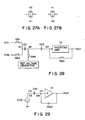
- third, and fourth switches SW2, SW3, and SW4 in Fig. 11 need only be CMOS switches (transfer gates) to which complementary clock signals 1 and 2 are supplied as gate signals, as shown in Fig. 27A.
- Switch SW1 can be a CMOS switch (Fig. 27B) to which clock signals ⁇ 2 and ⁇ 1 complementarily to switches SW2 to SW4 are supplied as gate signals.
- the input bias of buffer amplifier BO in the modification shown in Fig. 11 is supplied from reference voltage generator 110.
- reference voltage generator 110 can be a ground potential terminal.
- the circuit arrangement can be simplified, charges are migrated between capacitors CO1 and CO2 due to a stray capacitance of the input terminal of inverting amplifier IO. Therefore, the voltage comparator shown in Fig. 11 has better sensitivity than that of Fig. 28.
- the voltage comparators shown in Figs. 11 and 28 even if a signal input is a high-frequency signal, it can be held in a capacitor with high precision, and voltage comparison between the held signal (Vin2) and a reference signal (Vin1) can be satisfactorily performed. Addition of buffer amplifier BO allows an improvement of the sensitivity of the voltage comparator.
- the voltage comparators shown in Figs. 11 and 28 are suitable for an an A/D converter for a high-frequency signal such as a television signal.
Landscapes
- Engineering & Computer Science (AREA)
- Theoretical Computer Science (AREA)
- Analogue/Digital Conversion (AREA)
Applications Claiming Priority (2)
| Application Number | Priority Date | Filing Date | Title |
|---|---|---|---|
| JP62047733A JPH0810830B2 (ja) | 1987-03-04 | 1987-03-04 | アナログ―ディジタル変換器 |
| JP47733/87 | 1987-03-04 |
Publications (3)
| Publication Number | Publication Date |
|---|---|
| EP0281155A2 true EP0281155A2 (de) | 1988-09-07 |
| EP0281155A3 EP0281155A3 (de) | 1992-04-29 |
| EP0281155B1 EP0281155B1 (de) | 1995-10-18 |
Family
ID=12783540
Family Applications (1)
| Application Number | Title | Priority Date | Filing Date |
|---|---|---|---|
| EP88103396A Expired - Lifetime EP0281155B1 (de) | 1987-03-04 | 1988-03-04 | AD-Wandler |
Country Status (5)
| Country | Link |
|---|---|
| US (1) | US4893124A (de) |
| EP (1) | EP0281155B1 (de) |
| JP (1) | JPH0810830B2 (de) |
| KR (1) | KR900008820B1 (de) |
| DE (1) | DE3854582T2 (de) |
Cited By (6)
| Publication number | Priority date | Publication date | Assignee | Title |
|---|---|---|---|---|
| WO1996025798A3 (en) * | 1995-02-15 | 1996-11-21 | Analog Devices Inc | Analog-to-digital conversion with multiple charge redistribution conversions |
| US5668551A (en) * | 1995-01-18 | 1997-09-16 | Analog Devices, Inc. | Power-up calibration of charge redistribution analog-to-digital converter |
| EP0849883A1 (de) * | 1992-10-01 | 1998-06-24 | Matsushita Electric Industrial Co., Ltd. | Analog-Digital-Wandler |
| US5852415A (en) * | 1994-04-29 | 1998-12-22 | Analog Devices, Inc. | Charge redistribution analog-to-digital converter with system calibration |
| EP1239593A3 (de) * | 2001-03-09 | 2004-01-21 | Fujitsu Limited | A/D-Wandler |
| WO2011036529A3 (en) * | 2009-09-28 | 2011-05-19 | Arctic Silicon Devices, As | Input configuration for analog to digital converter |
Families Citing this family (29)
| Publication number | Priority date | Publication date | Assignee | Title |
|---|---|---|---|---|
| US5172117A (en) * | 1989-06-19 | 1992-12-15 | Linear Instruments | Analog to digital conversion using an integrater and a sample and hold circuit |
| US5059896A (en) * | 1989-09-25 | 1991-10-22 | General Electric Company | Electronic watthour meter |
| US5043732A (en) * | 1989-09-26 | 1991-08-27 | Analog Devices, Inc. | Analog-to-digital converter employing a pipeline multi-stage architecture |
| US5248973A (en) * | 1991-10-24 | 1993-09-28 | The Mitre Corporation | High-speed, high-resolution analog to digital converter subranging architecture |
| JPH05218868A (ja) * | 1992-02-03 | 1993-08-27 | Hitachi Ltd | 多段型ad変換器 |
| JP2995599B2 (ja) * | 1992-09-09 | 1999-12-27 | セイコーインスツルメンツ株式会社 | アナログデジタル変換方法 |
| JPH06260941A (ja) * | 1993-03-05 | 1994-09-16 | Mitsubishi Electric Corp | アナログ/デジタル変換装置 |
| JPH06268521A (ja) * | 1993-03-10 | 1994-09-22 | Fujitsu Ltd | A/dコンバータ |
| US5574457A (en) * | 1995-06-12 | 1996-11-12 | Motorola, Inc. | Switched capacitor gain stage |
| US5689260A (en) * | 1995-09-22 | 1997-11-18 | Lucent Technologies Inc. | Analog-to-digital converter using scaled signal to initialize coarse conversion circuit |
| JPH09186594A (ja) * | 1995-12-28 | 1997-07-15 | Fujitsu Ltd | コンパレータ、アナログ−デジタルコンバータ、半導体装置及び電圧比較方法 |
| US5726653A (en) * | 1996-01-22 | 1998-03-10 | Industrial Technology Research Institute | Tri-step analog-to-digital converter |
| JP2000036746A (ja) * | 1998-07-17 | 2000-02-02 | Nec Corp | A/d変換器 |
| GB9821091D0 (en) * | 1998-09-30 | 1998-11-18 | Koninkl Philips Electronics Nv | Analogue to digital converter |
| TW492100B (en) * | 2000-03-13 | 2002-06-21 | Disco Corp | Semiconductor wafer processing apparatus |
| JP2002118466A (ja) * | 2000-10-05 | 2002-04-19 | Mitsubishi Electric Corp | Ad変換回路 |
| US6549150B1 (en) | 2001-09-17 | 2003-04-15 | International Business Machines Corporation | Integrated test structure and method for verification of microelectronic devices |
| JP2003188726A (ja) * | 2001-12-17 | 2003-07-04 | Fujitsu Ltd | A/dコンバータ及びシステム及びコンパレータ |
| JP2004194066A (ja) * | 2002-12-12 | 2004-07-08 | Fujitsu Ltd | 増幅回路、比較回路、及びad変換回路 |
| US7088275B2 (en) * | 2003-12-31 | 2006-08-08 | Conexant Systems, Inc. | Variable clock rate analog-to-digital converter |
| JP2008042380A (ja) * | 2006-08-03 | 2008-02-21 | Matsushita Electric Ind Co Ltd | アナログ・ディジタル変換器 |
| TWI393042B (zh) * | 2009-08-11 | 2013-04-11 | Au Optronics Corp | 具高觸碰靈敏度之觸碰面板裝置與其觸碰定位方法 |
| JP5732031B2 (ja) * | 2012-12-26 | 2015-06-10 | 旭化成エレクトロニクス株式会社 | パイプライン型a/dコンバータ |
| US9219490B1 (en) | 2014-09-08 | 2015-12-22 | Lockheed Martin Corporation | Front end sample and hold circuit for a reconfigurable analog-to-digital converter |
| US9595974B1 (en) | 2014-09-08 | 2017-03-14 | Lockheed Martin Corporation | Reconfigurable wideband sub-ranging analog-to-digital converter |
| US9143146B1 (en) * | 2014-09-08 | 2015-09-22 | Lockheed Martin Corporation | Reconfigurable wideband sub-ranging analog-to-digital converter |
| US9088292B1 (en) | 2014-09-08 | 2015-07-21 | Lockheed Martin Corporation | Clocking scheme for reconfigurable wideband analog-to-digital converter |
| CN112748675A (zh) * | 2019-10-16 | 2021-05-04 | 重庆禾瑞佳森物联网科技有限责任公司 | 兼容多类型从机的单片机系统 |
| CN116015303A (zh) * | 2021-10-22 | 2023-04-25 | 深圳市中兴微电子技术有限公司 | 模数转换方法、模数转换器、基站 |
Family Cites Families (9)
| Publication number | Priority date | Publication date | Assignee | Title |
|---|---|---|---|---|
| FR2264432B1 (de) * | 1974-03-15 | 1976-12-17 | Thomson Csf | |
| JPS5242057A (en) * | 1975-09-30 | 1977-04-01 | Toshiba Corp | A-d convertor |
| US4232302A (en) * | 1978-08-24 | 1980-11-04 | Ohio Nuclear, Inc. | Video speed logarithmic analog-to digital converter |
| US4326192A (en) * | 1979-06-11 | 1982-04-20 | International Business Machines Corporation | Sequential successive approximation analog-to-digital converter |
| FR2481543A1 (fr) * | 1980-04-23 | 1981-10-30 | Thomson Csf | Codeur analogique numerique comportant un generateur de tension codee a transfert de charges |
| DE3021880A1 (de) * | 1980-06-11 | 1981-12-17 | Philips Patentverwaltung | Schaltungsanordnung fuer eine analog-digital-umwandler |
| JPS6029030A (ja) * | 1983-06-24 | 1985-02-14 | Hitachi Ltd | アナログ・デジタル変換器 |
| JPH0681048B2 (ja) * | 1984-03-21 | 1994-10-12 | 株式会社日立製作所 | A/d変換器 |
| US4745393A (en) * | 1985-09-25 | 1988-05-17 | Hitachi, Ltd | Analog-to-digital converter |
-
1987
- 1987-03-04 JP JP62047733A patent/JPH0810830B2/ja not_active Expired - Lifetime
-
1988
- 1988-03-02 US US07/163,025 patent/US4893124A/en not_active Expired - Lifetime
- 1988-03-04 KR KR1019880002228A patent/KR900008820B1/ko not_active Expired
- 1988-03-04 DE DE3854582T patent/DE3854582T2/de not_active Expired - Fee Related
- 1988-03-04 EP EP88103396A patent/EP0281155B1/de not_active Expired - Lifetime
Cited By (8)
| Publication number | Priority date | Publication date | Assignee | Title |
|---|---|---|---|---|
| EP0849883A1 (de) * | 1992-10-01 | 1998-06-24 | Matsushita Electric Industrial Co., Ltd. | Analog-Digital-Wandler |
| US5852415A (en) * | 1994-04-29 | 1998-12-22 | Analog Devices, Inc. | Charge redistribution analog-to-digital converter with system calibration |
| US5668551A (en) * | 1995-01-18 | 1997-09-16 | Analog Devices, Inc. | Power-up calibration of charge redistribution analog-to-digital converter |
| WO1996025798A3 (en) * | 1995-02-15 | 1996-11-21 | Analog Devices Inc | Analog-to-digital conversion with multiple charge redistribution conversions |
| US5621409A (en) * | 1995-02-15 | 1997-04-15 | Analog Devices, Inc. | Analog-to-digital conversion with multiple charge balance conversions |
| EP1239593A3 (de) * | 2001-03-09 | 2004-01-21 | Fujitsu Limited | A/D-Wandler |
| WO2011036529A3 (en) * | 2009-09-28 | 2011-05-19 | Arctic Silicon Devices, As | Input configuration for analog to digital converter |
| US8786475B2 (en) | 2009-09-28 | 2014-07-22 | Hittite Microwave Corporation | Input configuration for analog to digital converter |
Also Published As
| Publication number | Publication date |
|---|---|
| EP0281155A3 (de) | 1992-04-29 |
| JPS63215223A (ja) | 1988-09-07 |
| KR880012019A (ko) | 1988-10-31 |
| KR900008820B1 (ko) | 1990-11-30 |
| EP0281155B1 (de) | 1995-10-18 |
| DE3854582D1 (de) | 1995-11-23 |
| JPH0810830B2 (ja) | 1996-01-31 |
| US4893124A (en) | 1990-01-09 |
| DE3854582T2 (de) | 1997-01-09 |
Similar Documents
| Publication | Publication Date | Title |
|---|---|---|
| EP0281155B1 (de) | AD-Wandler | |
| US7199745B2 (en) | Successive approximation A/D converter provided with a sample-hold amplifier | |
| US7656336B2 (en) | High-speed, single-slope analog-to-digital converter | |
| US4745393A (en) | Analog-to-digital converter | |
| US4539551A (en) | Differential voltage amplifier | |
| EP0976198B1 (de) | Verfahren und vorrichtung zur konvertierung einer analogen stromstärke in ein digitales signal | |
| US7796077B2 (en) | High speed high resolution ADC using successive approximation technique | |
| US7525383B2 (en) | Differential amplifier | |
| US5644313A (en) | Redundant signed digit A-to-D conversion circuit and method thereof | |
| EP0849883B1 (de) | Analog-Digital-Wandler | |
| JP2006115003A (ja) | サンプルホールド回路およびそれを用いたパイプラインad変換器 | |
| US20090201051A1 (en) | Sample-and-Hold Circuit and Pipeline Ad Converter Using Same | |
| US11855654B2 (en) | Multichannel successive approximation analog-to-digital converter | |
| EP3829058A1 (de) | Schaltkondensatorverstärker und analog-digital-pipeline-umrichter damit | |
| US7102559B2 (en) | Analog-to-digital converter having interleaved coarse sections coupled to a single fine section | |
| US7224306B2 (en) | Analog-to-digital converter in which settling time of amplifier circuit is reduced | |
| US6859158B2 (en) | Analog-digital conversion circuit | |
| JPH09275341A (ja) | パイプライン型a/dコンバータ | |
| US6504500B1 (en) | A/D converter and A/D converting method | |
| US5966088A (en) | Analog/digital converter and voltage comparator capable of fast producing of output offset voltage | |
| JP3113031B2 (ja) | 並列型a/d変換装置 | |
| JPH01259628A (ja) | A/d変換器 | |
| US20060125678A1 (en) | Methods and circuits for output of sample-and-hold in pipelined ADC | |
| JPS59104827A (ja) | アナログ−デジタル変換用集積回路 | |
| JPH11205151A (ja) | 変調器およびオーバサンプル形a/d変換器 |
Legal Events
| Date | Code | Title | Description |
|---|---|---|---|
| PUAI | Public reference made under article 153(3) epc to a published international application that has entered the european phase |
Free format text: ORIGINAL CODE: 0009012 |
|
| 17P | Request for examination filed |
Effective date: 19880331 |
|
| AK | Designated contracting states |
Kind code of ref document: A2 Designated state(s): DE FR GB |
|
| PUAL | Search report despatched |
Free format text: ORIGINAL CODE: 0009013 |
|
| AK | Designated contracting states |
Kind code of ref document: A3 Designated state(s): DE FR GB |
|
| RIN1 | Information on inventor provided before grant (corrected) |
Inventor name: TSUJI, KAZUHIRO C/O PATENT DIVISION Inventor name: IIDA, TETSUYA C/O PATENT DIVISION Inventor name: SUGAWA, NAOKI |
|
| 17Q | First examination report despatched |
Effective date: 19940330 |
|
| GRAA | (expected) grant |
Free format text: ORIGINAL CODE: 0009210 |
|
| AK | Designated contracting states |
Kind code of ref document: B1 Designated state(s): DE FR GB |
|
| REF | Corresponds to: |
Ref document number: 3854582 Country of ref document: DE Date of ref document: 19951123 |
|
| ET | Fr: translation filed | ||
| PLBE | No opposition filed within time limit |
Free format text: ORIGINAL CODE: 0009261 |
|
| STAA | Information on the status of an ep patent application or granted ep patent |
Free format text: STATUS: NO OPPOSITION FILED WITHIN TIME LIMIT |
|
| 26N | No opposition filed | ||
| PGFP | Annual fee paid to national office [announced via postgrant information from national office to epo] |
Ref country code: FR Payment date: 19980310 Year of fee payment: 11 |
|
| PGFP | Annual fee paid to national office [announced via postgrant information from national office to epo] |
Ref country code: DE Payment date: 19980313 Year of fee payment: 11 |
|
| PG25 | Lapsed in a contracting state [announced via postgrant information from national office to epo] |
Ref country code: FR Free format text: LAPSE BECAUSE OF NON-PAYMENT OF DUE FEES Effective date: 19991130 |
|
| REG | Reference to a national code |
Ref country code: FR Ref legal event code: ST |
|
| PG25 | Lapsed in a contracting state [announced via postgrant information from national office to epo] |
Ref country code: DE Free format text: LAPSE BECAUSE OF NON-PAYMENT OF DUE FEES Effective date: 20000101 |
|
| REG | Reference to a national code |
Ref country code: GB Ref legal event code: IF02 |
|
| PGFP | Annual fee paid to national office [announced via postgrant information from national office to epo] |
Ref country code: GB Payment date: 20070228 Year of fee payment: 20 |
|
| REG | Reference to a national code |
Ref country code: GB Ref legal event code: PE20 |
|
| PG25 | Lapsed in a contracting state [announced via postgrant information from national office to epo] |
Ref country code: GB Free format text: LAPSE BECAUSE OF EXPIRATION OF PROTECTION Effective date: 20080303 |