EP0284495A2 - Magnetkopf zum Lesen von Spuren mit sehr schmaler Breite und Herstellungverfahren - Google Patents
Magnetkopf zum Lesen von Spuren mit sehr schmaler Breite und Herstellungverfahren Download PDFInfo
- Publication number
- EP0284495A2 EP0284495A2 EP88400628A EP88400628A EP0284495A2 EP 0284495 A2 EP0284495 A2 EP 0284495A2 EP 88400628 A EP88400628 A EP 88400628A EP 88400628 A EP88400628 A EP 88400628A EP 0284495 A2 EP0284495 A2 EP 0284495A2
- Authority
- EP
- European Patent Office
- Prior art keywords
- magnetic
- circuit
- layer
- read
- magnetoresistors
- Prior art date
- Legal status (The legal status is an assumption and is not a legal conclusion. Google has not performed a legal analysis and makes no representation as to the accuracy of the status listed.)
- Granted
Links
Images



Classifications
-
- G—PHYSICS
- G11—INFORMATION STORAGE
- G11B—INFORMATION STORAGE BASED ON RELATIVE MOVEMENT BETWEEN RECORD CARRIER AND TRANSDUCER
- G11B5/00—Recording by magnetisation or demagnetisation of a record carrier; Reproducing by magnetic means; Record carriers therefor
- G11B5/127—Structure or manufacture of heads, e.g. inductive
- G11B5/33—Structure or manufacture of flux-sensitive heads, i.e. for reproduction only; Combination of such heads with means for recording or erasing only
- G11B5/39—Structure or manufacture of flux-sensitive heads, i.e. for reproduction only; Combination of such heads with means for recording or erasing only using magneto-resistive devices or effects
- G11B5/3903—Structure or manufacture of flux-sensitive heads, i.e. for reproduction only; Combination of such heads with means for recording or erasing only using magneto-resistive devices or effects using magnetic thin film layers or their effects, the films being part of integrated structures
- G11B5/3906—Details related to the use of magnetic thin film layers or to their effects
- G11B5/3945—Heads comprising more than one sensitive element
- G11B5/3948—Heads comprising more than one sensitive element the sensitive elements being active read-out elements
-
- G—PHYSICS
- G11—INFORMATION STORAGE
- G11B—INFORMATION STORAGE BASED ON RELATIVE MOVEMENT BETWEEN RECORD CARRIER AND TRANSDUCER
- G11B5/00—Recording by magnetisation or demagnetisation of a record carrier; Reproducing by magnetic means; Record carriers therefor
- G11B5/127—Structure or manufacture of heads, e.g. inductive
- G11B5/33—Structure or manufacture of flux-sensitive heads, i.e. for reproduction only; Combination of such heads with means for recording or erasing only
- G11B5/332—Structure or manufacture of flux-sensitive heads, i.e. for reproduction only; Combination of such heads with means for recording or erasing only using thin films
-
- G—PHYSICS
- G11—INFORMATION STORAGE
- G11B—INFORMATION STORAGE BASED ON RELATIVE MOVEMENT BETWEEN RECORD CARRIER AND TRANSDUCER
- G11B5/00—Recording by magnetisation or demagnetisation of a record carrier; Reproducing by magnetic means; Record carriers therefor
- G11B5/127—Structure or manufacture of heads, e.g. inductive
- G11B5/33—Structure or manufacture of flux-sensitive heads, i.e. for reproduction only; Combination of such heads with means for recording or erasing only
- G11B5/39—Structure or manufacture of flux-sensitive heads, i.e. for reproduction only; Combination of such heads with means for recording or erasing only using magneto-resistive devices or effects
- G11B5/3903—Structure or manufacture of flux-sensitive heads, i.e. for reproduction only; Combination of such heads with means for recording or erasing only using magneto-resistive devices or effects using magnetic thin film layers or their effects, the films being part of integrated structures
Definitions
- the subject of the present invention is a magnetic reading head for a track of very small width and a method of manufacturing this head.
- the first solution quickly leads to insurmountable difficulties which arise from the fact that the separation between the read head and the recording layer has to be reduced more and more.
- the object of the present invention is precisely to propose a read head specially adapted for reading tracks of very small width, both by its particular structure and by its sensitivity to the magnetic field.
- the air gap is defined by a non-magnetic spacer which is obtained by a technique of depositing and etching thin layers. It is therefore of very small width and great precision. It is then easy to complete the assembly with a thin magnetic layer (of the order of a micrometer) which will come from either side. of this spacer and which will thus define an air gap whose width will have the width of the track to be read.
- the track can therefore be very narrow (about 1 micrometer).
- the sensitivity it is increased by giving up the traditional winding making it possible to capture the variations in magnetic flux in favor of the use of elements of which one of the electrical characteristics is sensitive to the magnetic field.
- elements of which one of the electrical characteristics is sensitive to the magnetic field are for example magnetoresistors, magnetodiodes, magnetotransistors, etc. These elements are mounted in opposition and connected to an integrated circuit diffused in the same substrate which carries the magnetic circuit.
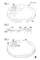
- FIG. 1 we see a wafer 10 of monocrystalline silicon having an upper face 11 on which electronic circuits 12 are formed, by conventional means in microelectronics.
- Each circuit includes at least one regulated current generator and a differential amplifier.
- FIG. 2 shows, in section, the substrate 10, with its circuits 12.
- An insulating layer 14, for example made of SiO2 is deposited on the assembly to isolate the circuits.
- Non-magnetic spacers are formed according to a known technique which is illustrated in FIG. 3. For this, an insulating layer 15 is deposited which is etched to reveal vertical walls where the spacers are to be formed (part a) . The thickness of this layer is at least equal to the width of the track to be read. A layer 16 of non-magnetic material is deposited on the assembly (part b).
- FIG. 4 illustrates the silicon wafer 10 with the integrated circuits 12 and the non-magnetic spacers 20. Naturally, in this figure, the scales are not respected.
- a layer of material is then deposited on the assembly magnetic with high permeability.
- the thickness of this layer is equal to the width of the track to be read.
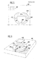
- This layer is etched to give it the shape illustrated in FIG. 5 to form a loop-shaped circuit 30 comprising two pole pieces P1, P2 separated by a spacer 20, and a rear part P3 separated from the pole pieces by two slots F1 and F2 a few micrometers wide.
- This magnetic circuit is close to the integrated circuit 12.
- a thin conductive layer 22 is deposited (dashed in FIG. 2) then spacers are produced as illustrated in FIG. 3.
- a layer of resin is then deposited which is etched according to the shape shown in Figure 5 (the resin remaining outside the hatched area in Figure 5). In the engraved parts, the metal layer is thus released.
- a thin layer of iron-nickel is deposited on the assembly, by sputtering, which is etched so that only thin strips forming magnetoresistors M1 and M2 remain in the slots F1 and F2. As illustrated in FIG. 7, these fine strips are not in electrical contact with the magnetic circuit.
- magnetoresistors instead of magnetoresistors, one could insert into slots F1 and F2, magnetodiodes or magnetotransistors made directly on the silicon substrate.
- a large number of components are thus obtained, each consisting of a magnetic circuit 30 and an integrated circuit 12. These components are cut out and inserted into a flight pad 32, as illustrated in FIG. 9.
- the assembly is carried out by gluing or by welding with glass.
- the complete skate includes a flight plan 34 and is in the form of a catamaran. Tracks 36 and 38 pass under the air gap of each magnetic circuit.
- the face 11, on which the integrated circuit 12 and the magnetic circuit are located, is perpendicular to the flight plane 34 and parallel to the runways 36, 38.
- the width of the track is equal to the thickness of the magnetic layer forming the circuit.
- this width can be very small, and of the order of a micron.
- FIGS. 10 and 11 provide a better understanding of the operation of the read head of the invention, once completed.
- the arrows in the magnetic circuit show the direction of the magnetization during reading and the arrows in the electrical connections the direction of the current flowing through the magnetoresistors. These are moreover polarized by known means which are not shown (self-polarization, "barber poles", etc.).
- This polarization is linked to the reading current and to the magnetization, so that the resistance variation is opposite in the two magnetoresistors, that is to say such that the resistance increases in one of the magnetoresistors then that it decreases in the other, for the same variation of the magnetization.
- FIG. 11 shows the curve of variation of the resistance R of a magnetoresistance as a function of the magnetic field applied.
- Ho the magnetoresistance has a resistance Ro.
- ⁇ H there is a relative variation ⁇ R / Ro for one of the magnetoresistors and - ⁇ R / Ro for the other.
- the current imbalance obtained at the inputs of the differential amplifier is then proportional to 2 ⁇ R / Ro.
- the value of Ho is chosen to correspond to the maximum slope of the curve (inflection point).
Landscapes
- Engineering & Computer Science (AREA)
- Manufacturing & Machinery (AREA)
- Magnetic Heads (AREA)
- Hall/Mr Elements (AREA)
Applications Claiming Priority (2)
| Application Number | Priority Date | Filing Date | Title |
|---|---|---|---|
| FR8703821A FR2612676B1 (fr) | 1987-03-19 | 1987-03-19 | Tete magnetique de lecture pour piste de tres faible largeur et procede de fabrication |
| FR8703821 | 1987-03-19 |
Publications (3)
| Publication Number | Publication Date |
|---|---|
| EP0284495A2 true EP0284495A2 (de) | 1988-09-28 |
| EP0284495A3 EP0284495A3 (en) | 1990-10-31 |
| EP0284495B1 EP0284495B1 (de) | 1993-09-08 |
Family
ID=9349203
Family Applications (1)
| Application Number | Title | Priority Date | Filing Date |
|---|---|---|---|
| EP88400628A Expired - Lifetime EP0284495B1 (de) | 1987-03-19 | 1988-03-16 | Magnetkopf zum Lesen von Spuren mit sehr schmaler Breite und Herstellungverfahren |
Country Status (6)
| Country | Link |
|---|---|
| US (1) | US4901177A (de) |
| EP (1) | EP0284495B1 (de) |
| JP (1) | JPS63255809A (de) |
| DE (1) | DE3883819T2 (de) |
| FR (1) | FR2612676B1 (de) |
| IE (1) | IE63080B1 (de) |
Cited By (2)
| Publication number | Priority date | Publication date | Assignee | Title |
|---|---|---|---|---|
| FR2658647A1 (fr) * | 1990-02-21 | 1991-08-23 | Commissariat Energie Atomique | Tete magnetique horizontale a effet hall et son procede de realisation. |
| US5618738A (en) * | 1994-03-14 | 1997-04-08 | Nippondenso Co., Ltd. | Manufacturing method for magnetoresistance elements |
Families Citing this family (23)
| Publication number | Priority date | Publication date | Assignee | Title |
|---|---|---|---|---|
| FR2645314B1 (fr) * | 1989-03-29 | 1991-05-31 | Commissariat Energie Atomique | Tete magnetique a magnetoresistance pour enregistrement longitudinal et procede de realisation d'une telle tete |
| FR2645315B1 (fr) * | 1989-03-29 | 1991-05-31 | Commissariat Energie Atomique | Tete magnetique de lecture a magnetoresistance pour enregistrement perpendiculaire et procede de realisation d'une telle tete |
| FR2656454B1 (fr) * | 1989-12-22 | 1995-07-21 | Thomson Csf | Tete de lecture multipiste. |
| US5508868A (en) * | 1993-01-25 | 1996-04-16 | Read-Rite Corporation | Dual element magnetoresistive sensing head having in-gap flux guide and flux closure piece with particular connection of magnetoresistive sensing elements to differential amplifier |
| FR2709855B1 (fr) * | 1993-09-06 | 1995-10-20 | Commissariat Energie Atomique | Tête magnétique de lecture et d'écriture à élément magnétorésistant compensé en écriture. |
| CN1067788C (zh) * | 1994-03-07 | 2001-06-27 | 国际商业机器公司 | 制造磁传感器的方法和制造磁盘存储系统的方法 |
| JPH07270507A (ja) * | 1994-03-28 | 1995-10-20 | Sony Corp | 地磁気方位センサ |
| US5673474A (en) * | 1994-08-26 | 1997-10-07 | Aiwa Research And Development, Inc. | Method of fabricating a thin film magnetic head including layered magnetic side poles |
| US6091581A (en) * | 1994-08-26 | 2000-07-18 | Aiwa Co., Ltd. | Thin film magnetic head including a separately deposited diamond-like carbon gap structure and magnetic control wells |
| US5748417A (en) * | 1994-08-26 | 1998-05-05 | Aiwa Research And Development, Inc. | Thin film magnetic head including layered magnetic side poles |
| US5801909A (en) * | 1994-08-26 | 1998-09-01 | Aiwa Research And Development, Inc. | Thin film magnetic head including durable wear layer and non-magnetic gap structures |
| US5544774A (en) * | 1994-08-26 | 1996-08-13 | Aiwa Research And Development, Inc. | Method of eliminating pole recession in a thin film magnetic head |
| US5563754A (en) * | 1994-08-26 | 1996-10-08 | Aiwa Research And Development, Inc. | Thin film magnetic head including a durable wear layer and gap structure |
| US5909346A (en) * | 1994-08-26 | 1999-06-01 | Aiwa Research & Development, Inc. | Thin magnetic film including multiple geometry gap structures on a common substrate |
| US5490028A (en) * | 1994-08-26 | 1996-02-06 | Aiwa Research And Development, Inc. | Thin film magnetic head including an integral layered shield structure |
| JPH08171712A (ja) * | 1994-08-26 | 1996-07-02 | Aiwa Co Ltd | 側面露出型薄膜磁気ヘッド並びにその製造方法 |
| US5754377A (en) * | 1994-08-26 | 1998-05-19 | Aiwa Research And Development, Inc. | Thin film magnetic head including an elevated gap structure |
| US5587857A (en) * | 1994-10-18 | 1996-12-24 | International Business Machines Corporation | Silicon chip with an integrated magnetoresistive head mounted on a slider |
| US5621594A (en) * | 1995-02-17 | 1997-04-15 | Aiwa Research And Development, Inc. | Electroplated thin film conductor coil assembly |
| US6069015A (en) * | 1996-05-20 | 2000-05-30 | Aiwa Research And Development, Inc. | Method of fabricating thin film magnetic head including durable wear layer and non-magnetic gap structure |
| US5768070A (en) * | 1997-05-14 | 1998-06-16 | International Business Machines Corporation | Horizontal thin film write, MR read head |
| EP0889460B1 (de) * | 1997-07-04 | 2003-09-24 | STMicroelectronics S.r.l. | Ein elektromagnetischer Kopf mit magnetoresistiven Mitteln verbunden mit einem Magnetkern |
| US8953284B1 (en) | 2013-11-20 | 2015-02-10 | HGST Netherlands B.V. | Multi-read sensor having a narrow read gap structure |
Family Cites Families (8)
| Publication number | Priority date | Publication date | Assignee | Title |
|---|---|---|---|---|
| DE2205799A1 (de) * | 1972-02-08 | 1973-08-16 | Gehap Gmbh & Co Kg | Fuehler- bzw. tastkopf fuer magnetfeldabhaengige widerstaende |
| US3800193A (en) * | 1972-09-05 | 1974-03-26 | Ibm | Magnetic sensing device |
| JPS5931770B2 (ja) * | 1978-09-19 | 1984-08-04 | 三菱電機株式会社 | 磁気ヘツドのコアの製造方法 |
| US4388662A (en) * | 1981-01-28 | 1983-06-14 | Eastman Kodak Company | Thin film magnetoresistive head |
| JPS5870416A (ja) * | 1981-10-20 | 1983-04-26 | Matsushita Electric Ind Co Ltd | 磁気ヘツドの製造方法 |
| JPS5885916A (ja) * | 1981-11-16 | 1983-05-23 | Akai Electric Co Ltd | 薄膜磁気ヘツドおよびその製造法 |
| US4485419A (en) * | 1982-06-15 | 1984-11-27 | International Business Machines Corporation | Complementary pole coupling magnetic head structure |
| JPS592221A (ja) * | 1982-06-28 | 1984-01-07 | Canon Inc | 薄膜磁気ヘツド |
-
1987
- 1987-03-19 FR FR8703821A patent/FR2612676B1/fr not_active Expired - Fee Related
-
1988
- 1988-03-14 US US07/167,729 patent/US4901177A/en not_active Expired - Fee Related
- 1988-03-16 EP EP88400628A patent/EP0284495B1/de not_active Expired - Lifetime
- 1988-03-16 DE DE88400628T patent/DE3883819T2/de not_active Expired - Fee Related
- 1988-03-17 JP JP63062084A patent/JPS63255809A/ja active Pending
- 1988-03-18 IE IE79588A patent/IE63080B1/en not_active IP Right Cessation
Cited By (4)
| Publication number | Priority date | Publication date | Assignee | Title |
|---|---|---|---|---|
| FR2658647A1 (fr) * | 1990-02-21 | 1991-08-23 | Commissariat Energie Atomique | Tete magnetique horizontale a effet hall et son procede de realisation. |
| EP0443941A1 (de) * | 1990-02-21 | 1991-08-28 | Commissariat A L'energie Atomique | Horizontaler Magnetkopf mit Halleffekt und sein Herstellungsverfahren |
| US5166849A (en) * | 1990-02-21 | 1992-11-24 | Commissariat A L'energie Atomique | Horizontal magnetic head with hall effect and its embodiment method |
| US5618738A (en) * | 1994-03-14 | 1997-04-08 | Nippondenso Co., Ltd. | Manufacturing method for magnetoresistance elements |
Also Published As
| Publication number | Publication date |
|---|---|
| EP0284495B1 (de) | 1993-09-08 |
| JPS63255809A (ja) | 1988-10-24 |
| US4901177A (en) | 1990-02-13 |
| EP0284495A3 (en) | 1990-10-31 |
| FR2612676A1 (fr) | 1988-09-23 |
| IE880795L (en) | 1988-09-19 |
| DE3883819D1 (de) | 1993-10-14 |
| FR2612676B1 (fr) | 1993-12-31 |
| IE63080B1 (en) | 1995-03-22 |
| DE3883819T2 (de) | 1994-03-17 |
Similar Documents
| Publication | Publication Date | Title |
|---|---|---|
| EP0284495B1 (de) | Magnetkopf zum Lesen von Spuren mit sehr schmaler Breite und Herstellungverfahren | |
| EP0418372B1 (de) | Lese-magnetkopf mit magnetowiderstand für senkrechte aufzeichnung und herstellungsverfahren eines derartigen kopfes | |
| EP0417261B1 (de) | Magnetkopf mit magnetowiderstand für longitudinale aufzeichnung und herstellungsverfahren eines derartigen kopfes | |
| EP0420755B1 (de) | Herstellungsverfahren eines Magnetaufzeichnungskopfes und nach diesem Verfahren erhaltener Kopf | |
| EP0652550B1 (de) | Lesemagnetkopf mit Mehrschichtmagnetowiderstandselement und Konzentrator und Herstellungsverfahren | |
| FR2605783A1 (fr) | T ete magnetique d'enregistrement/lecture en couches minces et son procede de realisation | |
| FR2726931A1 (fr) | Tete magnetique verticale a bobinage integre et son procede de realisation | |
| EP0046697B1 (de) | Integrierter Magnetwandler | |
| EP0702358A1 (de) | Magnetkopf mit unterliegendem longitudinalem Mehrschicht-Magnetowiderstand | |
| EP0781448B1 (de) | Planarer magnetkopf mit longitudinalem mehrschichtmagnetowiderstand | |
| EP0642030A1 (de) | Flussleiter mit Zungen und magnetischer Sensor mit einem solchen Flussleiter | |
| EP0642181A1 (de) | Magnetoresistive Anordnung und Fühler mit wiederholenden geometrischen Strukturen | |
| EP0040994B1 (de) | Magnetwandler, der einen Spalt mit veränderbarer Grössen-Dimension aufweist, zur Wiedergabe oder zum Aufzeichnen von Informationen eines magnetischen Trägers | |
| EP0497069B1 (de) | Herstellungsverfahren von magnetoresistiven Sensoren und nach diesem Verfahren hergestellte magnetische Vorrichtung | |
| EP0644528B1 (de) | Aufzeichnungs- und Wiedergabemagnetkopf mit bezüglich Aufzeichnung kompensiertem Magnetowiderstandselement | |
| EP0800160B1 (de) | Herstellungsverfahren für einen Doppel-Magnetkopf mit entgegengesetzten Azimuth-Spalten | |
| EP0266266A1 (de) | Verfahren zur Herstellung einer plattenförmigen gewickelten magnetischen Lese- und -Wiedergabekopfanordnung und eine Kopfanordnung durch dieses Verfahren hergestellt | |
| EP0694909A1 (de) | Magnetkopf mit sättigbarem Element und Matrixanordnung bestehend aus einem Satz von Magnetköpfen | |
| FR2496952A1 (fr) | Tete de transducteur magnetique a effet de magneto-resistance | |
| EP1107236A1 (de) | Flacher Magnetkopf mit magnetoresistivem Element | |
| FR2713782A1 (fr) | Capteur magnétique à effet magnéto-résistif. | |
| FR2676301A1 (fr) | Tete magnetique d'ecriture et de lecture a largeur de poles dissymetrique. | |
| FR2769399A1 (fr) | Tete magnetique avec une partie lecture et une partie ecriture | |
| JP2000020914A (ja) | 金属膜形成方法及び薄膜磁気ヘッドのポール形成方法 | |
| EP0669609B1 (de) | Lesemagnetkopf mit magnetoresistivem Element und verbesserten Vormagnetisierungsmitteln |
Legal Events
| Date | Code | Title | Description |
|---|---|---|---|
| PUAI | Public reference made under article 153(3) epc to a published international application that has entered the european phase |
Free format text: ORIGINAL CODE: 0009012 |
|
| AK | Designated contracting states |
Kind code of ref document: A2 Designated state(s): BE CH DE GB IT LI NL |
|
| PUAL | Search report despatched |
Free format text: ORIGINAL CODE: 0009013 |
|
| AK | Designated contracting states |
Kind code of ref document: A3 Designated state(s): BE CH DE GB IT LI NL |
|
| 17P | Request for examination filed |
Effective date: 19910404 |
|
| 17Q | First examination report despatched |
Effective date: 19920309 |
|
| GRAA | (expected) grant |
Free format text: ORIGINAL CODE: 0009210 |
|
| AK | Designated contracting states |
Kind code of ref document: B1 Designated state(s): BE CH DE GB IT LI NL |
|
| PG25 | Lapsed in a contracting state [announced via postgrant information from national office to epo] |
Ref country code: IT Free format text: LAPSE BECAUSE OF FAILURE TO SUBMIT A TRANSLATION OF THE DESCRIPTION OR TO PAY THE FEE WITHIN THE PRE;WARNING: LAPSES OF ITALIAN PATENTS WITH EFFECTIVE DATE BEFORE 2007 MAY HAVE OCCURRED AT ANY TIME BEFORE 2007. THE CORRECT EFFECTIVE DATE MAY BE DIFFERENT FROM THE ONE RECORDED.SCRIBED TIME-LIMIT Effective date: 19930908 |
|
| REF | Corresponds to: |
Ref document number: 3883819 Country of ref document: DE Date of ref document: 19931014 |
|
| GBT | Gb: translation of ep patent filed (gb section 77(6)(a)/1977) |
Effective date: 19931122 |
|
| PLBE | No opposition filed within time limit |
Free format text: ORIGINAL CODE: 0009261 |
|
| STAA | Information on the status of an ep patent application or granted ep patent |
Free format text: STATUS: NO OPPOSITION FILED WITHIN TIME LIMIT |
|
| 26N | No opposition filed | ||
| PGFP | Annual fee paid to national office [announced via postgrant information from national office to epo] |
Ref country code: BE Payment date: 19970228 Year of fee payment: 10 |
|
| PGFP | Annual fee paid to national office [announced via postgrant information from national office to epo] |
Ref country code: CH Payment date: 19970314 Year of fee payment: 10 |
|
| PGFP | Annual fee paid to national office [announced via postgrant information from national office to epo] |
Ref country code: NL Payment date: 19970331 Year of fee payment: 10 |
|
| PGFP | Annual fee paid to national office [announced via postgrant information from national office to epo] |
Ref country code: GB Payment date: 19980304 Year of fee payment: 11 |
|
| PGFP | Annual fee paid to national office [announced via postgrant information from national office to epo] |
Ref country code: DE Payment date: 19980316 Year of fee payment: 11 |
|
| PG25 | Lapsed in a contracting state [announced via postgrant information from national office to epo] |
Ref country code: CH Free format text: LAPSE BECAUSE OF NON-PAYMENT OF DUE FEES Effective date: 19980331 Ref country code: BE Free format text: LAPSE BECAUSE OF NON-PAYMENT OF DUE FEES Effective date: 19980331 Ref country code: LI Free format text: LAPSE BECAUSE OF NON-PAYMENT OF DUE FEES Effective date: 19980331 |
|
| BERE | Be: lapsed |
Owner name: COMMISSARIAT A L'ENERGIE ATOMIQUE Effective date: 19980331 |
|
| PG25 | Lapsed in a contracting state [announced via postgrant information from national office to epo] |
Ref country code: NL Free format text: LAPSE BECAUSE OF NON-PAYMENT OF DUE FEES Effective date: 19981001 |
|
| REG | Reference to a national code |
Ref country code: CH Ref legal event code: PL |
|
| NLV4 | Nl: lapsed or anulled due to non-payment of the annual fee |
Effective date: 19981001 |
|
| PG25 | Lapsed in a contracting state [announced via postgrant information from national office to epo] |
Ref country code: GB Free format text: LAPSE BECAUSE OF NON-PAYMENT OF DUE FEES Effective date: 19990316 |
|
| GBPC | Gb: european patent ceased through non-payment of renewal fee |
Effective date: 19990316 |
|
| PG25 | Lapsed in a contracting state [announced via postgrant information from national office to epo] |
Ref country code: DE Free format text: LAPSE BECAUSE OF NON-PAYMENT OF DUE FEES Effective date: 20000101 |