EP0284724A2 - Equipement de mémoire permanente à semi-conducteur - Google Patents
Equipement de mémoire permanente à semi-conducteur Download PDFInfo
- Publication number
- EP0284724A2 EP0284724A2 EP88101336A EP88101336A EP0284724A2 EP 0284724 A2 EP0284724 A2 EP 0284724A2 EP 88101336 A EP88101336 A EP 88101336A EP 88101336 A EP88101336 A EP 88101336A EP 0284724 A2 EP0284724 A2 EP 0284724A2
- Authority
- EP
- European Patent Office
- Prior art keywords
- voltage
- read
- line layer
- write
- memory device
- Prior art date
- Legal status (The legal status is an assumption and is not a legal conclusion. Google has not performed a legal analysis and makes no representation as to the accuracy of the status listed.)
- Granted
Links
- 239000004065 semiconductor Substances 0.000 title claims abstract description 32
- 238000009792 diffusion process Methods 0.000 claims description 80
- 239000000758 substrate Substances 0.000 claims description 10
- 230000005684 electric field Effects 0.000 description 11
- 238000012986 modification Methods 0.000 description 11
- 230000004048 modification Effects 0.000 description 11
- 238000010586 diagram Methods 0.000 description 9
- 229910021420 polycrystalline silicon Inorganic materials 0.000 description 7
- 229920005591 polysilicon Polymers 0.000 description 6
- 230000007423 decrease Effects 0.000 description 4
- 238000002347 injection Methods 0.000 description 4
- 239000007924 injection Substances 0.000 description 4
- 229920000136 polysorbate Polymers 0.000 description 3
- 230000003247 decreasing effect Effects 0.000 description 2
- 230000000694 effects Effects 0.000 description 2
- 230000002093 peripheral effect Effects 0.000 description 2
- 230000003334 potential effect Effects 0.000 description 2
- 241001663154 Electron Species 0.000 description 1
- 238000010276 construction Methods 0.000 description 1
- 230000014759 maintenance of location Effects 0.000 description 1
- 238000004519 manufacturing process Methods 0.000 description 1
Images



Classifications
-
- H—ELECTRICITY
- H10—SEMICONDUCTOR DEVICES; ELECTRIC SOLID-STATE DEVICES NOT OTHERWISE PROVIDED FOR
- H10B—ELECTRONIC MEMORY DEVICES
- H10B69/00—Erasable-and-programmable ROM [EPROM] devices not provided for in groups H10B41/00 - H10B63/00, e.g. ultraviolet erasable-and-programmable ROM [UVEPROM] devices
-
- G—PHYSICS
- G11—INFORMATION STORAGE
- G11C—STATIC STORES
- G11C16/00—Erasable programmable read-only memories
- G11C16/02—Erasable programmable read-only memories electrically programmable
- G11C16/04—Erasable programmable read-only memories electrically programmable using variable threshold transistors, e.g. FAMOS
- G11C16/0408—Erasable programmable read-only memories electrically programmable using variable threshold transistors, e.g. FAMOS comprising cells containing floating gate transistors
- G11C16/0433—Erasable programmable read-only memories electrically programmable using variable threshold transistors, e.g. FAMOS comprising cells containing floating gate transistors comprising cells containing a single floating gate transistor and one or more separate select transistors
-
- G—PHYSICS
- G11—INFORMATION STORAGE
- G11C—STATIC STORES
- G11C16/00—Erasable programmable read-only memories
- G11C16/02—Erasable programmable read-only memories electrically programmable
- G11C16/06—Auxiliary circuits, e.g. for writing into memory
- G11C16/10—Programming or data input circuits
- G11C16/12—Programming voltage switching circuits
-
- G—PHYSICS
- G11—INFORMATION STORAGE
- G11C—STATIC STORES
- G11C16/00—Erasable programmable read-only memories
- G11C16/02—Erasable programmable read-only memories electrically programmable
- G11C16/06—Auxiliary circuits, e.g. for writing into memory
- G11C16/10—Programming or data input circuits
- G11C16/14—Circuits for erasing electrically, e.g. erase voltage switching circuits
-
- G—PHYSICS
- G11—INFORMATION STORAGE
- G11C—STATIC STORES
- G11C16/00—Erasable programmable read-only memories
- G11C16/02—Erasable programmable read-only memories electrically programmable
- G11C16/06—Auxiliary circuits, e.g. for writing into memory
- G11C16/26—Sensing or reading circuits; Data output circuits
-
- H—ELECTRICITY
- H10—SEMICONDUCTOR DEVICES; ELECTRIC SOLID-STATE DEVICES NOT OTHERWISE PROVIDED FOR
- H10D—INORGANIC ELECTRIC SEMICONDUCTOR DEVICES
- H10D30/00—Field-effect transistors [FET]
- H10D30/60—Insulated-gate field-effect transistors [IGFET]
- H10D30/68—Floating-gate IGFETs
Definitions
- This invention relates to a nonvolatile semiconductor memory device comprising a nonvolatile transistor and allowing the stored data to be replaced by another data.
- E2ROM electrically erasable and programmable read only memory
- One known memory cell for use in the E2PROM is a floating gate type memory cell, in which the floating gate electrode partially overlaps a thin insulating film formed on the diffusion layer.
- Fig. 1 is a sectional view showing the structure of a prior art memory cell of this type.
- N type diffusion layers 41, 42 and 43 are formed in the surface region of P type semiconductor substrate 40.
- Channel region 44 is formed between diffusion layers 41 and 42.
- a relatively thick insulating film 45 is formed on channel region 44.
- Electrode 46 made of polysilicon is formed on the insulating layer 45. Electrode 46 extends over N type diffusion layer 42. A portion of electrode 46 projects toward diffusion layer 42. Insulating film 47 exists between diffusion layer 42 and a portion of electrode 46. Insulating film 47 is thinner insulating film 45.
- Insulating film 48 is formed on electrode 46.
- Electrode 49 made of polysilicon is formed on insulating film 48.
- Channel region 50 is also formed between diffusion layers 42 and 43. Relatively thick insulating film 51 is formed on channel region 50. Further, electrode 52 made of polysilicon is formed on insulating film 51.
- Source interconnection S is connected to diffusion layer 41, and bit line BL is connected to diffusion layer 43.
- Electrode 46 is used as a floating gate electrode, and electrode 49 is used as a control gate electrode, and electrode 52 is used as gate electrode.
- Control gate electrode 49 is connected to control gate wire CG, and select gate wire SG is connected to gate electrode 52.
- Fig. 2 shows an equivalent circuit of the prior art memory cell shown in Fig. 1.
- transistor 61 is of the floating gate type in which diffusion layers 41 and 42 are a source and a drain, respectively. This transistor constitutes a memory transistor for storing data.
- Transistor 62 is of the MOS type in which diffusion layers 42 and 43 are a source and a drain, respectively. This transistor is for selecting memory transistor 61.
- Operation modes of such memory cells includes a data-erase mode, a data-write mode and a data-read mode.
- Fig. 3 tabulates the voltages applied to source interconnection S, bit line BL, control gate wire CG, and selecting gate wire SG.
- Power source voltage Vpp is not supplied from an external power supply, but formed by increasing the Vcc voltage in the IC circuit.
- the data-erase mode will first be described.
- This mode is also called an electron injection mode.
- electrons are injected into floating gate electrode 46 to increase the threshold voltage V TH of memory transistor 61.
- BL 0 V
- SG 20 V
- CG 20 V
- S 0 V.
- selecting transistor 62 is turned on, and the potential at N type diffusion layer 42 becomes to the BL potential, i.e., 0 V.
- Floating gate electrode 46 is coupled with a high voltage of CG, 20 V. Under this condition, a high electric field is applied to thin insulating film 47 formed between floating gate electrode 46 and N type diffusion layer 42. Consequently, floating gate electrode 46 is injected with electrons from N type diffusion layer 42 by a tunnel current.
- the threshold voltage V TH of memory transistor 32 increases to, for example, + 8 V.
- the data-write mode is called an electron-emission mode in which electrons injected into floating gate electrode 46 are discharged therefrom to decrease the threshold voltage V TH of memory transistor 61.
- BL 20 V
- SG 20 V
- CG 0 V
- S 5 V.
- selecting transistor 62 is turned on, and N type diffusion layer 42 becomes to the BL potential, i.e., 20 V. Therefore, a high electric field whose direction is opposite to that of the erase mode, is applied to thin insulating film 47. Consequently, the electrons is discharged from floating gate electrode 46 to N type diffusion layer 42.
- the threshold voltage V TH of memory transistor 61 decreases to, for example, - 5 V.
- BL 1 V
- SG 5 V
- CG 0 V
- S 0 V.
- N type diffusion layer 42 becomes to the BL potential, i.e., 1 V.
- memory transistor 61 is kept to be turned off. No current flows through BL and S, and BL is kept at 1 V.
- electrons have been emitted from floating gate electrode 46
- the threshold voltage of memory transistor 61 has been descreased.
- transistor 61 is turned on. At this time, a current flows from floating gate electrode 46 toward N type diffusion layer 42, and the potential of BL becomes to the S potential, i.e., approximately 0 V. A potential difference between 1 V and 0 V on bit line BL is amplified by a sense amplifier (not shown) connected to bit line BL, to determine a logical "1" or a logical "0".
- the electric fields in the read and write modes are compared, the directions of the electric fields are the same, but the intensities are different. The electric field intensity in the read mode is lower than that in the write mode.
- bit line potential in the read mode is limited to about 1 V.
- a first problem resides in the complicated circuit of the sense amplifier. To fabricate such a complicated amplifier circuit into a semiconductor chip, a large area is required on the semiconductor chip, resulting in increase of cost of manufacture.
- a second problem resides in the reduced margin for the power source voltage in the read mode. This is undesirable for the low voltage operation.
- a third problem resides in the need for the constant voltage source of 1 V (intermediate voltage) to be supplied to the bit line.
- the prior art memory device must comprise a circuit for forming such an intermediate voltage, resulting in increase of power consumption.
- a fourth problem resides in a long access time due to the complicated structure of the sense amplifier.
- the prior art nonvolatile memory device involves many problems; the large area required on the semiconductor chip, instable low voltage operation, large power consumption, and the long access time.
- an object of this invention is to provide a nonvolatile memory device which is featured by low operation voltage, low power consumption, high operating speed, and the simple periphery circuitry including the sense amplifier.
- a nonvolatile semiconductor memory device comprising: a write line layer; a read line layer; a write gate line layer; a control gate line layer; a read gate line layer; a cell transistor formed of a floating gate type MOS transistor, for storing an electric charge, whose gate is connected to said control gate line layer; a first selecting transistor formed of an MOS transistor, whose gate is connected to said read gate line layer, one terminal of whose source-drain path is connected to said read line layer, and the other terminal of the source-drain path is connected to one terminal of the source-drain path of said cell transistor; and a second selecting transistor formed of an MOS transistor, whose gate is connected to said write gate line layer, one terminal of whose source-drain path is connected to said write line layer, and the other terminal of the source-drain path is connected to the other terminal of said source-drain path of said cell transistor.
- a nonvolatile semiconductor memory device comprising: a semiconductor substrate of a first conductivity type; first to fourth diffusion layers of a second conductivity type formed in said substrate; a first channel region formed between said first and second diffusion layers; a second channel region formed between said second and third diffusion layers; a third channel region formed between said third and fourth diffusion layers; a first gate electrode formed above said first channel region; a floating gate electrode formed above said second channel region, and extending above said third diffusion layer; a control gate electrode formed above said floating gate electrode; a second gate electrode formed above said third channel region; a first insulating layer formed between said second channel region and said floating gate electrode; a second insulating layer formed between said third diffusion layer and said extending portion of said floating gate electrode, the second insulating layer having a thickness thinner than that of said first insulating layer; a write line layer for supplying a predetermined voltage to said fourth diffusion layer in data erase, write, and read modes; a write gate line layer for supplying a
- a nonvolatile semiconductor memory device comprising: a semiconductor substrate of a first conductivity type; first to third diffusion layers of a second conductivity type formed in said substrate; first and second channel regions formed in series between said first and second diffusion layers; a third channel region formed between said second and third diffusion layers; a first gate electrode formed above said first channel region; a floating gate electrode formed above said second channel region, and extending above said second diffusion layer; a control gate electrode formed above said floating gate electrode; a second gate electrode formed above said third channel region; a first insulating layer formed between said second channel region and said floating gate electrode; a second insulating layer formed between said third diffusion layer and said extending portion of said floating gate electrode, the second insulating layer having a thickness thinner than that of said first insulating layer; a write line layer for supplying a predetermined voltage to said third diffusion layer in data erase, write and read modes; a write gate line layer for supplying a predetermined voltage to
- a memory cell used in a nonvolatile semiconductor memory device is shown in Fig. 4.
- N type diffusion layers 11, 12, 13, and 14 are formed in the surface region of P type semiconductor substrate 10.
- Channel region 15 is formed between diffusion layers 11 and 12.
- Relatively thick insulating film 16 is formed on channel region 15.
- Electrode 17 made of polysilicon is formed on insulating film 16.
- Channel region 18 is formed between diffusion layer 12 and 13.
- Relatively thick insulating film 19 is also formed on channel region 18.
- Electrode 20 made of polysilicon is formed on insulating film 19.
- Electrode 20 extends over N type diffusion layer 13.
- a portion of extended electrode 20 projects toward diffusion layer 13.
- Insulating film 21 exists between diffusion layer 13 and the projected portion of extended electrode 20.
- the thickness of insulating film 21 is thinner than that of insulating film 19.
- the projected portion of extended electrode 20 is formed on insulating film 21.
- Insulating film 22 is formed on electrode 20.
- Electrode 23 made of polysilicon
- Channel region 24 is formed between diffusion layers 13 and 14. Relatively thick insulating film 25 is also formed on channel region 24. Electrode 26 made of polysilicon is formed on insulating film.
- Read line RL is connected to diffusion layer 11, and write line WL is connected to diffusion layer 14.
- Electrodes 17 and 26 are used as gate electrodes; electrode 20 is used as a floating gate electrode; electrode 23 is used as a control gate electrode.
- Gate electrode 17 is connected to read gate line RG; control gate electrode 23 is connected to control gate line CG; gate electrode 26 is connected to gate line WG.
- Fig. 5 shows an equivalent circuit of the cell of Fig. 4.
- transistor 31 is of MOS type, in which diffusion layers 11 and 12 are used as a source and a drain, respectively.
- This transistor is a first selecting transistor for selecting a memory transistor.
- Transistor 32 is of floating gate type, in which diffusion layers 12 and 13 are used as a source and a drain, respectively.
- This transistor is the memory transistor for storing data therein.
- Transistor 33 is of MOS type, in which diffusion layers 13 and 14 are used as a source and a drain, respectively. This transistor serves as a second selecting transistor.
- Operation modes of the memory cell of such structure includes data erase mode, data write mode, and data read mode, as in the case of the conventional memory cell.
- Fig. 6 tabulates the voltages supplied to read line WL, write gate line WG, control gate line CG, read gate line RG, and read line RL.
- any value of voltage may be set at read line RL.
- second selecting transistor 33 is turned on, so that N type diffusion layer 13 is at the WL potential, i.e., 0 V.
- the high voltage supplied to CG, i.e., 20 V, is applied to floating gate electrode 20.
- first selecting transistor 31 is turned off, and N type diffusion layer 12 is electrically in the floating state.
- threshold voltage V TH of memory transistor 32 increases to, for example, + 8 V.
- the voltage supplied to read line RL may be set to any value.
- second selecting transistor 33 is turned on, so that N type diffusion layer 13 is at the WL potential, i.e., 20 V.
- a high electric field whose direction is opposite to that in the erase mode is applied to thin insulating film 21.
- the electric field causes a tunnel current to flow, to discharge the electrons from floating gate electrode 20 to N type diffusion layered 13.
- threshold voltage V TH of memory transistor 32 decreases to, for example, - 5 V.
- the basic operations of the erase mode and the read modes are substantially the same as those in the conventional memory cell.
- WL 0 V
- WG 5 V
- CG 0 V
- RG 5 V
- RL 5 V
- first and second selecting transistors 31 and 32 are turned on, and the potential of N type diffusion layer 12 is the RL potential, i.e., 5 V
- that of diffusion layer 13 is the potential of WL, 0 V.
- threshold voltage V TH has been increased
- memory transistor 32 is not turned on. Accordingly, there is no current flow through read lines RL and WL, and RL is held at 5 V.
- threshold voltage V TH has been decreased, and memory transistor 32 is turned on. At this time, there is a current flow through read lines RL and WL, and RL becomes to the WL potential, i.e., approximately 0 V. A potential difference between 5 V and 0 V on read line RL is amplified by a sense amplifier (not shown), to determine a logical "1" or a logical "0".
- the power source voltage of 5 V used can be supplied to read line RL in the read mode. It is further noted that even when the 5 V voltage is supplied to read line RL, the read retention characteristic can be remarkably improved, while suppressing the soft write phenomenon.
- Fig. 7 schematically shows a circuit diagram of E2PROM device to which the nonvolatile semiconductor memory cell shown Figs. 4 and 5 is applied. In this figure, only one memory cell is shown for simplicity of illustration.
- the memory cell has first and second selecting transistors 31 and 32 and memory transistor 32.
- Resistor 34 as a load circuit is connected between read line RL and reading power source source Vcc.
- Read line RL is connected to the input terminal of sense amplifier 35.
- resistance of resistor 34 is Rr
- resistance between RL and WL taken when electrons are charged into memory cell 32 is Roff
- resistance between RL and WL taken when electrons are discharged from is Ron.
- resistance Rr is selected as given below Roff » Rr » Ron ...
- the voltage on read line RL is 5 V or 0 V depending on the electron injection or electron emission to or from memory cell 32. That is to say, the voltage on read line RL fully swings between 5 V and 0 V. Thus, if power source voltage Vcc is decreased, a satisfactory operation margin can be secured for the low voltage operation. Furthermore, the memory device of this invention does not require an intermediate voltage of 1 V, and hence, does not require a circuit for generating such voltage.
- the voltage ranges are: 0 V to 20 V (high voltage system) for WL, 5 V to 20 V (low and high voltage systems) for WG, 0 V to 20 V (high voltage system) for CG, 0 V to 5 V (low voltage system) of RG, and and 0 V to 5 V (low voltage system) for RL.
- Only WG uses both high voltage system and low voltage systems.
- the periphery circuits for processing these signals are simple. In short, the peripheral circuits can be separated between the high voltage system and the low voltage system, simplifying the circuit arrangement.
- Fig. 8 schematically shows a circuit diagram of another embodiment of a semiconductor memory device according to this invention.
- P channel MOS transistor 36 is used as the load circuit of read line RL. Ground is connected to the gate electrode, so that transistor 36 is kept turned on.
- Rr conduction resistance of transistor 36
- the value of resistance Rr is selected so as to satisfy the relation (1).
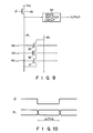
- Fig. 9 shows yet another embodiment of a semiconductor memory device according to this invention.
- P channel MOS transistor 36 is used as the load circuit of read line RL.
- the gate electrode of transistor 36 is supplied with clock signal ⁇ .
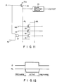
- Fig. 11 shows a circuit diagram showing an arrangement of a further embodiment of this invention.
- P channel MOS transistor 36 used as a load circuit of read line RL is coupled at the gate with clock signal ⁇ .
- the voltage of RG is applied not directly to, but via AND gate 37, to the gate electrode of transistor 31, under control of clock signal ⁇ .
- Fig. 12 shows a timing chart for explaining the operation of the memory device shown in Fig. 11.
- ⁇ 0 V
- P channel MOS transistor 36 is turned on to precharge RL at Vcc.
- the output of AND gate 37 is at 0 V. Therefore, the first selecting transistor 31 supplied with an output of AND gate 37 is turned off, and thus, there is no current path routed from RL to the memory cell to WL.
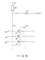
- Fig. 13 shows a circuit diagram of a memory device in which a sense amplifier is formed of an inverter.
- the load circuit 38 of read line RL may be formed of resistor 34 in Fig. 7, P channel MOS transistor 36 in Fig. 8 set in an normally-conductive state, P channel MOS transistor 36 controlled by clock signal ⁇ , or the like.
- the voltage of RL fully swings between 0 V and 5 V.
- an inverter can be used as sense amplifier 35, as shown in Fig. 13. The result is simplification of the sense amplifier and reduction of the access time.
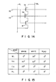
- Fig.14 shows an equivalent circuit of a memory cell, which is a modification of this the memory cell shown in Fig. 4.
- theegate electrodes of first and second selecting transistors 31 and 33 are interconnected, the common gate electrode is connected to selecting gate line SG.
- this connection arrangement is substantially the same as that of the circuit of Fig. 5, except that the write gate line and the read gate line are interconnected and the interconnected line is used as selecting gate line SG. Therefore, this memory cell of Fig. 14 can be applied to the semiconductor devices shown in Fig. 7, 8, 9, 11, or 13.
- Fig. 15 shows a table denoting the voltages supplied to write line WL, selecting gate line SG, control gate line CG, and read line RL in the respective modes of the memory cell shown in Fig. 4.
- the voltages of supplied to selecting gate line SG are the same as those of write gate line WG in Fig. 6.
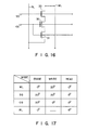
- Fig. 16 shows an equivalent circuit of a memory cell according to a second modification of the memory cell shown in Fig. 4.
- the gate electrode of first select transistor 31 and the control gate electrode of memory transistor 32 are interconnected, and the interconnected electrode is connected to control gate line CG.
- this connection arrangement is substantially the same as that of the circuit of Fig. 5, except that the read gate line and control gate line CG are interconnected and the interconnected line is used as a common gate line CG.
- Fig. 17 shows a table denoting the voltages supplied to write line WL, selecting gate line SG, control gate line CG, and read line RL in the respective modes of the memory cell shown in Fig. 16.
- First selecting transistor 31 is turned on in the data erase mode according to the CG voltage. However, if the voltage of RL is set to 0 V, no current flows through the source and drain of memory transistor 32, and no problem arises.
- Fig. 18 shows a cross sectional view of a memory cell according to a further modification of the memory cell shown in Fig. 4.
- N type diffusion layer 12 is formed between channel regions 15 and 18.
- no layer corresponding to the N type diffusion layer 12 is formed.
- channel regions 15 and 18 are formed in a series form between N type diffusion layers 11 and 13.
- the equivalent circuit of the memory cell having such structure is the same as that of the memory cell shown in Fig. 5. Therefore, it is possible to construct the memory devices shown by the equivalent circuits in Figs. 7 to 9, and 11, by using the memory cell shown in Fig. 18. Further, the memory devices may be further modified as shown in Fig. 14 or 16.
- Fig. 19 shows a cross sectional view of a memory cell according to a still further modification of the memory cell shown in Fig. 4.
- a common layer is used for both the gate electrode formed above channel region 15 and control gate electrode 23, and the common electrode is used as control gate electrode 23.
- the equivalent circuit of this memory cell shown in Fig. 19 is the same as that shown in Fig. 16.
- the semiconductor memory device With such arrangements of the semiconductor memory device, a low operation voltage and a low power dissipation are realized. Further, the peripheral circuits including the sense amplifier are simplified in construction, and operable at a high speed.
Landscapes
- Engineering & Computer Science (AREA)
- Microelectronics & Electronic Packaging (AREA)
- Non-Volatile Memory (AREA)
- Read Only Memory (AREA)
- Semiconductor Memories (AREA)
Priority Applications (1)
| Application Number | Priority Date | Filing Date | Title |
|---|---|---|---|
| EP91104554A EP0440265B1 (fr) | 1987-01-31 | 1988-01-29 | Equipement de mémoire permanente à semi-conducteur |
Applications Claiming Priority (2)
| Application Number | Priority Date | Filing Date | Title |
|---|---|---|---|
| JP21088/87 | 1987-01-31 | ||
| JP2108887A JPH0777078B2 (ja) | 1987-01-31 | 1987-01-31 | 不揮発性半導体メモリ |
Related Child Applications (2)
| Application Number | Title | Priority Date | Filing Date |
|---|---|---|---|
| EP91104554A Division EP0440265B1 (fr) | 1987-01-31 | 1988-01-29 | Equipement de mémoire permanente à semi-conducteur |
| EP91104554.0 Division-Into | 1988-01-29 |
Publications (3)
| Publication Number | Publication Date |
|---|---|
| EP0284724A2 true EP0284724A2 (fr) | 1988-10-05 |
| EP0284724A3 EP0284724A3 (en) | 1989-03-08 |
| EP0284724B1 EP0284724B1 (fr) | 1992-11-11 |
Family
ID=12045117
Family Applications (2)
| Application Number | Title | Priority Date | Filing Date |
|---|---|---|---|
| EP88101336A Expired - Lifetime EP0284724B1 (fr) | 1987-01-31 | 1988-01-29 | Equipement de mémoire permanente à semi-conducteur |
| EP91104554A Expired - Lifetime EP0440265B1 (fr) | 1987-01-31 | 1988-01-29 | Equipement de mémoire permanente à semi-conducteur |
Family Applications After (1)
| Application Number | Title | Priority Date | Filing Date |
|---|---|---|---|
| EP91104554A Expired - Lifetime EP0440265B1 (fr) | 1987-01-31 | 1988-01-29 | Equipement de mémoire permanente à semi-conducteur |
Country Status (5)
| Country | Link |
|---|---|
| US (1) | US4870615A (fr) |
| EP (2) | EP0284724B1 (fr) |
| JP (1) | JPH0777078B2 (fr) |
| KR (1) | KR910000918B1 (fr) |
| DE (2) | DE3875767T2 (fr) |
Cited By (6)
| Publication number | Priority date | Publication date | Assignee | Title |
|---|---|---|---|---|
| EP0394705A1 (fr) * | 1989-03-31 | 1990-10-31 | Oki Electric Industry Co., Ltd. | Système de mémoire non volatile pour mémorisation de valeur multiple |
| US5051796A (en) * | 1988-11-10 | 1991-09-24 | Texas Instruments Incorporated | Cross-point contact-free array with a high-density floating-gate structure |
| EP0426282A3 (en) * | 1989-10-31 | 1992-05-13 | Sgs-Thomson Microelectronics, Inc. | Three transistor eeprom cell |
| US5238855A (en) * | 1988-11-10 | 1993-08-24 | Texas Instruments Incorporated | Cross-point contact-free array with a high-density floating-gate structure |
| EP0676811A1 (fr) * | 1994-04-11 | 1995-10-11 | Motorola, Inc. | Cellule EEPROM avec transistor d'isolation et procédés pour sa fabrication et son fonctionnement |
| EP0757835A4 (fr) * | 1994-04-29 | 1996-11-22 | Atmel Corp | Cellule memoire remanente a haute vitesse, electriquement programmable et effa able, et procede |
Families Citing this family (26)
| Publication number | Priority date | Publication date | Assignee | Title |
|---|---|---|---|---|
| JP2645585B2 (ja) * | 1989-03-10 | 1997-08-25 | 工業技術院長 | 半導体不揮発性メモリ及びその書き込み方法 |
| JPS63252481A (ja) * | 1987-04-09 | 1988-10-19 | Toshiba Corp | 不揮発性半導体メモリ |
| JPH0738274B2 (ja) * | 1988-12-22 | 1995-04-26 | 株式会社東芝 | 不揮発性半導体メモリシステム |
| JP2537413B2 (ja) * | 1989-03-14 | 1996-09-25 | 三菱電機株式会社 | 半導体装置およびその製造方法 |
| US5065362A (en) * | 1989-06-02 | 1991-11-12 | Simtek Corporation | Non-volatile ram with integrated compact static ram load configuration |
| US5283758A (en) * | 1989-06-13 | 1994-02-01 | Mitsubishi Denki Kabushiki Kaisha | Non-volatile semiconductor memory device |
| US5355007A (en) * | 1990-11-23 | 1994-10-11 | Texas Instruments Incorporated | Devices for non-volatile memory, systems and methods |
| US5331590A (en) * | 1991-10-15 | 1994-07-19 | Lattice Semiconductor Corporation | Single poly EE cell with separate read/write paths and reduced product term coupling |
| KR930011000A (ko) * | 1991-11-29 | 1993-06-23 | 김광호 | 이이피롬 장치 |
| JP3293893B2 (ja) * | 1991-12-09 | 2002-06-17 | 株式会社東芝 | 半導体不揮発性記憶装置の製造方法 |
| US5793081A (en) * | 1994-03-25 | 1998-08-11 | Nippon Steel Corporation | Nonvolatile semiconductor storage device and method of manufacturing |
| US5550072A (en) * | 1994-08-30 | 1996-08-27 | National Semiconductor Corporation | Method of fabrication of integrated circuit chip containing EEPROM and capacitor |
| JP3457106B2 (ja) * | 1995-10-13 | 2003-10-14 | ローム株式会社 | スイッチング用半導体素子、プログラム可能な機能装置およびプログラム可能な機能装置の動作方法 |
| US6201732B1 (en) | 1997-01-02 | 2001-03-13 | John M. Caywood | Low voltage single CMOS electrically erasable read-only memory |
| US5986931A (en) * | 1997-01-02 | 1999-11-16 | Caywood; John M. | Low voltage single CMOS electrically erasable read-only memory |
| US6420753B1 (en) * | 1997-06-30 | 2002-07-16 | Winbond Memory Laboratory | Electrically selectable and alterable memory cells |
| JP3999900B2 (ja) * | 1998-09-10 | 2007-10-31 | 株式会社東芝 | 不揮発性半導体メモリ |
| JP3344331B2 (ja) * | 1998-09-30 | 2002-11-11 | 日本電気株式会社 | 不揮発性半導体記憶装置 |
| US8072834B2 (en) * | 2005-08-25 | 2011-12-06 | Cypress Semiconductor Corporation | Line driver circuit and method with standby mode of operation |
| US7881118B2 (en) * | 2007-05-25 | 2011-02-01 | Cypress Semiconductor Corporation | Sense transistor protection for memory programming |
| US8320191B2 (en) | 2007-08-30 | 2012-11-27 | Infineon Technologies Ag | Memory cell arrangement, method for controlling a memory cell, memory array and electronic device |
| US8064255B2 (en) * | 2007-12-31 | 2011-11-22 | Cypress Semiconductor Corporation | Architecture of a nvDRAM array and its sense regime |
| US8059458B2 (en) * | 2007-12-31 | 2011-11-15 | Cypress Semiconductor Corporation | 3T high density nvDRAM cell |
| IT1397229B1 (it) * | 2009-12-30 | 2013-01-04 | St Microelectronics Srl | Dispositivo di memoria ftp programmabile e cancellabile a livello di cella |
| IT1397227B1 (it) * | 2009-12-30 | 2013-01-04 | St Microelectronics Srl | Dispositivo di memoria con programmazione e cancellazione basata su effetto fowler-nordheim |
| IT1397228B1 (it) * | 2009-12-30 | 2013-01-04 | St Microelectronics Srl | Dispositivo di memoria con singolo transistore di selezione |
Family Cites Families (21)
| Publication number | Priority date | Publication date | Assignee | Title |
|---|---|---|---|---|
| US4123799A (en) * | 1977-09-19 | 1978-10-31 | Motorola, Inc. | High speed IFGET sense amplifier/latch |
| US4181980A (en) * | 1978-05-15 | 1980-01-01 | Electronic Arrays, Inc. | Acquisition and storage of analog signals |
| US4258378A (en) * | 1978-05-26 | 1981-03-24 | Texas Instruments Incorporated | Electrically alterable floating gate memory with self-aligned low-threshold series enhancement transistor |
| JPS6046554B2 (ja) * | 1978-12-14 | 1985-10-16 | 株式会社東芝 | 半導体記憶素子及び記憶回路 |
| US4256970A (en) * | 1979-06-25 | 1981-03-17 | Eugene Pascucci | Apparatus for the exploitation of underwater currents for the production of electrical energy |
| JPS5833638B2 (ja) * | 1979-09-21 | 1983-07-21 | 株式会社日立製作所 | メモリ装置 |
| JPS5713677U (fr) * | 1980-06-24 | 1982-01-23 | ||
| EP0053075B1 (fr) * | 1980-11-26 | 1988-04-20 | Fujitsu Limited | Mémoire non volatile |
| JPS5834628A (ja) * | 1981-08-24 | 1983-03-01 | Hitachi Ltd | Mosインバ−タ回路 |
| US4479203A (en) * | 1981-11-16 | 1984-10-23 | Motorola, Inc. | Electrically erasable programmable read only memory cell |
| US4558344A (en) * | 1982-01-29 | 1985-12-10 | Seeq Technology, Inc. | Electrically-programmable and electrically-erasable MOS memory device |
| JPS58161198A (ja) * | 1982-03-19 | 1983-09-24 | Ricoh Co Ltd | 半導体メモリ |
| NL8300497A (nl) * | 1983-02-10 | 1984-09-03 | Philips Nv | Halfgeleiderinrichting met niet-vluchtige geheugentransistors. |
| JPS6031267A (ja) * | 1983-07-29 | 1985-02-18 | Toshiba Corp | 半導体記憶装置 |
| JPS60182174A (ja) * | 1984-02-28 | 1985-09-17 | Nec Corp | 不揮発性半導体メモリ |
| DE3587615D1 (de) * | 1984-11-26 | 1993-11-11 | Toshiba Kawasaki Kk | Nichtflüchtige Halbleiterspeicheranordnung. |
| JPH0746515B2 (ja) * | 1984-12-28 | 1995-05-17 | 日本電気株式会社 | デコ−ダ回路 |
| JPH0783064B2 (ja) * | 1985-01-18 | 1995-09-06 | 株式会社日立製作所 | 半導体記憶装置 |
| US4599706A (en) * | 1985-05-14 | 1986-07-08 | Xicor, Inc. | Nonvolatile electrically alterable memory |
| US4752912A (en) * | 1985-05-14 | 1988-06-21 | Xicor, Inc. | Nonvolatile electrically alterable memory and method |
| JPS62266793A (ja) * | 1986-05-13 | 1987-11-19 | Mitsubishi Electric Corp | 不揮発性半導体記憶装置 |
-
1987
- 1987-01-31 JP JP2108887A patent/JPH0777078B2/ja not_active Expired - Lifetime
-
1988
- 1988-01-29 DE DE8888101336T patent/DE3875767T2/de not_active Expired - Lifetime
- 1988-01-29 DE DE3851444T patent/DE3851444T2/de not_active Expired - Lifetime
- 1988-01-29 EP EP88101336A patent/EP0284724B1/fr not_active Expired - Lifetime
- 1988-01-29 US US07/150,290 patent/US4870615A/en not_active Expired - Lifetime
- 1988-01-29 EP EP91104554A patent/EP0440265B1/fr not_active Expired - Lifetime
- 1988-01-30 KR KR1019880000843A patent/KR910000918B1/ko not_active Expired
Cited By (9)
| Publication number | Priority date | Publication date | Assignee | Title |
|---|---|---|---|---|
| US5051796A (en) * | 1988-11-10 | 1991-09-24 | Texas Instruments Incorporated | Cross-point contact-free array with a high-density floating-gate structure |
| US5238855A (en) * | 1988-11-10 | 1993-08-24 | Texas Instruments Incorporated | Cross-point contact-free array with a high-density floating-gate structure |
| EP0394705A1 (fr) * | 1989-03-31 | 1990-10-31 | Oki Electric Industry Co., Ltd. | Système de mémoire non volatile pour mémorisation de valeur multiple |
| US5119330A (en) * | 1989-03-31 | 1992-06-02 | Oki Electric Industry Co, Ltd. | Nonvolatile memory system for multiple value storing |
| EP0426282A3 (en) * | 1989-10-31 | 1992-05-13 | Sgs-Thomson Microelectronics, Inc. | Three transistor eeprom cell |
| US5170373A (en) * | 1989-10-31 | 1992-12-08 | Sgs-Thomson Microelectronics, Inc. | Three transistor eeprom cell |
| EP0676811A1 (fr) * | 1994-04-11 | 1995-10-11 | Motorola, Inc. | Cellule EEPROM avec transistor d'isolation et procédés pour sa fabrication et son fonctionnement |
| EP0757835A4 (fr) * | 1994-04-29 | 1996-11-22 | Atmel Corp | Cellule memoire remanente a haute vitesse, electriquement programmable et effa able, et procede |
| US5680346A (en) * | 1994-04-29 | 1997-10-21 | Atmel Corporation | High-speed, non-volatile electrically programmable and erasable cell and method |
Also Published As
| Publication number | Publication date |
|---|---|
| EP0284724B1 (fr) | 1992-11-11 |
| EP0284724A3 (en) | 1989-03-08 |
| EP0440265B1 (fr) | 1994-09-07 |
| JPS63188897A (ja) | 1988-08-04 |
| EP0440265A3 (fr) | 1991-08-21 |
| DE3875767D1 (de) | 1992-12-17 |
| DE3851444D1 (de) | 1994-10-13 |
| DE3851444T2 (de) | 1995-01-19 |
| DE3875767T2 (de) | 1993-03-25 |
| KR880009380A (ko) | 1988-09-15 |
| KR910000918B1 (ko) | 1991-02-18 |
| US4870615A (en) | 1989-09-26 |
| EP0440265A2 (fr) | 1991-08-07 |
| JPH0777078B2 (ja) | 1995-08-16 |
Similar Documents
| Publication | Publication Date | Title |
|---|---|---|
| EP0284724A2 (fr) | Equipement de mémoire permanente à semi-conducteur | |
| US6011723A (en) | Nonvolatile semiconductor memory device including a circuit for providing a boosted potential | |
| US6549462B1 (en) | Memory cell of nonvolatile semiconductor memory device | |
| EP0586473B1 (fr) | Cellule d'interconnexion remanente effacable et programmable | |
| EP0374936A2 (fr) | Systéme de mémoire non volatile à semi-conducteurs | |
| US6457108B1 (en) | Method of operating a system-on-a-chip including entering a standby state in a non-volatile memory while operating the system-on-a-chip from a volatile memory | |
| KR930004175B1 (ko) | 반도체 집적 회로장치 | |
| EP0280883B1 (fr) | Equipement de mémoire permanente à semi-conducteur | |
| EP0522579A2 (fr) | Circuit de décalage de niveau pour circuits intégrés | |
| KR930000816B1 (ko) | 불휘발성 반도체메모리 | |
| EP0286121A2 (fr) | Equipement de mémoire permanente à semi-conducteur | |
| US5557566A (en) | Semiconductor nonvolatile ram having E2PROM with a floating gate located above the midportion of the transistor channel | |
| US4636658A (en) | Voltage detecting device | |
| US20020033722A1 (en) | Supply voltage reduction circuit for integrated circuit | |
| JP3171235B2 (ja) | 不揮発性半導体メモリ | |
| US5315546A (en) | Non-volatile semiconductor memory using a thin film transistor | |
| KR0165468B1 (ko) | 반도체 메모리소자 및 그 제조방법 및 그 구동방법 | |
| US7279932B2 (en) | Semiconductor integrated circuit device | |
| JP3155821B2 (ja) | 不揮発性半導体メモリ | |
| EP0778581B1 (fr) | Dispositif de mémoire non-volatile | |
| US20020031009A1 (en) | Semiconductor memory device having source areas of memory cells supplied with a common voltage | |
| JPH0370879B2 (fr) | ||
| JPH03270267A (ja) | 半導体記憶装置 | |
| JP2003173689A (ja) | 不揮発性半導体記憶装置 | |
| JPH06151870A (ja) | Eeprom半導体記憶装置 |
Legal Events
| Date | Code | Title | Description |
|---|---|---|---|
| PUAI | Public reference made under article 153(3) epc to a published international application that has entered the european phase |
Free format text: ORIGINAL CODE: 0009012 |
|
| 17P | Request for examination filed |
Effective date: 19880226 |
|
| AK | Designated contracting states |
Kind code of ref document: A2 Designated state(s): DE FR GB |
|
| PUAL | Search report despatched |
Free format text: ORIGINAL CODE: 0009013 |
|
| AK | Designated contracting states |
Kind code of ref document: A3 Designated state(s): DE FR GB |
|
| 17Q | First examination report despatched |
Effective date: 19900914 |
|
| GRAA | (expected) grant |
Free format text: ORIGINAL CODE: 0009210 |
|
| AK | Designated contracting states |
Kind code of ref document: B1 Designated state(s): DE FR GB |
|
| XX | Miscellaneous (additional remarks) |
Free format text: TEILANMELDUNG 91104554.0 EINGEREICHT AM 29/01/88. |
|
| REF | Corresponds to: |
Ref document number: 3875767 Country of ref document: DE Date of ref document: 19921217 |
|
| ET | Fr: translation filed | ||
| PLBE | No opposition filed within time limit |
Free format text: ORIGINAL CODE: 0009261 |
|
| STAA | Information on the status of an ep patent application or granted ep patent |
Free format text: STATUS: NO OPPOSITION FILED WITHIN TIME LIMIT |
|
| 26N | No opposition filed | ||
| REG | Reference to a national code |
Ref country code: GB Ref legal event code: IF02 |
|
| PGFP | Annual fee paid to national office [announced via postgrant information from national office to epo] |
Ref country code: GB Payment date: 20070124 Year of fee payment: 20 |
|
| PGFP | Annual fee paid to national office [announced via postgrant information from national office to epo] |
Ref country code: DE Payment date: 20070125 Year of fee payment: 20 |
|
| REG | Reference to a national code |
Ref country code: GB Ref legal event code: PE20 |
|
| PGFP | Annual fee paid to national office [announced via postgrant information from national office to epo] |
Ref country code: FR Payment date: 20070109 Year of fee payment: 20 |
|
| PG25 | Lapsed in a contracting state [announced via postgrant information from national office to epo] |
Ref country code: GB Free format text: LAPSE BECAUSE OF EXPIRATION OF PROTECTION Effective date: 20080128 |